ANALOG DEVICES AD7904, AD7914, AD7924 Service Manual
4-Channel, 1 MSPS, 8-/10-/12-Bit ADCs
a
with Sequencer in 16-Lead TSSOP
FEATURES
Fast Throughput Rate: 1 MSPS
Specified for V
of 2.7 V to 5.25 V
DD
Low Power:
6 mW max at 1 MSPS with 3 V Supplies
13.5 mW max at 1 MSPS with 5 V Supplies
4 (Single-Ended) Inputs with Sequencer
Wide Input Bandwidth:
AD7924, 70 dB SNR at 50 kHz Input Frequency
Flexible Power/Serial Clock Speed Management
No Pipeline Delays
High Speed Serial Interface SPI
MICROWIRE
Shutdown Mode: 0.5
TM
/DSP Compatible
A Max
TM
/QSPITM/
16-Lead TSSOP Package
GENERAL DESCRIPTION
The AD7904/AD7914/AD7924 are respectively, 8-bit, 10-bit,
and 12-bit, high speed, low power, 4-channel, successive-approximation ADCs. The parts operate from a single 2.7 V to 5.25 V
power supply and feature throughput rates up to 1 MSPS. The
parts contain a low noise, wide bandwidth track/hold amplifier that
can handle input frequencies in excess of 8 MHz.
The conversion process and data acquisition are controlled
using CS and the serial clock signal, allowing the device to
easily interface with microprocessors or DSPs. The input signal
is sampled on the falling edge of CS and conversion is also
initiated at this point. There are no pipeline delays associated
with the part.
The AD7904/AD7914/AD7924 use advanced design techniques to
achieve very low power dissipation at maximum throughput rates.
At maximum throughput rates, the AD7904/AD7914/AD7924
consume 2 mA maximum with 3 V supplies; with 5 V supplies, the
current consumption is 2.7 mA maximum.
Through the configuration of the Control Register, the analog
input range for the part can be selected as 0 V to REF
to 2 × REF
, with either straight binary or twos complement
IN
or 0 V
IN
output coding. The AD7904/AD7914/AD7924 each feature four
single-ended analog inputs with a channel sequencer to allow a
preprogrammed selection of channels to be converted sequentially.
The conversion time for the AD7904/AD7914/AD7924 is determined by the SCLK frequency, as this is also used as the master
clock to control the conversion.
SPI and QSPI are trademarks of Motorola, Inc.
MICROWIRE is a trademark of National Semiconductor Corporation.
AD7904/AD7914/AD7924
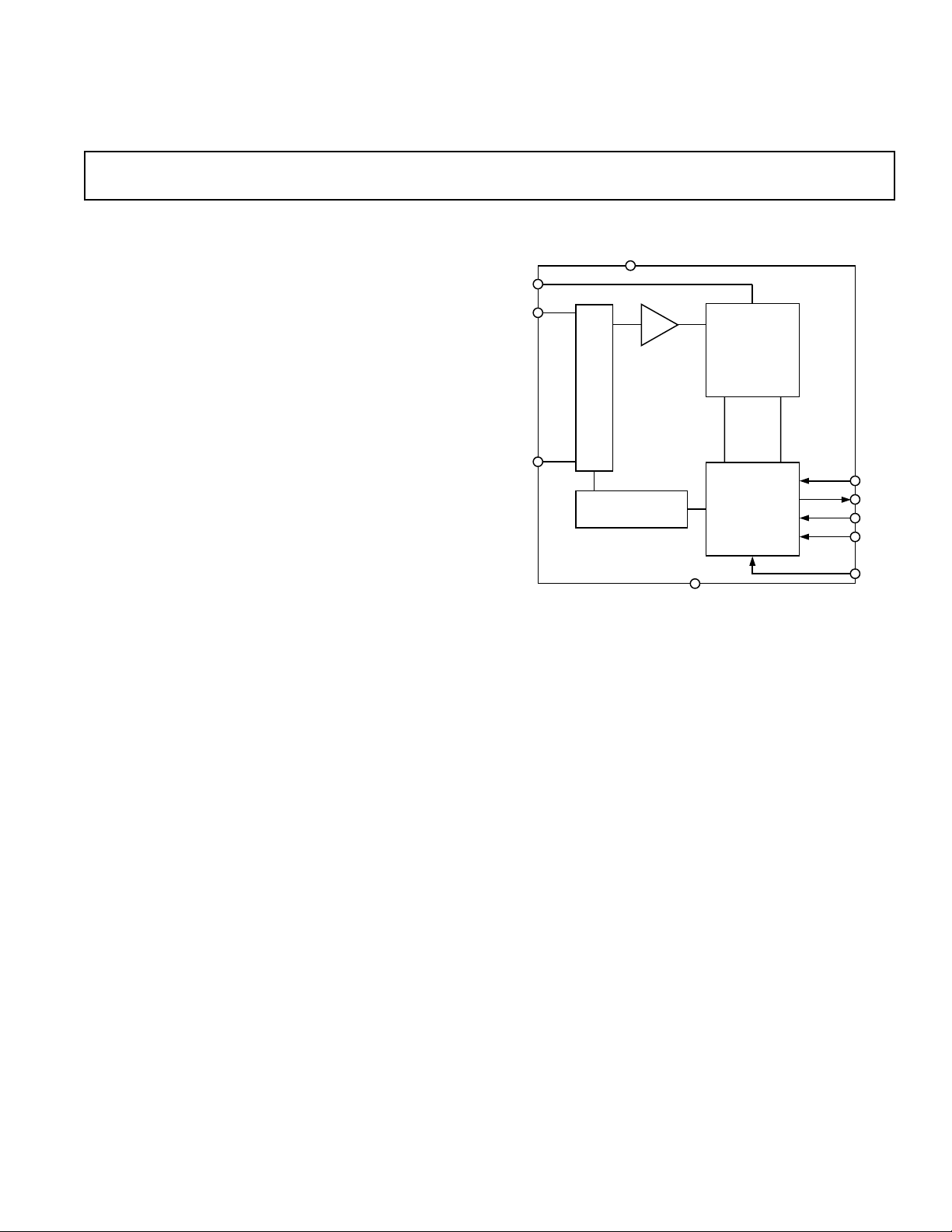
FUNCTIONAL BLOCK DIAGRAM
V
DD
REF
IN
VIN0
•
•
•
•
•
•
•
•
•
•
•
•
•
3
V
IN
I/P
MUX
AD7904/AD7914/AD7924
PRODUCT HIGHLIGHTS
1. High Throughput with Low Power Consumption.
The AD7904/AD7914/AD7924 offer up to 1 MSPS throughput rates. At the maximum throughput rate with 3 V sup`plies,
the AD7904/AD7914/AD7924 dissipate just 6 mW of
power maximum.
2. Four Single-Ended Inputs with a Channel Sequencer.
A consecutive sequence of channels can be selected, through
which the ADC will cycle and convert on.
3. Single-Supply Operation with V
The AD7904/AD7914/AD7924 operate from a single 2.7 V
to 5.25 V supply. The V
face to connect directly to either 3 V or 5 V processor systems
independent of V
4. Flexible Power/Serial Clock Speed Management.
The conversion rate is determined by the serial clock, allowing
the conversion time to be reduced through the serial clock speed
increase. The parts also feature various shutdown modes to
maximize power efficiency at lower throughput rates. Current
consumption is 0.5 µA max when in full shutdown.
5. No Pipeline Delay.
The parts feature a standard successive-approximation ADC
with accurate control of the sampling instant via a CS input
and once off conversion control.
T/H
SEQUENCER
.
DD
8-/10-/12-BIT
SUCCESSIVE
APPROXIMATION
ADC
CONTROL LOGIC
GND
Function.
DRIVE
function allows the serial inter-
DRIVE
SCLK
DOUT
DIN
CS
V
DRIVE
REV. 0
Information furnished by Analog Devices is believed to be accurate and
reliable. However, no responsibility is assumed by Analog Devices for its
use, nor for any infringements of patents or other rights of third parties that
may result from its use. No license is granted by implication or otherwise
under any patent or patent rights of Analog Devices.
One Technology Way, P.O. Box 9106, Norwood, MA 02062-9106, U.S.A.
Tel: 781/329-4700www.analog.com
Fax: 781/326-8703 © Analog Devices, Inc., 2002
AD7904–SPECIFICATIONS
(AVDD = V
= 2.7 V to 5.25 V, REFIN = 2.5 V, f
DRIVE
unless otherwise noted.)
= 20 MHz, TA = T
SCLK
MIN
to T
MAX
,
Parameter B Version
DYNAMIC PERFORMANCE f
Signal-to-Noise + Distortion (SINAD)
Signal-to-Noise Ratio (SNR)
2
Total Harmonic Distortion (THD)
Peak Harmonic or Spurious Noise
(SFDR)
2
Intermodulation Distortion (IMD)
2
2
2
49 dB min
49 dB min
–66 dB max
–64 dB max
1
Unit Test Conditions/Comments
= 50 kHz Sine Wave, f
IN
SCLK
= 20 MHz
fa = 40.1 kHz, fb = 41.5 kHz
Second Order Terms –90 dB typ
Third Order Terms –90 dB typ
Aperture Delay 10 ns typ
Aperture Jitter 50 ps typ
Channel-to-Channel Isolation
2
–85 dB typ fIN = 400 kHz
Full Power Bandwidth 8.2 MHz typ @ 3 dB
1.6 MHz typ @ 0.1 dB
DC ACCURACY
2
Resolution 8 Bits
Integral Nonlinearity ± 0.2 LSB max
Differential Nonlinearity ± 0.2 LSB max Guaranteed No Missed Codes to 8 Bits
0 V to REF
Input Range Straight Binary Output Coding
IN
Offset Error ± 0.5 LSB max
Offset Error Match ± 0.05 LSB max
Gain Error ± 0.2 LSB max
Gain Error Match ± 0.05 LSB max
0 V to 2 × REF
Input Range –REFIN to +REFIN Biased about REFIN with
IN
Positive Gain Error ± 0.2 LSB max Twos Complement Output Coding
Positive Gain Error Match ±0.05 LSB max
Zero Code Error ± 0.5 LSB max
Zero Code Error Match ± 0.1 LSB max
Negative Gain Error ± 0.2 LSB max
Negative Gain Error Match ± 0.05 LSB max
ANALOG INPUT
Input Voltage Range 0 to REF
0 to 2 × REF
IN
V RANGE Bit Set to 1
V RANGE Bit Set to 0, VDD/V
IN
= 4.75 V to 5.25 V
DRIVE
DC Leakage Current ± 1 µA max
Input Capacitance 20 pF typ
REFERENCE INPUT
REFIN Input Voltage 2.5 V ± 1% Specified Performance
DC Leakage Current ± 1 µA max
REFIN Input Impedance 36 kΩ typ f
SAMPLE
= 1 MSPS
LOGIC INPUTS
Input High Voltage, V
Input Low Voltage, V
Input Current, I
Input Capacitance, C
INL
IN
IN
INH
3
0.7 × V
0.3 × V
DRIVE
DRIVE
V min
V max
± 1 µA max Typically 10 nA, V
10 pF max
= 0 V or V
IN
DRIVE
LOGIC OUTPUTS
Output High Voltage, V
Output Low Voltage, V
Floating-State Leakage Current ± 1 µA max
Floating-State Output Capacitance
OH
OL
3
V
– 0.2 V min I
DRIVE
0.4 V max I
10 pF max
= 200 µA, VDD = 2.7 V to 5.25 V
SOURCE
= 200 µA
SINK
Output Coding Straight (Natural) Binary Coding Bit Set to 1
Twos Complement Coding Bit Set to 0
CONVERSION RATE
Conversion Time 800 ns max 16 SCLK Cycles with SCLK at 20 MHz
Track/Hold Acquisition Time 300 ns max Sine Wave Input
300 ns max Full-Scale Step Input
Throughput Rate 1 MSPS max See Serial Interface Section
–2– REV. 0

AD7904/AD7914/AD7924
Parameter B Version
POWER REQUIREMENTS
V
DD
V
DRIVE
2.7/5.25 V min/max
2.7/5.25 V min/max
I
1
Unit Test Conditions/Comments
–3–REV. 0
AD7914–SPECIFICATIONS
(AVDD = V
= 2.7 V to 5.25 V, REFIN = 2.5 V, f
DRIVE
unless otherwise noted.)
= 20 MHz, TA = T
SCLK
MIN
to T
MAX
,
Parameter B Version
DYNAMIC PERFORMANCE f
Signal-to-Noise + Distortion (SINAD)
Signal-to-Noise Ratio (SNR)
2
Total Harmonic Distortion (THD)
Peak Harmonic or Spurious Noise
(SFDR)
2
Intermodulation Distortion (IMD)
2
2
2
61 dB min
61 dB min
–72 dB max
–74 dB max
1
Unit Test Conditions/Comments
= 50 kHz Sine Wave, f
IN
fa = 40.1 kHz, fb = 41.5 kHz
SCLK
= 20 MHz
Second Order Terms –90 dB typ
Third Order Terms –90 dB typ
Aperture Delay 10 ns typ
Aperture Jitter 50 ps typ
Channel-to-Channel Isolation
2
–85 dB typ fIN = 400 kHz
Full Power Bandwidth 8.2 MHz typ @ 3 dB
1.6 MHz typ @ 0.1 dB
DC ACCURACY
2
Resolution 10 Bits
Integral Nonlinearity ± 0.5 LSB max
Differential Nonlinearity ± 0.5 LSB max Guaranteed No Missed Codes to 10 Bits
0 V to REF
Input Range Straight Binary Output Coding
IN
Offset Error ± 2LSB max
Offset Error Match ± 0.2 LSB max
Gain Error ± 0.5 LSB max
Gain Error Match ± 0.2 LSB max
0 V to 2 × REF
Input Range –REFIN to +REFIN Biased about REFIN with
IN
Positive Gain Error ± 0.5 LSB max Twos Complement Output Coding
Positive Gain Error Match ± 0.2 LSB max
Zero Code Error ±2LSB max
Zero Code Error Match ±0.2 LSB max
Negative Gain Error ± 0.5 LSB max
Negative Gain Error Match ± 0.2 LSB max
ANALOG INPUT
Input Voltage Range 0 to REF
0 to 2 × REF
IN
V RANGE Bit Set to 1
V RANGE Bit Set to 0, VDD/V
IN
= 4.75 V to 5.25 V
DRIVE
DC Leakage Current ± 1 µA max
Input Capacitance 20 pF typ
REFERENCE INPUT
REFIN Input Voltage 2.5 V ± 1% Specified Performance
DC Leakage Current ± 1 µA max
REFIN Input Impedance 36 kΩ typ f
SAMPLE
= 1 MSPS
LOGIC INPUTS
Input High Voltage, V
Input Low Voltage, V
Input Current, I
Input Capacitance, C
INL
IN
IN
INH
3
0.7 × V
0.3 × V
DRIVE
DRIVE
V min
V max
± 1 µA max Typically 10 nA, V
10 pF max
= 0 V or V
IN
DRIVE
LOGIC OUTPUTS
Output High Voltage, V
Output Low Voltage, V
Floating-State Leakage Current ± 1 µA max
Floating-State Output Capacitance
OH
OL
3
V
– 0.2 V min I
DRIVE
0.4 V max I
10 pF max
= 200 µA, VDD = 2.7 V to 5.25 V
SOURCE
= 200 µA
SINK
Output Coding Straight (Natural) Binary Coding Bit Set to 1
Twos Complement Coding Bit Set to 0
CONVERSION RATE
Conversion Time 800 ns max 16 SCLK Cycles with SCLK at 20 MHz
Track/Hold Acquisition Time 300 ns max Sine Wave Input
300 ns max Full-Scale Step Input
Throughput Rate 1 MSPS max See Serial Interface Section
–4– REV. 0
AD7904/AD7914/AD7924
Parameter B Version
1
Unit Test Conditions/Comments
POWER REQUIREMENTS
V
DD
V
DRIVE
I
DD
4
2.7/5.25 V min/max
2.7/5.25 V min/max
Digital I/Ps = 0 V or V
DRIVE
Normal Mode (Static) 600 µA typ VDD = 2.7 V to 5.25 V, SCLK On or Off
Normal Mode (Operational) 2.7 mA max V
2 mA max V
Using Auto Shutdown Mode 960 µA typ f
= 4.75 V to 5.25 V, f
DD
= 2.7 V to 3.6 V, f
DD
= 250 kSPS
SAMPLE
SCLK
= 20 MHz
SCLK
= 20 MHz
0.5 µA max (Static)
Full Shutdown Mode 0.5 µA max SCLK On or Off (20 nA typ)
Power Dissipation
Normal Mode (Operational) 13.5 mW max VDD = 5 V, f
Auto Shutdown Mode (Static) 2.5 µW max V
Full Shutdown Mode 2.5 µW max V
4
= 20 MHz
6 mW max V
1.5 µW max V
= 3 V, f
DD
= 5 V
DD
= 3 V
DD
= 5 V
DD
SCLK
= 20 MHz
SCLK
1.5 µW max VDD = 3 V
NOTES
1
Temperature ranges as follows: B Version: –40°C to +85°C.
2
See Terminology section.
3
Sample tested @ 25°C to ensure compliance.
4
See Power Versus Throughput Rate section.
Specifications subject to change without notice.
–5–REV. 0
AD7924–SPECIFICATIONS
(AVDD = V
= 2.7 V to 5.25 V, REFIN = 2.5 V, f
DRIVE
unless otherwise noted.)
= 20 MHz, TA = T
SCLK
MIN
to T
MAX
,
Parameter B Version
DYNAMIC PERFORMANCE f
Signal to Noise + Distortion (SINAD)
Signal to Noise Ratio (SNR)
2
Total Harmonic Distortion (THD)
2
70 dB min @ 5 V
69 dB min @ 3 V Typically 69.5 dB
2
70 dB min
–77 dB max @ 5 V Typically –84 dB
1
Unit Test Conditions/Comments
= 50 kHz Sine Wave, f
IN
SCLK
= 20 MHz
–73 dB max @ 3 V Typically –77 dB
Peak Harmonic or Spurious Noise –78 dB max @ 5 V Typically –86 dB
(SFDR)
Intermodulation Distortion (IMD)
2
2
–76 dB max @ 3 V Typically –80 dB
fa = 40.1 kHz, fb = 41.5 kHz
Second Order Terms –90 dB typ
Third Order Terms –90 dB typ
Aperture Delay 10 ns typ
Aperture Jitter 50 ps typ
Channel-to-Channel Isolation
2
–85 dB typ fIN = 400 kHz
Full Power Bandwidth 8.2 MHz typ @ 3 dB
1.6 MHz typ @ 0.1 dB
DC ACCURACY
2
Resolution 12 Bits
Integral Nonlinearity ± 1 LSB max
Differential Nonlinearity –0.9/+1.5 LSB max Guaranteed No Missed Codes to 12 Bits
0 V to REF
Input Range Straight Binary Output Coding
IN
Offset Error ± 8 LSB max Typically ±0.5 LSB
Offset Error Match ± 0.5 LSB max
Gain Error ± 1.5 LSB max
Gain Error Match ± 0.5 LSB max
0 V to 2 × REF
Input Range –REFIN to +REFIN Biased about REFIN with
IN
Positive Gain Error ± 1.5 LSB max Twos Complement Output Coding
Positive Gain Error Match ± 0.5 LSB max
Zero Code Error ±8 LSB max Typically ± 0.8 LSB
Zero Code Error Match ±0.5 LSB max
Negative Gain Error ± 1 LSB max
Negative Gain Error Match ±0.5 LSB max
ANALOG INPUT
Input Voltage Range 0 to REF
0 to 2 × REF
V RANGE Bit Set to 1
IN
V RANGE Bit Set to 0, VDD/V
IN
= 4.75 V to 5.25 V
DRIVE
DC Leakage Current ± 1 µA max
Input Capacitance 20 pF typ
REFERENCE INPUT
REFIN Input Voltage 2.5 V ±1% Specified Performance
DC Leakage Current ± 1 µA max
REFIN Input Impedance 36 kΩ typ f
SAMPLE
= 1 MSPS
LOGIC INPUTS
Input High Voltage, V
Input Low Voltage, V
Input Current, I
Input Capacitance, C
INL
IN
IN
INH
3
0.7 × V
0.3 × V
DRIVE
DRIVE
V min
V max
± 1 µA max Typically 10 nA, V
10 pF max
= 0 V or V
IN
DRIVE
LOGIC OUTPUTS
Output High Voltage, V
Output Low Voltage, V
Floating-State Leakage Current ± 1 µA max
Floating-State Output Capacitance
OH
OL
3
V
– 0.2 V min I
DRIVE
0.4 V max I
10 pF max
= 200 µA, VDD = 2.7 V to 5.25 V
SOURCE
= 200 µA
SINK
Output Coding Straight (Natural) Binary Coding Bit Set to 1
Twos Complement Coding Bit Set to 0
–6– REV. 0
AD7904/AD7914/AD7924
Parameter B Version
1
Unit Test Conditions/Comments
CONVERSION RATE
Conversion Time 800 ns max 16 SCLK Cycles with SCLK at 20 MHz
Track/Hold Acquisition Time 300 ns max Sine Wave Input
300 ns max Full-Scale Step Input
Throughput Rate 1 MSPS max See Serial Interface Section
POWER REQUIREMENTS
V
DD
V
DRIVE
I
DD
4
2.7/5.25 V min/max
2.7/5.25 V min/max
Digital I/Ps = 0 V or V
DRIVE
Normal Mode(Static) 600 µA typ VDD = 2.7 V to 5.25 V, SCLK On or Off
Normal Mode (Operational) 2.7 mA max V
2 mA max V
Using Auto Shutdown Mode 960 µA typ f
= 4.75 V to 5.25 V, f
DD
= 2.7 V to 3.6 V, f
DD
= 250 kSPS
SAMPLE
SCLK
= 20 MHz
SCLK
= 20 MHz
0.5 µA max (Static)
Full Shutdown Mode 0.5 µA max SCLK On or Off (20 nA typ)
Power Dissipation
Normal Mode (Operational) 13.5 mW max VDD = 5 V, f
Auto Shutdown Mode (Static) 2.5 µW max V
Full Shutdown Mode 2.5 µW max V
4
= 20 MHz
6 mW max V
1.5 µW max V
= 3 V, f
DD
= 5 V
DD
= 3 V
DD
= 5 V
DD
SCLK
= 20 MHz
SCLK
1.5 µW max VDD = 3 V
NOTES
1
Temperature ranges as follows: B Versions: –40°C to +85°C.
2
See Terminology section.
3
Sample tested @ 25°C to ensure compliance.
4
See Power Versus Throughput Rate section.
Specifications subject to change without notice.
–7–REV. 0
AD7904/AD7914/AD7924
TIMING SPECIFICATIONS
Limit at T
MIN
1
(VDD = 2.7 V to 5.25 V, V
, T
AD7904/AD7914/AD7924
MAX
ⱕ VDD, REFIN = 2.5 V, TA = T
DRIVE
MIN
to T
, unless otherwise noted.)
MAX
Parameter VDD = 3 V VDD = 5 V Unit Description
f
SCLK
2
10 10 kHz min
20 20 MHz max
t
CONVERT
t
QUIET
16 × t
SCLK
16 × t
SCLK
50 50 ns min Minimum Quiet Time Required Between CS Rising Edge
and Start of Next Conversion
t
2
3
t
3
3
t
4
t
5
t
6
t
7
4
t
8
t
9
t
10
t
11
t
12
10 10 ns min CS to SCLK Setup Time
35 30 ns max Delay from CS until DOUT Three-State Disabled
40 40 ns max Data Access Time after SCLK Falling Edge
0.4 × t
0.4 × t
SCLK
SCLK
0.4 × t
0.4 × t
SCLK
SCLK
ns min SCLK Low Pulsewidth
ns min SCLK High Pulsewidth
10 10 ns min SCLK to DOUT Valid Hold Time
15/45 15/35 ns min/max SCLK Falling Edge to DOUT High Impedance
10 10 ns min DIN Setup Time Prior to SCLK Falling Edge
55 ns min DIN Hold Time after SCLK Falling Edge
20 20 ns min Sixteenth SCLK Falling Edge to CS High
11 µs max Power-Up Time from Full Power-Down/Auto
Shutdown Modes
NOTES
1
Sample tested at 25°C to ensure compliance. All input signals are specified with tr = tf = 5 ns (10% to 90% of VDD) and timed from a voltage level of 1.6 V.
See Figure 1. The 3 V operating range spans from 2.7 V to 3.6 V. The 5 V operating range spans from 4.75 V to 5.25 V.
2
Mark/Space ratio for the SCLK input is 40/60 to 60/40.
3
Measured with the load circuit of Figure 1 and defined as the time required for the output to cross 0.4 V or 0.7 × V
4
t8 is derived form the measured time taken by the data outputs to change 0.5 V when loaded with the circuit of Figure 1. The measured number is then extrapolated
back to remove the effects of charging or discharging the 50 pF capacitor. This means that the time, t
time of the part and is independent of the bus loading.
Specifications subject to change without notice.
, quoted in the timing characteristics is the true bus relinquish
8
DRIVE
.
–8–
REV. 0
 Loading...