5 V Single Supply
a
FEATURES
Fast (2.2 s) 14-Bit ADC
400 kSPS Throughput Rate
0.3 s Track/Hold Acquisition Time
Single Supply Operation
Selection of Input Ranges: ⴞ10 V, ⴞ5 V and ⴞ2.5 V
0 V to 2.5 V and 0 V to 5 V
High-Speed Parallel Interface which Also Allows
Interfacing to 3 V Processors
Low Power, 80 mW Typ
Power-Saving Mode, 20 W Typ
Overvoltage Protection on Analog Inputs
Power-Down Mode via STBY Pin
GENERAL DESCRIPTION
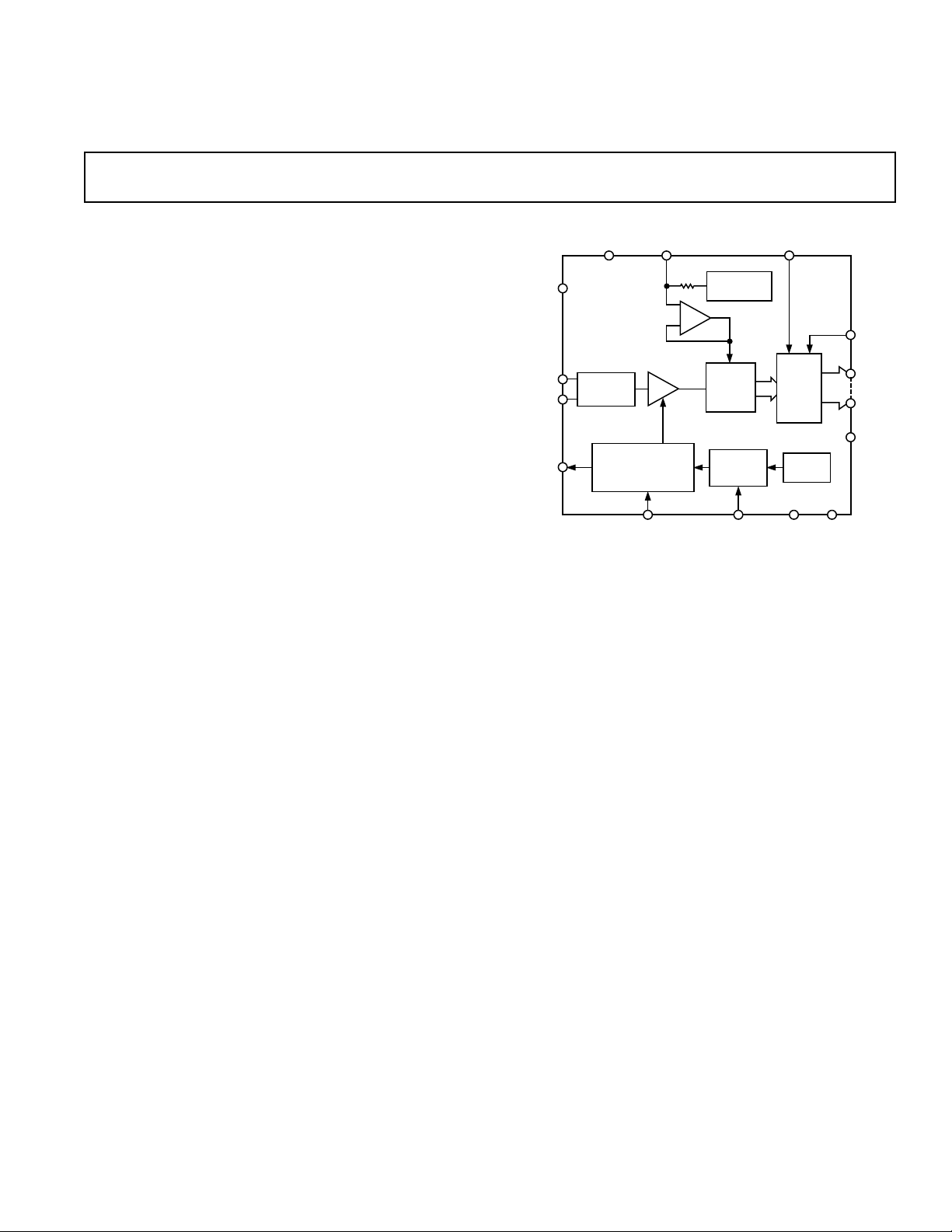
The AD7899 is a fast, low-power, 14-bit A/D converter that
operates from a single 5 V supply. The part contains a 2.2 µs
successive-approximation ADC, a track/hold amplifier, 2.5 V
reference, on-chip clock oscillator, signal conditioning circuitry,
and a high-speed parallel interface. The part accepts analog input
ranges of ±10 V, ± 5 V, ± 2.5 V, 0 V to 2.5 V, and 0 V to 5 V.
Overvoltage protection on the analog input for the part allows
the input voltage to be exceeded without damaging the parts.
Speed of conversion can be controlled either by an internally
trimmed clock oscillator or by an external clock.
A conversion start signal (CONVST) places the track/hold into
hold mode and initiates conversion. The BUSY/EOC signal
indicates the end of the conversion.
Data is read from the part via a 14-bit parallel data bus using the
standard CS and RD signals. Maximum throughput for the
AD7899 is 400 kSPS.
The AD7899 is available in a 28-lead SOIC and SSOP packages.
14-Bit 400 kSPS ADC
AD7899
FUNCTIONAL BLOCK DIAGRAM
V
REF
6k⍀
REFERENCE
+
–
14-BIT
ADC
CONVERSION
CONTROL
LOGIC
CONVST OPGNDGND
INT/EXT
CLOCK
SELECT
CLKIN
STBY
V
INA
V
INB
BUSY/EOC
AVDD
AD7899
TRACK/HOLD
SIGNAL
SCALING
PRODUCT HIGHLIGHTS
1. The AD7899 features a fast (2.2 µs) ADC allowing throughput rates of up to 400 kSPS.
2. The AD7899 operates from a single 5 V supply and consumes only 80 mW typ making it ideal for low power and
portable applications.
3. The part offers a high-speed parallel interface. The interface
can operate in 3 V and 5 V mode allowing for easy connection to 3 V or 5 V microprocessors, microcontrollers, and
digital signal processors.
4. The part is offered in three versions with different analog
input ranges. The AD7899-1 offers the standard industrial
ranges of ±10 V and ± 5 V; the AD7899-2 offers a unipolar
range of 0 V to 2.5 or 0 V to 5 V, and the AD7899-3 has an
input range of ±2.5 V.
2.5V
V
DRIVE
OUTPUT
LATCH
CLOCK
RD
DB13
DB0
CS
INT
REV. A
Information furnished by Analog Devices is believed to be accurate and
reliable. However, no responsibility is assumed by Analog Devices for its
use, nor for any infringements of patents or other rights of third parties that
may result from its use. No license is granted by implication or otherwise
under any patent or patent rights of Analog Devices.
One Technology Way, P.O. Box 9106, Norwood, MA 02062-9106, U.S.A.
Tel: 781/329-4700 www.analog.com
Fax: 781/326-8703 © Analog Devices, Inc., 2001

AD7899–SPECIFICATIONS
(VDD = 5 V ⴞ 5%, AGND = DGND = 0 V, V
T
to T
MIN
and valid for V
MAX
= 3 V ⴞ 5% and 5 V ⴞ 5% unless otherwise noted.)
DRIVE
= Internal. Clock = Internal, all specifications
REF
ABS
Parameter Version
1
Version
1
Version
1
Unit Test Conditions/Comments
SAMPLE AND HOLD
–0.1 dB Full Power Bandwidth 500 500 500 kHz typ
–3 dB Full Power Bandwidth 4.5 4.5 4.5 MHz typ
Aperture Delay 20 20 20 ns max
Aperture Jitter 25 25 25 ps typ
DYNAMIC PERFORMANCE
2
fIN = 100 kHz, fS = 400 kSPS
AD7899-1
Signal to (Noise + Distortion)
3
@ 25C 78 78 78 dB min
Ratio
to T
T
MIN
Total Harmonic Distortion
MAX
3
Peak Harmonic or Spurious Noise
78 78 77 dB min
–84 –84 –82 dB max
3
–86 –86 –85 dB max
AD7899-2
Signal to (Noise + Distortion)
3
@ 25C 78 dB min
Ratio
to T
T
MIN
Total Harmonic Distortion
MAX
3
Peak Harmonic or Spurious Noise
77 dB min
–82 dB max
3
–82 dB max
AD7899-3
Signal to (Noise + Distortion)
3
@ 25C 78 78 dB min
Ratio
to T
T
MIN
Total Harmonic Distortion
Peak Harmonic or Spurious Noise
Intermodulation Distortion
MAX
3
3
77 77 dB min
–84 –84 dB max
3
–86 –86 dB max
fa = 49 kHz, fb = 50 kHz
2nd Order Terms –89 –89 –89 dB typ
3rd Order Terms –89 –89 –89 dB typ
DC ACCURACY
Resolution 14 14 14 Bits
Relative Accuracy (INL)
Differential Nonlinearity (DNL)
3
± 2 ± 1.5 ±2 LSB max
3
± 1 ± 1 ± 1 LSB max No Missing Codes Guaranteed
AD7899-1
Input Voltage Range ± 5, ± 10 ± 5, ± 10 Volts
Input Current 0.8, 0.8 0.8, 0.8 mA max V
Positive Gain Error
Negative Gain Error
3
3
± 10 ± 8 ± 12 LSB max
± 10 ± 8 ± 12 LSB max
= –5 V and –10 V Respectively
IN
Bipolar Zero Error ± 12 ± 8 ± 12 LSB max
AD7899-2
Input Voltage Range 0 to 2.5 Volts
0 to 5
Input Current 0.4, 800 µA max V
Positive Gain Error
Offset Error
3
3
± 14 LSB max
± 10 LSB max
= 2.5 V, VIN = 5 V
IN
AD7899-3
Input Voltage Range ± 2.5 ± 2.5 Volts
Input Current 0.8 0.8 mA max V
Positive Gain Error
Negative Gain Error
3
3
± 14 ± 12 LSB max
± 14 ± 12 LSB max
= –2.5 V
IN
Bipolar Zero Error ± 14 ± 12 LSB max
REFERENCE INPUT/OUTPUT
V
IN Input Voltage Range 2.375/2.625 2.375/2.625 2.375/2.625 V
REF
IN Input Capacitance
V
REF
V
OUT Output Voltage 2.5 2.5 2.5 V nom
REF
OUT Error @ 25C ± 10 ± 10 ± 10 mV max
V
REF
OUT Error T
V
REF
V
OUT Temperature Coefficient 25 25 25 ppm/C typ
REF
V
OUT Output Impedance 6 6 6 kΩ typ See Reference Section
REF
MIN
to T
4
MAX
10 10 10 pF max
± 20 ± 20 ± 25 mV max
MIN/VMAX
2.5 V ± 5%
–2–
REV. A

AD7899
ABS
Parameter Version
L
OGIC INPUTS
Input High Voltage, V
Input Low Voltage, V
Input Current, I
IN
Input Capacitance, C
INH
INL
IN
4
V
V
± 10 ± 10 ± 10 µA max
10 10 10 pF max
DRIVE
DRIVE
1
/2 + 0.4 V
/2 – 0.4 V
Version
/2 + 0.4 V
DRIVE
/2 – 0.4 V
DRIVE
1
Version
1
/2 + 0.4 V min VDD = 5 V ± 5%
DRIVE
/2 – 0.4 V max VDD = 5 V ± 5%
DRIVE
Unit Test Conditions/Comments
LOGIC OUTPUTS
Output High Voltage, V
Output Low Voltage, V
OL
OH
– 0.4 V
DRIVE
0.4 0.4 0.4 V max I
DRIVE
– 0.4 V
– 0.4 V min I
DRIVE
SOURCE
= 1.6 mA
SINK
= 400 µA
V
DB13–DB0
High Impedance
Leakage Current ± 10 ± 10 ± 10 µA max
Capacitance
4
10 10 10 pF max
Output Coding
AD7899-1, AD7899-3 Two’s Complement
AD7899-2 Straight (Natural) Binary
CONVERSION RATE
Conversion Time 2.2 2.2 2.2 µs max
Track/Hold Acquisition Time
2, 3
0.3 0.3 0.3 µs max
Throughput Time 400 400 400 kSPS max
POWER REQUIREMENTS
V
DD
I
DD
5 5 5 V nom
Normal Mode 25 25 25 mA max Typically 16 mA
Standby Mode 20 20 20 µA max (5 µA typ) Logic Inputs = 0 V or
V
DD
Power Dissipation
Normal Mode 125 125 125 mW max Typically 80 mW, V
DD
Standby Mode 100 100 125 µW max
NOTES
1
Temperature Ranges are as follows : A, B Versions: –40C to +85C. S Version: –55°C to +125°C.
2
Performance measured through full channel (SHA and ADC).
3
See Terminology.
4
Sample tested @ 25°C to ensure compliance.
Specifications subject to change without notice.
= 5 V
REV. A
–3–
AD7899
1, 2
TIMING CHARACTERISTICS
to T
and valid for V
MAX
= 3 V ⴞ 5% and 5 V ⴞ 5% unless otherwise noted.)
DRIVE
(VDD = 5 V ⴞ 5%, AGND = DGND = 0 V, V
A, B and S
Parameter Versions Unit Test Conditions/Comments
t
CONV
2.2 µs max Conversion Time, Internal Clock
2.46 µs max CLKIN = 6.5 MHz
t
ACQ
t
EOC
t
WAKE-UP
– External V
REF
5
0.3 µs max Acquisition Time
120 ns min EOC Pulsewidth
180 ns max
2 µs max STBY Rising Edge to CONVST Rising Edge
(See Standby Mode Operation)
t
1
t
2
35 ns min CONVST Pulsewidth
70 ns min CONVST Rising Edge to BUSY Rising Edge
Read Operation
t
3
t
4
t
5
3
t
6
4
t
7
0 ns min CS to RD Setup Time
0 ns min CS to RD Hold Time
35 ns min Read Pulsewidth
35 ns max Data Access Time after Falling Edge of RD, V
40 ns max Data Access Time after Falling Edge of RD, V
5 ns min Bus Relinquish Time after Rising Edge of RD
30 ns max
t
8
0 ns min BUSY Falling Edge to RD Delay
External Clock
t
9
t
10
t
11
NOTES
1
Sample tested at 25°C to ensure compliance. All input signals are measured with tr = tf = 1 ns (10% to 90% of V
2
See Figures 5, 6, 7, and 8.
3
Measured with the load circuit of Figure 1 and defined as the time required for an output to cross 0.8 V or 2.0 V.
4
These times are derived from the measured time taken by the data outputs to change 0.5 V when loaded with the circuit of Figure 1. The measured number is then
extrapolated back to remove the effects of charging or discharging the 50 pF capacitor. This means that the times quoted in the timing characteristics are the true bus
relinquish times of the part and as such are independent of external bus loading capacitances.
5
Refer to the Standby Mode Operation section.
Specifications subject to change without notice.
0 ns min CLKIN to CONVST Rising Edge Setup Time
20 ns min CLKIN to CONVST Rising Edge Hold Time
100 ns min CONVST Rising Edge to CLK Falling Edge
= Internal, Clock = Internal; All specifications T
REF
DRIVE
DRIVE
) and timed from a voltage level of V
DRIVE
= 5 V
= 3 V
/2.
DRIVE
MIN
1.6mA
OUTPUT
PIN
TO
50pF
400A
1.6V
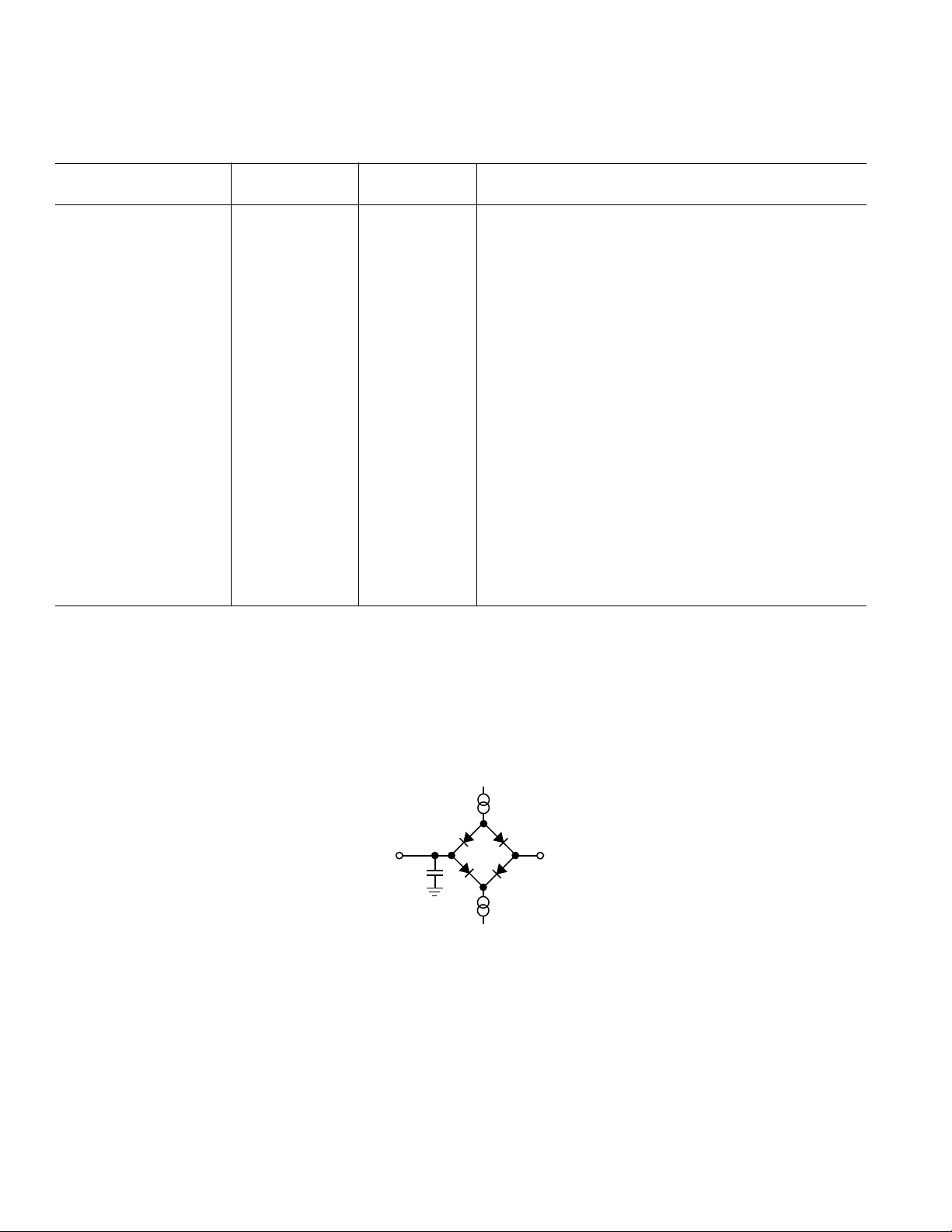
Figure 1. Load Circuit for Access Time and Bus Relinquish Time
–4–
REV. A
AD7899
WARNING!
ESD SENSITIVE DEVICE
ABSOLUTE MAXIMUM RATINGS*
(TA = 25°C unless otherwise noted)
VDD to AGND . . . . . . . . . . . . . . . . . . . . . . . . . –0.3 V to +7 V
V
to DGND . . . . . . . . . . . . . . . . . . . . . . . . . –0.3 V to +7 V
DD
V
to DGND . . . . . . . . . . . . . . . . . . . . . . . . . V
DRIVE
+ 0.3 V
DD
Analog Input Voltage to AGND
AD7899-1 (±10 V Range) . . . . . . . . . . . . . . . . . . . . ± 18 V
AD7899-1 (±5 V Range) . . . . . . . . . . . . . . . –9 V to +18 V
AD7899-2 . . . . . . . . . . . . . . . . . . . . . . . . . . –1 V to +18 V
AD7899-3 . . . . . . . . . . . . . . . . . . . . . . . . . . –4 V to +18 V
Reference Input Voltage to AGND . . . –0.3 V to V
Digital Input Voltage to DGND . . . . . –0.3 V to V
Digital Output Voltage to DGND . . . . –0.3 V to V
+ 0.3 V
DD
+ 0.3 V
DD
+ 0.3 V
DD
Operating Temperature Range
Commercial (A, B Version) . . . . . . . . . . . –40°C to +85°C
SOIC Package, Power Dissipation . . . . . . . . . . . . . . . 450 mW
Thermal Impedance . . . . . . . . . . . . . . . . . . . . . . . 95°C/W
θ
JA
Lead Temperature, Soldering
Vapor Phase (60 sec) . . . . . . . . . . . . . . . . . . . . 215°C
Infrared (15 sec) . . . . . . . . . . . . . . . . . . . . . . . . 220°C
SSOP Package, Power Dissipation . . . . . . . . . . . . . . . 450 mW
Thermal Impedance . . . . . . . . . . . . . . . . . . . . . . . 95°C/W
θ
JA
Lead Temperature, Soldering
Vapor Phase (60 sec) . . . . . . . . . . . . . . . . . . . . . 215°C
Infrared (15 sec) . . . . . . . . . . . . . . . . . . . . . . . . . 220°C
*
Stresses above those listed under Absolute Maximum Ratings may cause permanent damage to the device. This is a stress rating only; functional operation of the
device at these or any other conditions above those listed in the operational
sections of this specification is not implied. Exposure to absolute maximum rating
conditions for extended periods may affect device reliability.
Military (S Version) . . . . . . . . . . . . . . . . . –55°C to +125°C
Storage Temperature Range . . . . . . . . . . . –65°C to +150°C
Junction Temperature . . . . . . . . . . . . . . . . . . . . . . . 150°C
CAUTION
ESD (electrostatic discharge) sensitive device. Electrostatic charges as high as 4000 V readily
accumulate on the human body and test equipment and can discharge without detection. Although
the AD7899 features proprietary ESD protection circuitry, permanent damage may occur on
devices subjected to high-energy electrostatic discharges. Therefore, proper ESD precautions are
recommended to avoid performance degradation or loss of functionality.
ORDERING GUIDE
Relative Temperature Package Package
Model Input Ranges Accuracy Range Description Option
±
AD7899AR-1
AD7899BR-1
AD7899SR-1
5V, ±10 V
±
5V, ±10 V
±
5V, ±10 V
AD7899AR-2 0 V to 5 V, 0 V to 2.5 V
AD7899AR-3
AD7899BR-3
AD7899ARS-1
±
2.5 V
±
2.5 V
±
5V, ±10 V
AD7899ARS-2 0 V to 5 V, 0 V to 2.5 V
AD7899ARS-3
±
2.5 V
±
2 LSB –40C to +85C Small Outline R-28
±
1.5 LSB –40C to +85C Small Outline R-28
±
2 LSB –55C to +125C Small Outline R-28
±
2 LSB –40C to +85C Small Outline R-28
±
2 LSB –40C to +85C Small Outline R-28
±
1.5 LSB –40C to +85C Small Outline R-28
±
2 LSB –40C to +85C Shrink Small Outline RS-28
±
2 LSB –40C to +85C Shrink Small Outline RS-28
±
2 LSB –40C to +85C Shrink Small Outline RS-28
REV. A
–5–
 Loading...