Analog Devices AD7896 c Datasheet

2.7 V to 5.5 V, 12-Bit, 8 s
C
ADC in 8-Lead SOIC/PDIP
FEATURES
100 kHz Throughput Rate
Fast 12-Bit Sampling ADC with 8 s Conversion Time
8-Lead PDIP and SOIC
Single 2.7 V to 5.5 V Supply Operation
High Speed, Easy-to-Use Serial Interface
On-Chip Track-and-Hold Amplifier
Analog Input Range Is 0 V to Supply
High Input Impedance
Low Power: 9 mW Typ
GENERAL DESCRIPTION
The AD7896 is a fast, 12-bit ADC that operates from a single
2.7 V to 5.5 V supply and is housed in small 8-lead PDIP and
8-lead SOIC packages. The part contains an 8 µs successive
approximation ADC, an on-chip track-and-hold amplifier, an
on-chip clock, and a high speed serial interface.
Output data from the AD7896 is provided via a high speed,
serial interface port. This 2-wire serial interface has a serial
clock input and a serial data output with the external serial
clock accessing the serial data from the part.
In addition to the traditional dc accuracy specifications, such as
linearity, full-scale, and offset errors, the AD7896 is also specified for dynamic performance parameters, including harmonic
distortion and signal-to-noise ratio.
The part accepts an analog input range of 0 V to V
and operates
DD
from a single 2.7 V to 5.5 V supply, consuming only 9 mW
typical. The V
input is also used as the reference for the part
DD
so that no external reference is required.
The AD7896 features a high sampling rate mode and, for low
power applications, a proprietary automatic power-down mode
where the part automatically goes into power-down once conversion is complete and “wakes up” before the next conversion cycle.
The part is available in a small, 8-lead, 0.3'' wide, plastic or
hermetic dual-in-line package (PDIP) and in an 8-lead, small
outline IC (SOIC).
*
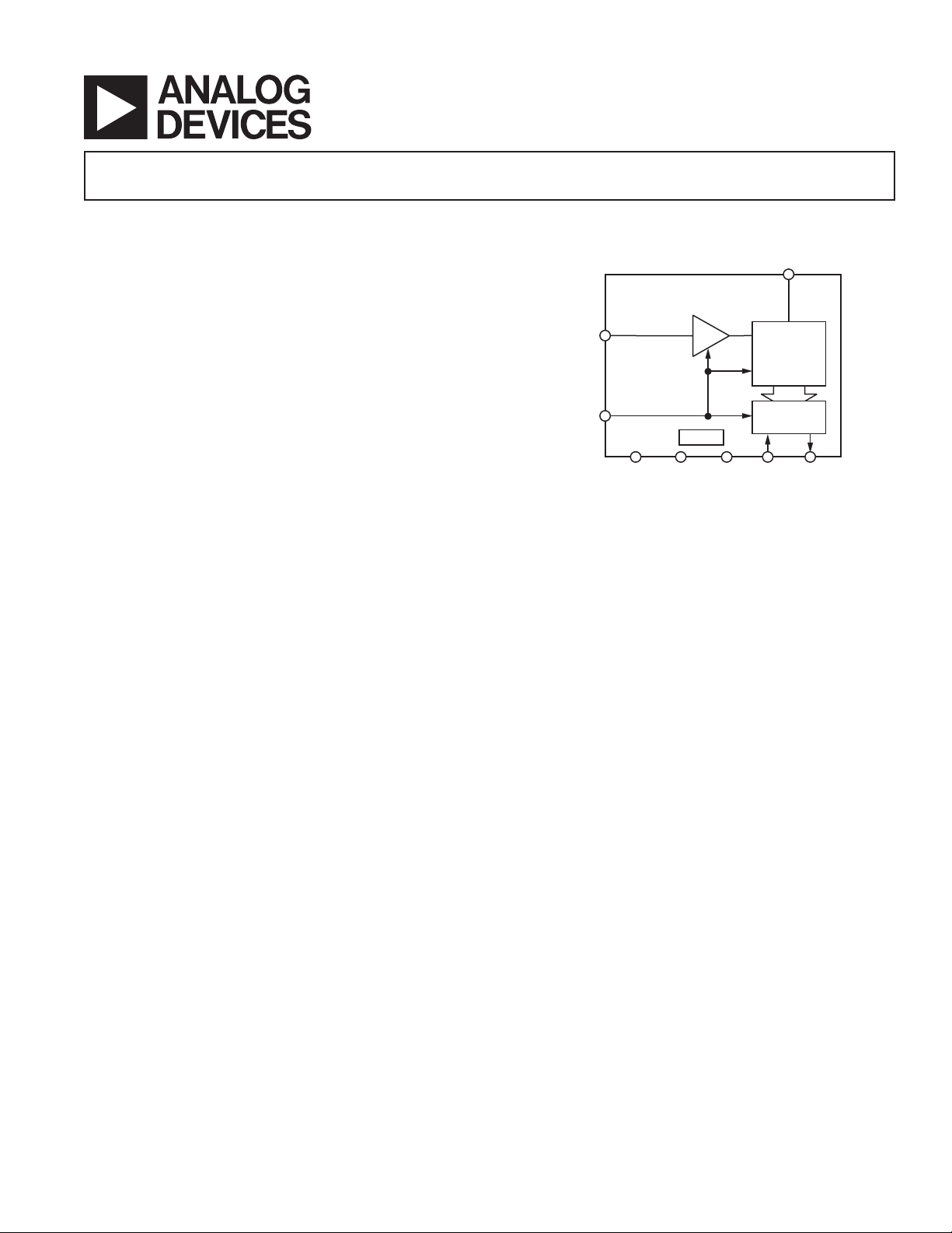
FUNCTIONAL BLOCK DIAGRAM
AD7896
TRACK-AND-HOLD
V
IN
ONVST
AGND DGND BUSY SCLK SDATA
PRODUCT HIGHLIGHTS
CLOCK
AD7896
V
DD
12-BIT
ADC
OUTPUT
REGISTER
1. Complete, 12-bit ADC in an 8-Lead Package.
The AD7896 contains an 8 µs ADC, a track-and-hold ampli-
fier, control logic, and a high speed serial interface, all in an
8-lead PDIP. The V
input is used as the reference for the
DD
part, so no external reference is needed. This offers considerable space saving over alternative solutions.
2. Low Power, Single-Supply Operation.
The AD7896 operates from a single 2.7 V to 5.5 V supply
and consumes only 9 mW typical. The automatic powerdown mode, where the part goes into power down once
conversion is complete and “wakes up” before the next conversion cycle, makes the AD7896 ideal for battery-powered
or portable applications.
3. High Speed Serial Interface.
The part provides high speed serial data and serial clock lines
allowing for an easy, 2-wire serial interface arrangement.
*Patent Pending
REV. C
Information furnished by Analog Devices is believed to be accurate and
reliable. However, no responsibility is assumed by Analog Devices for its
use, nor for any infringements of patents or other rights of third parties that
may result from its use. No license is granted by implication or otherwise
under any patent or patent rights of Analog Devices. Trademarks and
registered trademarks are the property of their respective companies.
One Technology Way, P.O. Box 9106, Norwood, MA 02062-9106, U.S.A.
Tel: 781/329-4700 www.analog.com
Fax: 781/326-8703 © 2003 Analog Devices, Inc. All rights reserved.

AD7896–SPECIFICATIONS
(VDD = 2.7 V to 5.5 V, AGND = DGND = 0 V. All specifications T
unless otherwise noted.)
MIN
to T
MAX
,
Test Conditions/
Parameter A Version1B Version J Version S Version Unit Comments
DYNAMIC PERFORMANCE
Signal-to-(Noise + Distortion) Ratio
2
3
@ 25°C707070 typ 70 dB min fIN = 10 kHz Sine Wave,
= 100 kHz
f
to T
T
MIN
MAX
70 dB min
SAMPLE
Total Harmonic Distortion (THD)3–80 –80 –80 typ –80 dB max fIN = 10 kHz Sine Wave,
= 100 kHz
f
Peak Harmonic or Spurious Noise
Intermodulation Distortion (IMD)
3
3
–80 –80 –80 typ dB max fIN = 10 kHz Sine Wave,
SAMPLE
f
= 100 kHz
SAMPLE
fa = 9 kHz, fb = 9.5 kHz,
= 100 kHz
f
SAMPLE
Second Order Terms –80 –80 –80 typ –80 dB max
Third Order Terms –80 –80 –80 typ –80 dB max
DC ACCURACY
Resolution 12 12 12 12 Bits
Minimum Resolution for Which No
Missing Codes Are Guaranteed 12 12 12 12 Bits
Relative Accuracy
Differential Nonlinearity
Positive Full-Scale Error
Unipolar Offset Error ± 4 ± 4 ± 5 ± 4LSB maxV
3
3
3
± 1 ± 1/2 ± 1 ± 1LSB max
± 1 ± 1 ± 1 ± 1LSB max
± 3 ± 1.5 ±3 ±3LSB max
= 5 V ± 10%
± 4 ± 3 ± 5 ± 4LSB maxV
DD
= 2.7 V to 3.6 V
DD
ANALOG INPUT
Input Voltage Range 0 to +V
DD
0to+V
0to+VDD0 to +VDDV
DD
Input Current ± 2 ± 2 ± 2 ± 5 µA max
LOGIC INPUTS
Input High Voltage, V
Input Low Voltage, V
Input Current, I
Input Capacitance, C
INL
IN
IN
INH
4
2.0 2.0 2.0 2.0 V min VDD = 2.7 V to 3.6 V
2.4 2.4 2.4 2.4 V
= 5 V ± 10%
DD
0.8 0.8 0.8 0.8 V max
± 10 ± 10 ±10 ± 10 µA max VIN = 0 V to V
DD
10 10 10 10 pF max
LOGIC OUTPUTS
Output High Voltage, V
Output Low Voltage, V
OL
OH
2.4 2.4 2.4 2.4 V min I
0.4 0.4 0.4 0.4 V max I
SOURCE
= 1.6 mA
SINK
= 400 A
Output Coding Straight (Natural) Binary
CONVERSION RATE
Conversion Time
Mode 1 Operation 8 8 8 8.5 µs max
Mode 2 Operation
5
14 14 14 14.5 µs max
Track-and-Hold Acquisition Time31.5 1.5 1.5 1.5 µs max
REV. C–2–

AD7896
Test Conditions/
Parameter A Version1B Version J Version S Version Unit Comments
POWER REQUIREMENTS
V
DD
I
DD
Power Dissipation 10.8 10.8 10.8 10.8 mW max V
Power-Down Mode Digital Inputs @ DGND
@ 25°C 555 typ5µA max VDD = 2.7 V to 3.6 V
I
DD
to T
T
I
T
MIN
DD
MIN
MAX
@ 25°C50505050µA max VDD = 5 V ± 10%
to T
MAX
Power Dissipation @ 25°C 13.5 13.5 13.5 13.5 µW max VDD = 2.7 V
NOTES
1
Temperature ranges are as follows: A, B Versions: –40°C to +85°C; J Version: 0°C to +70°C; S Version: –55°C to +125°C.
2
Applies to Mode 1 operation. See the section on Operating Modes.
3
See Terminology.
4
Sample tested @ 25°C to ensure compliance.
5
This 14 µs includes the wake-up time from standby. This wake-up time is timed from the rising edge of CONVST , whereas conversion is timed from the falling edge
of CONVST, for narrow CONVST pulsewidth the conversion time is effectively the wake-up time plus conversion time, hence 14 µs. This can be seen from Figure 3.
Note that if the CONVST pulsewidth is greater than 6 µs, the effective conversion time will increase beyond 14 µs.
Specifications subject to change without notice.
2.7/5.5 2.7/5.5 2.7/5.5 2.7/5.5
V min/max
4444mA max Digital Input @ DGND,
= 2.7 V to 3.6 V
V
DD
5555mA max Digital Inputs @ DGND,
= 5 V ± 10%
V
DD
= 2.7 V, Typically 9 mW
DD
15 15 75 75 µA max VDD = 2.7 V to 3.6 V
150 150 500 500 µA max VDD = 5 V ± 10%
1
TIMING CHARACTERISTICS
(VDD = 2.7 V to 5.5 V, AGND = DGND = 0 V)
Parameter A, B Versions J Version S Version Unit Test Conditions/Comments
t
1
t
2
t
3
t
4
t
5
t
6
NOTES
1
Sample tested at 25°C to ensure compliance. All input signals are measured with tr = tf = 1 ns (10% to 90% of VDD) and timed from a voltage level of 1.4 V.
2
The SCLK maximum frequency is 10 MHz. Care must be taken when interfacing to account for the data access time, t
processor. These two times will determine the maximum SCLK frequency that the user’s system can operate with. See Serial Interface section for more information.
3
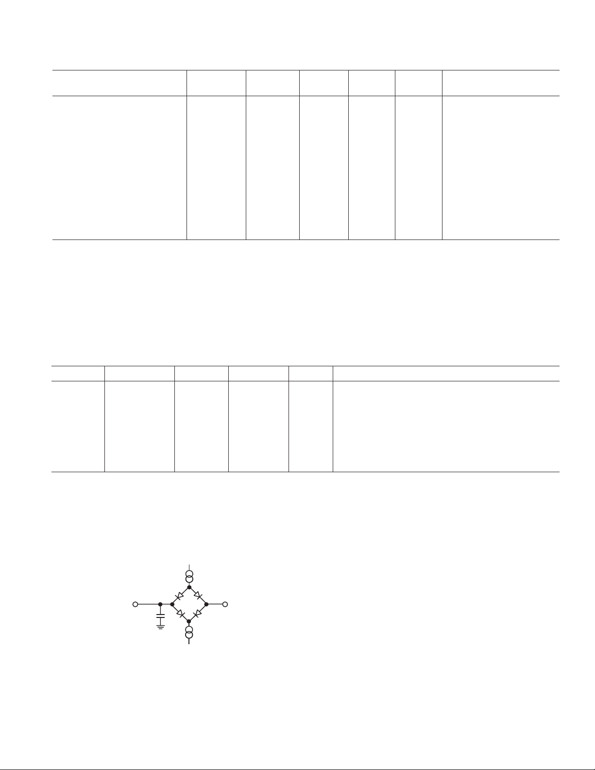
Measured with the load circuit of Figure 1 and defined as the time required for an output to cross 0.8 V or 2 V.
4
Derived from the measured time taken by the data outputs to change 0.5 V when loaded with the circuit of Figure 1. The measured number is then extrapolated back
to remove the effects of charging or discharging the 50 pF capacitor. This means that the time, t
of the part and as such is independent of external bus loading capacitances.
40 40 40 ns min CONVST Pulsewidth
2
40
2
40
3
60
3
100
10 10 10 ns min Data Hold Time after Falling Edge of SCLK
4
50
TO
OUTPUT
PIN
50pF
40
40
60
100
50
2
2
3
4
3
1.6mA
400A
1.6V
45
45
70
110
50
2
2
3
3
4
ns min SCLK High Pulsewidth
ns min SCLK Low Pulsewidth
Data Access Time after Falling Edge of SCLK
ns max VDD = 5 V ± 10%
ns max VDD = 2.7 V to 3.6 V
ns max Bus Relinquish Time after Falling Edge of SCLK
, and the setup time required for the user’s
4
, quoted in the timing characteristics is the true bus relinquish time
6
Figure 1. Load Circuit for Access Time and Bus
Relinquish Time
REV. C
–3–

AD7896
ABSOLUTE MAXIMUM RATINGS*
(TA = 25°C, unless otherwise noted.)
V
to AGND . . . . . . . . . . . . . . . . . . . . . . . . . . –0.3 V to +7 V
DD
to DGND . . . . . . . . . . . . . . . . . . . . . . . . . . –0.3 V to +7 V
V
DD
Analog Input Voltage to AGND . . . . . . –0.3 V to V
Digital Input Voltage to DGND . . . . . . –0.3 V to V
Digital Output Voltage to DGND . . . . . –0.3 V to V
+ 0.3 V
DD
+ 0.3 V
DD
+ 0.3 V
DD
Operating Temperature Range
Commercial (J Version) . . . . . . . . . . . . . . . . . 0°C to +70°C
Industrial (A, B Versions) . . . . . . . . . . . . . . –40°C to +85°C
Extended (S Version) . . . . . . . . . . . . . . . . . –55°C to +125°C
Storage Temperature Range . . . . . . . . . . . . . –65°C to +150°C
Junction Temperature . . . . . . . . . . . . . . . . . . . . . . . . . . 150°C
ORDERING GUIDE
Temperature Linearity SNR Package
Model Range Error (LSB) (dB) Option*
AD7896AN –40°C to +85°C ± 170N-8
AD7896BN –40°C to +85°C ± 1/2 70 N-8
AD7896AR –40°C to +85°C ± 170R-8
AD7896AR-REEL –40°C to +85°C ± 170R-8
AD7896AR-REEL7 –40°C to +85°C ± 170R-8
AD7896BR –40°C to +85°C ± 1/2 70 R-8
AD7896BR-REEL –40°C to +85°C ± 1/2 70 R-8
AD7896BR-REEL7 –40°C to +85°C ± 1/2 70 R-8
AD7896JR 0°C to +70°C ±170R-8
AD7896JR-REEL 0°C to +70°C ±170R-8
AD7896SQ –55°C to +125°C ± 170Q-8
EVAL-AD7896CB Evaluation Board
*N = PDIP; Q = CERDIP; R = SOIC.
PDIP Package, Power Dissipation . . . . . . . . . . . . . . . . 450 mW
Thermal Impedance . . . . . . . . . . . . . . . . . . . . . 125°C/W
JA
Thermal Impedance . . . . . . . . . . . . . . . . . . . . . . 50°C/W
JC
Lead Temperature (Soldering, 10 sec) . . . . . . . . . . . . 260°C
SOIC Package, Power Dissipation . . . . . . . . . . . . . . . .450 mW
Thermal Impedance . . . . . . . . . . . . . . . . . . . . . 160°C/W
JA
Thermal Impedance . . . . . . . . . . . . . . . . . . . . . . 75°C/W
JC
Lead Temperature, Soldering
Vapor Phase (60 sec) . . . . . . . . . . . . . . . . . . . . . . . 215°C
Infrared (15 sec) . . . . . . . . . . . . . . . . . . . . . . . . . . . 220°C
ESD . . . . . . . . . . . . . . . . . . . . . . . . . . . . . . . . . . . . .>4000 V
*Stresses above those listed under Absolute Maximum Ratings may cause perma-
nent damage to the device. This is a stress rating only; functional operation of the
device at these or any other conditions above those listed in the operational
sections of this specification is not implied. Exposure to absolute maximum rating
conditions for extended periods may affect device reliability.
CAUTION
ESD (electrostatic discharge) sensitive device. Electrostatic charges as high as 4000 V readily
accumulate on the human body and test equipment and can discharge without detection. Although the
AD7896 features proprietary ESD protection circuitry, permanent damage may occur on devices
subjected to high energy electrostatic discharges. Therefore, proper ESD precautions are recommended
to avoid performance degradation or loss of functionality.
REV. C–4–

PIN CONFIGURATION
T
AD7896
V
V
AGND
SCLK
1
IN
2
DD
3
4
AD7896
TOP VIEW
(Not to Scale)
8
7
6
5
BUSY
CONVS
DGND
SDATA
PIN FUNCTION DESCRIPTIONS
Pin No. Mnemonic Description
1V
2V
IN
DD
Analog Input. The analog input range is 0 V to VDD.
Positive supply voltage, 2.7 V to 5.5 V.
3 AGND Analog Ground. Ground reference for track-and-hold, comparator, and DAC.
4 SCLK Serial Clock Input. An external serial clock is applied to this input to obtain serial data from the AD7896.
A new serial data bit is clocked out on the falling edge of this serial clock. Data is guaranteed valid for
10 ns after this falling edge so data can be accepted on the falling edge when a fast serial clock is used.
The serial clock input should be taken low at the end of the serial data transmission.
5 SDATA Serial Data Output. Serial data from the AD7896 is provided at this output. The serial data is clocked
out by the falling edge of SCLK, but the data can also be read on the falling edge of the SCLK. This is
possible because data bit N is valid for a specified time after the falling edge of the SCLK (data hold
time) and can be read before data bit N+1 becomes valid a specified time after the falling edge of SCLK
(data access time) (see Figure 4). Sixteen bits of serial data are provided with four leading zeros followed
by the 12 bits of conversion data. On the 16th falling edge of SCLK, the SDATA line is held for the data
hold time and then disabled (three-stated). Output data coding is straight binary.
6 DGND Digital Ground. Ground reference for digital circuitry.
7 CONVST Convert Start. Edge-triggered logic input. On the falling edge of this input, the track-and-hold goes into
its hold mode and conversion is initiated. If CONVST is low at the end of conversion, the part goes into
power-down mode. In this case, the rising edge of CONVST “wakes up” the part.
8 BUSY The BUSY pin is used to indicate when the part is doing a conversion. The BUSY pin goes high on the
falling edge of CONVST and returns low when the conversion is complete.
REV. C
–5–
 Loading...