

2.7 V to 5.25 V, Micropower, 8-Channel,
SAR + ADC
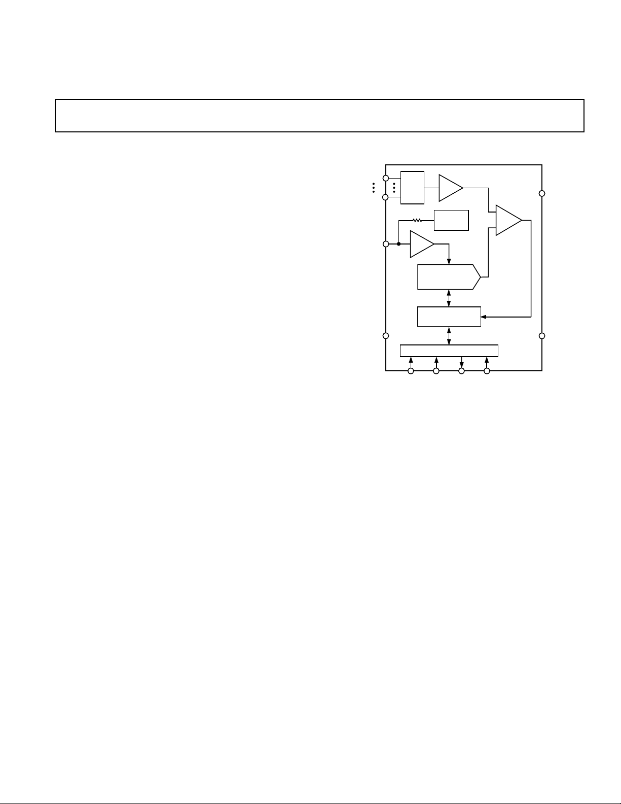
CONTROL LOGIC
AGND
REF IN/REF OUT
AIN8
AIN1
SCLK
DOUT
DIN
AGND
AD7888
V
DD
CS
T/H
I/P
MUX
BUF
2.5V
REF
CHARGE
REDISTRIBUTION
DAC
SPORT
COMP
a
125 kSPS, 12-Bit ADC in 16-Lead TSSOP
FEATURES
Specified for V
of 2.7 V to 5.25 V
DD
Flexible Power/Throughput Rate Management
Shutdown Mode: 1 A Max
Eight Single-Ended Inputs
Serial Interface: SPI™/QSPI™/MICROWIRE™/DSP
Compatible
16-Lead Narrow SOIC and TSSOP Packages
APPLICATIONS
Battery-Powered Systems (Personal Digital Assistants,
Medical Instruments, Mobile Communications)
Instrumentation and Control Systems
High-Speed Modems
GENERAL DESCRIPTION
The AD7888 is a high speed, low power, 12-bit ADC that operates from a single 2.7 V to 5.25 V power supply. The AD7888 is
capable of a 125 kSPS throughput rate. The input track-andhold acquires a signal in 500 ns and features a single-ended
sampling scheme. The AD7888 contains eight single-ended
analog inputs, AIN1 through AIN8. The analog input on each
of these channels is from 0 to V
. The part is capable of con-
REF
verting full power signals up to 2.5 MHz.
The AD7888 features an on-chip 2.5 V reference that can be
used as the reference source for the A/D converter. The REF
IN/REF OUT pin allows the user access to this reference. Alternatively, this pin can be overdriven to provide an external reference voltage for the AD7888. The voltage range for this external
reference is from 1.2 V to V
DD
.
CMOS construction ensures low power dissipation of typically
2 mW for normal operation and 3 µW in power-down mode.
The part is available in a 16-lead narrow body small outline
(SOIC) and a 16-lead thin shrink small outline (TSSOP) package.
AD7888
FUNCTIONAL BLOCK DIAGRAM
PRODUCT HIGHLIGHTS
1. Smallest 12-bit 8-channel ADC; 16-lead TSSOP is the same
area as an 8-lead SOIC and less than half the height.
2. Lowest Power 12-bit 8-channel ADC.
3. Flexible power management options including automatic
power-down after conversion.
4. Analog input range from 0 V to V
5. Versatile serial I/O port (SPI/QSPI/MICROWIRE/DSP
Compatible).
REF
(VDD).
SPI and QSPI are trademarks of Motorola, Inc.
MICROWIRE is a trademark of National Semiconductor Corporation.
REV. B
Information furnished by Analog Devices is believed to be accurate and
reliable. However, no responsibility is assumed by Analog Devices for its
use, nor for any infringements of patents or other rights of third parties that
may result from its use. No license is granted by implication or otherwise
under any patent or patent rights of Analog Devices.
One Technology Way, P.O. Box 9106, Norwood, MA 02062-9106, U.S.A.
Tel: 781/329-4700 www.analog.com
Fax: 781/326-8703 © Analog Devices, Inc., 2001

AD7888–SPECIFICATIONS
otherwise noted; f
Parameter A Version1B Version
DYNAMIC PERFORMANCE
Signal to Noise + Distortion Ratio
Total Harmonic Distortion
Peak Harmonic or Spurious Noise
= 2 MHz (VDD = 2.7 V to 5.25 V); TA = T
SCLK
2, 3
(SNR) 71 71 dB typ fIN = 10 kHz Sine Wave, f
2
(THD) –80 –80 dB typ fIN = 10 kHz Sine Wave, f
2
–80 –80 dB typ fIN = 10 kHz Sine Wave, f
(VDD = 2.7 V to 5.25 V, REFIN/REFOUT = 2.5 V External/Internal Reference unless
to T
MIN
, unless otherwise noted.)
MAX
1
Unit Test Condition/Comment
SAMPLE
SAMPLE
SAMPLE
= 125 kSPS
= 125 kSPS
= 125 kSPS
Intermodulation Distortion2 (IMD)
Second Order Terms –78 –78 dB typ fa = 9.983 kHz, fb = 10.05 kHz, f
Third Order Terms –78 –78 dB typ fa = 9.983 kHz, fb = 10.05 kHz, f
Channel-to-Channel Isolation
2
–80 –80 dB typ fIN = 25 kHz
SAMPLE
SAMPLE
= 125 kSPS
= 125 kSPS
Full Power Bandwidth 2.5 2.5 MHz typ @ 3 dB
DC ACCURACY Any Channel
Resolution 12 12 Bits
Integral Nonlinearity
Differential Nonlinearity
2
2
± 2 ± 1 LSB max
± 2 –1/+1.5 LSB max Guaranteed No Missed Codes to 11 Bits (A Grade)
Guaranteed No Missed Codes to 12 Bits (B Grade)
Offset Error ± 6 ± 6 LSB max V
± 4.5 ±4.5 LSB max V
2 2 LSB typ
± 2 ± 2 LSB max Typically 30 LSB with Internal Reference
3 3 LSB max
Offset Error Match
Gain Error
Gain Error Match
2
2
2
= 4.75 V to 5.25 V (Typically ±3 LSB)
DD
= 2.7 V to 3.6 V (Typically ±2 LSB)
DD
ANALOG INPUT
Input Voltage Ranges 0 to V
REF
0 to V
REF
Volts
Leakage Current ± 1 ± 1 µA max
Input Capacitance 38 38 pF typ When in Track
4 4 pF typ When in Hold
REFERENCE INPUT/OUTPUT
REFIN Input Voltage Range 2.5/V
DD
2.5/V
DD
V min/max Functional from 1.2 V
Input Impedance 5 5 kΩ typ Very High Impedance If Internal Reference Disabled
REFOUT Output Voltage 2.45/2.55 2.45/2.55 V min/max
REFOUT Tempco ± 50 ± 50 ppm/°C typ
LOGIC INPUTS
Input High Voltage, V
INH
2.4 2.4 V min VDD = 4.75 V to 5.25 V
2.1 2.1 V min VDD = 2.7 V to 3.6 V
Input Low Voltage, V
Input Current, I
IN
Input Capacitance, C
IN
INL
4
0.8 0.8 V max VDD = 2.7 V to 5.25 V
± 10 ± 10 µA max Typically 10 nA, VIN = 0 V or V
10 10 pF max
DD
LOGIC OUTPUTS
Output High Voltage, V
OH
I
SOURCE
= 200 µA
VDD – 0.5 VDD – 0.5 V min VDD = 2.7 V to 5.25 V
Output Low Voltage, V
Floating-State Leakage Current ± 10 ± 10 µA max
Floating-State Output Capacitance
OL
5
0.4 0.4 V max I
10 10 pF max
SINK
= 200 µA
Output Coding Straight (Natural) Binary
CONVERSION RATE
Throughput Time 16 16 SCLK Cycles Conversion Time + Acquisition Time. 125 kSPS with
2 MHz Clock
Track/Hold Acquisition Time
2
1.5 1.5 SCLK Cycles
Conversion Time 14.5 14.5 SCLK Cycles 7.25 µs (2 MHz Clock)
–2–
REV. B
Parameter A Version1B Version
WARNING!
ESD SENSITIVE DEVICE
1
Unit Test Condition/Comment
POWER REQUIREMENTS
V
DD
I
DD
Normal Mode5 (Static) 700 700 µA max
Normal Mode
(Operational) 700 700 µA typ f
Using Standby Mode 450 450 µA typ f
Using Shutdown Mode 80 80 µA typ f
Standby Mode
Shutdown Mode
6
6
Normal-Mode Power Dissipation 3.5 3.5 mW max V
2.7/5.25 2.7/5.25 V min/max
= 125 kSPS
SAMPLE
= 50 kSPS
SAMPLE
= 10 kSPS
SAMPLE
12 12 µA typ f
SAMPLE
= 1 kSPS
200 200 µA max VDD = 2.7 V to 5.25 V
22 µA max VDD = 4.75 V to 5.25 V (0.5 µA typ)
11 µA max V
= 2.7 V to 3.6 V
DD
= 5 V
DD
2.1 2.1 mW max VDD = 3 V
Shutdown Power Dissipation 10 10 µW max V
33 µW max V
DD
DD
= 5 V
= 3 V
Standby Power Dissipation 1 1 mW max VDD = 5 V
600 600 µW max VDD = 3 V
NOTES
1
Temperature ranges as follows: A Version: –40°C to +105°C; B Version: –40°C to +105°C.
2
See Terminology.
3
SNR calculation includes distortion and noise components.
4
Sample tested @ 25°C to ensure compliance.
5
All digital inputs @ GND except CS @ VDD. No load on the digital outputs. Analog inputs @ GND.
6
SCLK @ GND when SCLK off. All digital inputs @ GND except for CS @ VDD. No load on the digital outputs. Analog inputs @ GND.
Specifications subject to change without notice.
AD7888
ABSOLUTE MAXIMUM RATINGS
1
(TA = 25°C unless otherwise noted)
VDD to AGND . . . . . . . . . . . . . . . . . . . . . . . . . –0.3 V to +7 V
Analog Input Voltage to AGND . . . . . –0.3 V to V
Digital Input Voltage to AGND . . . . . . –0.3 V to V
Digital Output Voltage to AGND . . . . –0.3 V to V
REFIN/REFOUT to AGND . . . . . . . . –0.3 V to V
Input Current to Any Pin Except Supplies
2
. . . . . . . . ± 10 mA
+ 0.3 V
DD
+ 0.3 V
DD
+ 0.3 V
DD
+ 0.3 V
DD
Operating Temperature Range
Commercial
(A Version) . . . . . . . . . . . . . . . . . . . . . . –40°C to +105°C
(B Version) . . . . . . . . . . . . . . . . . . . . . . . 0°C to +105°C
Storage Temperature Range . . . . . . . . . . . –65°C to +150°C
Junction Temperature . . . . . . . . . . . . . . . . . . . . . . . . . 150°C
SOIC, TSSOP Package, Power Dissipation . . . . . . . . 450 mW
Thermal Impedance . . . . . . . . . . . . 124.9°C/W (SOIC)
θ
JA
. . . . . . . . . . . . . . . . . . . . . . . . . . . . . . 150.4°C/W (TSSOP)
Thermal Impedance . . . . . . . . . . . . . 42.9°C/W (SOIC)
θ
JC
. . . . . . . . . . . . . . . . . . . . . . . . . . . . . . . 27.6°C/W (TSSOP)
Lead Temperature, Soldering
Vapor Phase (60 secs) . . . . . . . . . . . . . . . . . . . . . . 215°C
Infrared (15 secs) . . . . . . . . . . . . . . . . . . . . . . . . . 220°C
ESD . . . . . . . . . . . . . . . . . . . . . . . . . . . . . . . . . . . . . . . . . 1 kV
NOTES
1
Stresses above those listed under Absolute Maximum Ratings may cause perma-
nent damage to the device. This is a stress rating only; functional operation of the
device at these or any other conditions above those listed in the operational
sections of this specification is not implied. Exposure to absolute maximum rating
conditions for extended periods may affect device reliability.
2
Transient currents of up to 100 mA will not cause SCR latch-up.
ORDERING GUIDE
Linearity
Error Package Package
Model (LSB)1Description Option
AD7888AR ± 2 SOIC R-16A
AD7888BR ± 1 SOIC R-16A
AD7888ARU ± 2 TSSOP RU-16
AD7888BRU ± 1 TSSOP RU-16
EVAL-AD7888CB
EVAL-CONTROL BRD2
NOTES
1
Linearity error here refers to integral linearity error.
2
This can be used as a stand-alone evaluation board or in conjunction with the
EVAL-CONTROL BOARD for evaluation/demonstration purposes.
3
This board is a complete unit allowing a PC to control and communicate with all
Analog Devices evaluation boards ending in the CB designators.
2
3
CAUTION
ESD (electrostatic discharge) sensitive device. Electrostatic charges as high as 4000 V readily
accumulate on the human body and test equipment and can discharge without detection.
Although the AD7888 features proprietary ESD protection circuitry, permanent damage may
occur on devices subjected to high-energy electrostatic discharges. Therefore, proper ESD
precautions are recommended to avoid performance degradation or loss of functionality.
REV. B –3–
AD7888
TIMING SPECIFICATIONS
1
(TA = T
MIN
to T
, unless otherwise noted)
MAX
Limit at T
MIN
, T
MAX
(A, B Versions)
Parameter 4.75 V to 5.25 V 2.7 V to 3.6 V Unit Description
2
f
SCLK
t
CONVERT
t
ACQ
t
1
3
t
2
3
t
3
t
4
t
5
t
6
t
7
4
t
8
t
9
NOTES
1
Sample tested at 25°C to ensure compliance. All input signals are specified with tr = tf = 5 ns (10% to 90% of VDD) and timed from a voltage level of 1.6 V.
2
Mark/Space ratio for the SCLK input is 40/60 to 60/40. See Serial Interface section.
3
Measured with the load circuit of Figure 1 and defined as the time required for the output to cross 0.8 V or 2.4 V with V
cross 0.4 V or 2.0 V with VDD = 3 V ± 10%.
4
t8 is derived from the measured time taken by the data outputs to change 0.5 V when loaded with the circuit of Figure 1. The measured number is then extrapolated
back to remove the effects of charging or discharging the 50 pF capacitor. This means that the time, t
time of the part and is independent of the bus loading.
Specifications subject to change without notice.
2 2 MHz max
14.5 t
1.5 t
SCLK
SCLK
14.5 t
1.5 t
SCLK
SCLK
Throughput Time = t
CONVERT
+ t
ACQ
= 16 t
SCLK
10 10 ns min CS to SCLK Setup Time
30 60 ns max Delay from CS until DOUT 3-State Disabled
75 100 ns max Data Access Time after SCLK Falling Edge
20 20 ns min Data Setup Time Prior to SCLK Rising Edge
20 20 ns min Data Valid to SCLK Hold Time
0.4 t
0.4 t
SCLK
SCLK
0.4 t
0.4 t
SCLK
SCLK
ns min SCLK High Pulsewidth
ns min SCLK Low Pulsewidth
80 80 ns max CS Rising Edge to DOUT High Impedance
55µs typ Power-Up Time from Shutdown
= 5 V ± 10% and time for an output to
DD
, quoted in the timing characteristics is the true bus relinquish
8
I
OL
1.6V
I
OH
OUTPUT
PIN
TO
50pF
200A
C
L
200A
Figure 1. Load Circuit for Digital Output Timing Specifications
–4–
REV. B
PIN CONFIGURATIONS
SOIC AND TSSOP
AD7888
CS
REF IN/REF OUT
V
AGND
AIN1
AIN2
AIN3
AIN4
DD
1
2
3
AD7888
4
TOP VIEW
5
(Not to Scale)
6
7
8
16
SCLK
15
DOUT
14
DIN
13
AGND
12
AIN8
11
AIN7
10
AIN6
9
AIN5
PIN FUNCTION DESCRIPTIONS
Pin
No. Mnemonic Function
1 CS Chip Select. Active low logic input. This input provides the dual function of initiating conversions on
the AD7888 and also frames the serial data transfer.
2 REF IN/REF OUT Reference Input/Output. The on-chip reference is available on this pin for use external to the AD7888.
Alternatively, the internal reference can be disabled and an external reference applied to this input.
3V
DD
The voltage range for the external reference is from 1.2 V to V
Power Supply Input. The VDD range for the AD7888 is from 2.7 V to 5.25 V.
DD
.
4, 13 AGND Analog Ground. Ground reference point for all circuitry on the AD7888. All analog input signals and
any external reference signals should be referred to this AGND voltage. Both of these pins should
connect to the AGND plane of a system.
5–12 AIN1–AIN8 Analog Input 1 through Analog Input 8. Eight single-ended analog input channels that are multiplexed
into the on-chip track/hold. The analog input channel to be converted is selected by using the ADD0
through ADD2 bits of the Control Register. The input range for all input channels is 0 to V
REF
. Any
unused input channels should be connected to AGND to avoid noise pickup.
14 DIN Data In. Logic Input. Data to be written to the AD7888’s Control Register is provided on this input
and is clocked into the register on the rising edge of SCLK (see Control Register section).
15 DOUT Data Out. Logic Output. The conversion result from the AD7888 is provided on this output as a serial
data stream. The bits are clocked out on the falling edge of the SCLK input. The data stream consists
of four leading zeros followed by the 12 bits of conversion data, which is provided MSB first.
16 SCLK Serial Clock. Logic Input. SCLK provides the serial clock for accessing data from the part and writing
serial data to the Control Register. This clock input is also used as the clock source for the AD7888’s
conversion process.
REV. B
–5–

AD7888
TERMINOLOGY
Integral Nonlinearity
This is the maximum deviation from a straight line passing
through the endpoints of the ADC transfer function. The endpoints of the transfer function are zero scale, a point 1/2 LSB
below the first code transition, and full scale, a point 1/2 LSB
above the last code transition.
Differential Nonlinearity
This is the difference between the measured and the ideal 1 LSB
change between any two adjacent codes in the ADC.
Offset Error
This is the deviation of the first code transition (00 . . . 000) to
(00 . . . 001) from the ideal, i.e., AGND + 0.5 LSB.
Offset Error Match
This is the difference in offset error between any two channels.
Gain Error
This is the deviation of the last code transition (111 . . . 110) to
(111 . . . 111) from the ideal (i.e., V
– 1.5 LSB) after the
REF
offset error has been adjusted out.
Gain Error Match
This is the difference in gain error between any two channels.
Track/Hold Acquisition Time
The track/hold amplifier returns into track mode at the end of
conversion. Track/Hold acquisition time is the time required for
the output of the track/hold amplifier to reach its final value,
within ± 1/2 LSB, after the end of conversion.
Signal to (Noise + Distortion) Ratio
This is the measured ratio of signal to (noise + distortion) at the
output of the A/D converter. The signal is the rms amplitude of
the fundamental. Noise is the sum of all nonfundamental signals up to half the sampling frequency (f
/2), excluding dc. The
S
ratio is dependent on the number of quantization levels in the
digitization process; the more levels, the smaller the quantization noise. The theoretical signal to (noise + distortion) ratio for
an ideal N-bit converter with a sine wave input is given by:
Signal to (Noise + Distortion) = (6.02 N + 1.76) dB
Thus for a 12-bit converter, this is 74 dB.
Total Harmonic Distortion
Total harmonic distortion (THD) is the ratio of the rms sum of
harmonics to the fundamental. For the AD7888, it is defined as:
Peak Harmonic or Spurious Noise
Peak harmonic or spurious noise is defined as the ratio of the
rms value of the next largest component in the ADC output
spectrum (up to f
/2 and excluding dc) to the rms value of the
S
fundamental. Normally, the value of this specification is determined by the largest harmonic in the spectrum, but for ADCs
where the harmonics are buried in the noise floor, it will be a
noise peak.
Intermodulation Distortion
With inputs consisting of sine waves at two frequencies, fa and
fb, any active device with nonlinearities will create distortion
products at sum and difference frequencies of mfa ± nfb where
m, n = 0, 1, 2, 3, etc. Intermodulation distortion terms are
those for which neither m nor n is equal to zero. For example,
the second order terms include (fa + fb) and (fa – fb), while the
third order terms include (2fa + fb), (2fa – fb), (fa + 2fb) and
(fa – 2fb).
The AD7888 is tested using the CCIF standard where two
input frequencies near the top end of the input bandwidth are
used. In this case, the second order terms are usually distanced
in frequency from the original sine waves while the third order
terms are usually at a frequency close to the input frequencies.
As a result, the second and third order terms are specified separately. The calculation of the intermodulation distortion is as
per the THD specification where it is the ratio of the rms sum of
the individual distortion products to the rms amplitude of the
sum of the fundamentals expressed in dBs.
Channel-to-Channel Isolation
Channel-to-channel isolation is a measure of the level of crosstalk
between channels. It is measured by applying a full-scale 25 kHz
sine wave signal to all nonselected input channels and determining how much that signal is attenuated in the selected channel.
The figure given is the worst case across all four or eight channels for the AD7888.
PSR (Power Supply Rejection)
Variations in power supply will affect the full-scale transition,
but not the converter’s linearity. Power supply rejection is the
maximum change in the full-scale transition point due to a
change in power-supply voltage from the nominal value.
2
THD dB
( ) log=
VVVVV
++++
223242526
V
1
where V1 is the rms amplitude of the fundamental and V2, V3,
V
, V5 and V6 are the rms amplitudes of the second through the
4
sixth harmonics.
–6–
REV. B

AD7888
71.0
0 42.14
SNR – dB
73.0
72.5
72.0
71.5
10.89 31.59
VDD = 5V
5V EXT REFERENCE
21.14
INPUT FREQUENCY – kHz
CONTROL REGISTER
The Control Register on the AD7888 is an 8-bit, write-only register. Data is loaded from the DIN pin of the AD7888 on the rising
edge of SCLK. The data is transferred on the DIN line at the same time as the conversion result is read from the part. This requires
16 serial clocks for every data transfer. Only the information provided on the first 8 rising clock edges (after CS falling edge) is loaded
to the Control Register. MSB denotes the first bit in the data stream. The bit functions are outlined in Table I. The default contents
of the Control Register on power-up is all zeros.
Table I. Control Register Bit Function Description
MSB
CTNODOREZ2DDA1DDA0DDAFER1MP0MP
Bit Mnemonic Comment
7 DONTC Don’t Care. The value written to this bit of the Control Register is a don’t care, i.e., it doesn’t matter if the bit is
0 or 1.
6 ZERO A zero must be written to this bit to ensure correct operation of the AD7888.
5 ADD2 These three address bits are loaded at the end of the present conversion sequence and select which analog input
4 ADD1 channel is converted for the next conversion. The selected input channel is decoded as shown in Table II.
3 ADD0
2 REF Reference Bit. With a 0 in this bit, the on-chip reference is enabled. With a 1 in this bit, the on-chip reference
is disabled. To obtain best performance from the AD7888, the internal reference should be disabled when
using an externally applied reference source. (See On-Chip Reference section.)
1, 0 PM1, PM0 Power Management Bits. These two bits decode the mode of operation of the AD7888 as shown in Table III.
PERFORMANCE CURVES
Figure 2 shows a typical FFT plot for the AD7888 at 100 kHz
sample rate and 10 kHz input frequency.
–10
–30
–50
dB
–70
–90
–110
0 48.83
12.21 24.41 36.62
FREQUENCY – kHz
4096 POINT FFT
SAMPLING
100kSPS
f
= 10kHz
IN
SNR = 70dB
Figure 2. Dynamic Performance
Figure 3 shows a typical plot for the SNR vs. frequency for a
5 V supply and with a 5 V external reference.
Figure 3. SNR vs. Input Frequency
REV. B
–7–

AD7888
Figure 4 shows the typical power supply rejection ratio vs.
frequency for the part. The power supply rejection ratio is defined
as the ratio of the power in the ADC output at frequency f
to the power of a full-scale sine wave applied to the ADC of
frequency fs:
PSRR (dB) = 10 log (Pf/Pfs)
Pf = Power at frequency f in ADC output, Pfs = power at fre-
quency fs in ADC full scale input. Here a 100 mV peak-to-peak
sine wave is coupled onto the V
supply. Both the 2.7 V and
DD
5.5 V supply performances are shown.
–75
VDD = 5.5V/ 2.7V
–77
100mV p-p SINE WAVE ON V
REFIN = 2.488V EXT REFERENCE
–79
–81
–83
–85
PSRR – dB
–87
–89
–91
–93
2.65
12.85 33.65
23.15
INPUT FREQUENCY – kHz
DD
43.85
54.35
64.15
Figure 4. PSRR vs. Frequency
CHARGE
REDISTRIBUTION
DAC
SAMPLING
CAPACITOR
A
AIN
SW1
AGND
(REF IN/REF OUT)/2
B
ACQUISITION
PHASE
SW2
COMPARATOR
CONTROL
LOGIC
Figure 5. ADC Acquisition Phase
When the ADC starts a conversion, (see Figure 6), SW2 will open
and SW1 will move to Position B causing the comparator to
become unbalanced. The control logic and the charge redistribution DAC are used to add and subtract fixed amounts of charge
from the sampling capacitor to bring the comparator back into a
balanced condition. When the comparator is rebalanced, the
conversion is complete. The control logic generates the ADC
output code. Figure 7 shows the ADC transfer function.
CHARGE
REDISTRIBUTION
DAC
SAMPLING
CAPACITOR
A
VIN
SW1
AGND
(REF IN/REF OUT)/2
B
CONVERSION
PHASE
SW2
COMPARATOR
CONTROL
LOGIC
CIRCUIT INFORMATION
The AD7888 is a fast, low power, 12-bit, single supply, 8-channel
A/D converter. The part can be operated from 3 V (2.7 V to
3.6 V) supply or from 5 V (4.75 V to 5.25 V) supply. When
operated from either a 5 V supply or a 3 V supply, the AD7888
is capable of throughput rates of 125 kSPS when provided with
a 2 MHz clock.
The AD7888 provides the user with an 8-channel multiplexer,
on-chip track/hold, A/D converter, reference and serial interface
housed in a tiny 16-lead TSSOP package, which offers the user
considerable space saving advantages over alternative solutions.
The serial clock input accesses data from the part and also
provides the clock source for the successive-approximation
A/D converter. The analog input range is 0 to V
the externally-applied V
can be between 1.2 V and VDD).
REF
REF
(where
The 8-channel multiplexer is controlled by the part’s Control
Register. This Control Register also allows the user to power-off
the internal reference and to determine the Modes of Operation.
CONVERTER OPERATION
The AD7888 is a successive-approximation analog-to-digital
converter based around a charge redistribution DAC. Figures 5
and 6 show simplified schematics of the ADC. Figure 5 shows
the ADC during its acquisition phase. SW2 is closed and SW1 is
in Position A, the comparator is held in a balanced condition
and the sampling capacitor acquires the signal on AIN.
Figure 6. ADC Conversion Phase
ADC TRANSFER FUNCTION
The output coding of the AD7888 is straight binary. The
designed code transitions occur at successive integer LSB
values (i.e., 1 LSB, 2 LSBs, etc.). The LSB size is = V
REF
/
4096. The ideal transfer characteristic for the AD7888 is
shown in Figure 7 below.
111...111
111...110
111...000
ADC CODE
011...111
000...010
000...001
000...000
0V
0.5LSB
1LSB = V
ANALOG INPUT
REF
/4096
+V
REF
– 1.5LSB
Figure 7. Transfer Characteristic
–8–
REV. B

AD7888
TYPICAL CONNECTION DIAGRAM
Figure 8 shows a typical connection diagram for the AD7888.
Both AGND pins are connected to the analog ground plane of
the system. V
provide an analog input range of 0 V to V
is connected to a well decoupled VDD pin to
REF
. The conversion
DD
result is output in a 16-bit word with four leading zeroes followed by the MSB of the 12-bit result. For applications where
power consumption is of concern, the automatic power down at
the end of conversion should be used to improve power performance. See Modes of Operation section of the data sheet.
SUPPLY 2.7V
TO 5.25V
0V TO
REF IN/
REF OUT
INPUT
10F
0.1F
AIN1
AIN2
AIN8
AGND
AGND
V
DD
AD7888
REF IN/
REF OUT
SCLK
DOUT
DIN
CS
SERIAL
INTERFACE
C/P
Figure 8. Typical Connection Diagram
Analog Input
Figure 9 shows an equivalent circuit of the analog input structure
of the AD7888. The two diodes D1 and D2 provide ESD protection for the analog inputs. Care must be taken to ensure that
the analog input signal never exceeds the supply rails by more
than 200 mV. This will cause these diodes to become forwardbiased and start conducting current into the substrate. 20 mA is
the maximum current these diodes can conduct without causing
irreversible damage to the part. However, it is worth noting that
a small amount of current (1 mA) being conducted into the
substrate due to an overvoltage on an unselected channel, can
cause inaccurate conversions on a selected channel. The capacitor C1 in Figure 9 is typically about 4 pF and can primarily be
attributed to pin capacitance. The resistor R1 is a lumped component made up of the on resistance of a multiplexer and a switch.
This resistor is typically about 100 Ω. The capacitor C2 is the
ADC sampling capacitor and has a capacitance of 20 pF typically.
Note: The analog input capacitance seen when the track and
hold is in track mode is typically 38 pF, while in hold mode it is
typically 4 pF.
V
DD
D1
V
IN
C1
4pF
D2
CONVERSION PHASE – SWITCH OPEN
TRACK PHASE – SWITCH CLOSED
R1
C2
20pF
Figure 9. Equivalent Analog Input Circuit
For ac applications, removing high frequency components from
the analog input signal is recommended by use of an RC lowpass filter on the relevant analog input pin. In applications
where harmonic distortion and signal to noise ratio are critical
the analog input should be driven from a low impedance source.
Large source impedances will significantly affect the ac performance of the ADC. This may necessitate the use of an input
buffer amplifier. The choice of the op amp will be a function of
the particular application.
When no amplifier is used to drive the analog input the source
impedance should be limited to low values. The maximum
source impedance will depend on the amount of total harmonic
distortion (THD) that can be tolerated. The THD will increase
as the source impedance increases and performance will degrade.
Figure 10 shows a graph of the total harmonic distortion versus
analog input signal frequency for different source impedances.
–65
THD vs. FREQUENCY FOR DIFFERENT
SOURCE IMPEDANCES
VDD = 5V
–70
5V EXT REFERENCE
–75
THD – dB
–80
–85
–90
0.15 42.14
RIN = 10⍀, CIN = 10nF
10.89 31.5921.14
INPUT FREQUENCY – kHz
RIN = 1k⍀, CIN = 100pF
RIN = 50⍀, CIN = 2.2nF
49.86
Figure 10. THD vs. Analog Input Frequency
Analog Input Selection
On power-up, the default AIN selection is AIN1. When returning
to normal operation from power-down, the AIN selected will be
the same one that was selected prior to power-down being initiated. Table II below shows the multiplexer address corresponding to each analog input from AIN1 to AIN8 for the AD7888.
Table II. Channel Configurations
ADD2 ADD1 ADD0 Analog Input Channel
0 0 0 AIN1
0 0 1 AIN2
0 1 0 AIN3
0 1 1 AIN4
1 0 0 AIN5
1 0 1 AIN6
1 1 0 AIN7
1 1 1 AIN8
On-Chip Reference
The AD7888 has an on-chip 2.5 V reference. This reference can
be enabled or disabled by clearing or setting the REF bit in the
Control Register, respectively. If the on-chip reference is to
be used externally in a system, it must be buffered before it is
applied elsewhere. If an external reference is applied to the device,
the internal reference is automatically overdriven. However, in
REV. B
–9–

AD7888
order to obtain optimum performance from the device it is
advised to disable the internal reference by setting the REF bit
in the Control Register when an external reference is applied.
When the internal reference is disabled, SW1 in Figure 11 will
open and the input impedance seen at the REF IN/REF OUT
pin is the input impedance of the reference buffer, which is in
the region of giga Ω. When the reference is enabled, the input
impedance seen at the pin is typically 5 kΩ.
REF IN/REF OUT
SW1
5k⍀
2.5V
Figure 11. On-Chip Reference Circuitry
Table III. Power Management Options
PM1 PM0 Mode
00Normal Operation. In this mode, the AD7888
remains in full power mode regardless of the
status of any of the logic inputs. This mode
allows the fastest possible throughput rate from
the AD7888.
01Full Shutdown. In this mode, the AD7888 is
in full shutdown mode with all circuitry on the
AD7888, including the on-chip reference, entering its power-down mode. The AD7888 retains
the information in the control Register bits
while in full shutdown. The part remains in full
shutdown until these bits are changed.
10Autoshutdown. In this mode, the AD7888
automatically enters full shutdown mode at the
end of each conversion. Wake-up time from full
shutdown is 5 µs and the user should ensure that
5 µs have elapsed before attempting to perform
a valid conversion on the part in this mode.
11Autostandby. In this standby mode, portions
of the AD7888 are powered down but the onchip reference voltage remains powered up. The
REF bit should be 0 to ensure the on-chip reference is enabled. This mode is similar to autoshutdown but allows the part to power-up
much faster.
POWER-DOWN OPTIONS
The AD7888 provides flexible power management to allow the
user to achieve the best power performance for a given throughput rate.
The power management options are selected by programming
the power management bits (i.e., PM1 and PM0) in the control
register. Table III summarizes the options available. When the
power management bits are programmed for either of the auto
power-down modes, the part will enter the power-down mode
on the 16th rising SCLK edge after the falling edge of CS. The
first falling SCLK edge after the CS falling edge will cause the
part to power up again. When the AD7888 is in full shutdown,
the only way to fully power it up again is to reprogram the
power management bits to PM1 = PM0 = 0, i.e., normal
mode. In this case the device will power up on the 16th SCLK
rising edge after the CS falling edge as this is when the power
management bits become effective.
Power-Up Times
The AD7888 has an approximate 1 µs power-up time when
powering up from standby or when using an external reference.
When V
is first connected, the AD7888 will fully power up,
DD
i.e., it powers up in normal mode. If the part is put into shutdown, a subsequent power-up will take approximately 5 µs. The
AD7888 wake-up time is very short in the autostandby mode so
it is possible to wake up the part and carry out a valid conversion in the same read/write operation.
POWER vs. THROUGHPUT RATE
By operating the AD7888 in autoshutdown or autostandby
mode the average power consumption of the AD7888 decreases
at lower throughput rates. Figure 12 shows how as the throughput rate is reduced, the device remains in its power-down state
longer and the average power consumption over time drops
accordingly.
For example, if the AD7888 were operated in a continuous
sampling mode, with a throughput rate of 10 kSPS and a SCLK
of 2 MHz (V
= 5 V), and if PM1 = 1 and PM0 = 0, i.e., the
DD
device is in autoshutdown mode and the on-chip reference is
used, the power consumption is calculated as follows. The
power dissipation during normal operation is 3.5 mW (V
DD
=
5 V). If the power-up time is 5 µs and the remaining conversion-
plus-acquisition time is 15.5 t
, i.e., approximately 7.75 µs,
SCLK
(see Figure 14a), the AD7888 can be said to dissipate 3.5 mW
for 12.75 µs during each conversion cycle. If the throughput rate
is 10 kSPS, the cycle time is 100 µs and the average power dissi-
pated during each cycle is (12.75/100) × (3.5 mW) = 446.25 µW.
= 3 V SCLK = 2 MHz, and the device is again in auto-
If V
DD
shutdown mode using the on-chip reference, the power dissipation during normal operation is 2.1 mW. The AD7888 can now
be said to dissipate 2.1 mW for 12.75 µs during each conversion
cycle. With a throughput rate of 10 kSPS, the average power
dissipated during each cycle is (12.75/100) × (2.1 mW) =
267.75 µW. Figure 12 shows the power vs. throughput rate for
automatic shutdown with both 5 V and 3 V supplies.
10
VDD = 5V
SCLK = 2MHz
VDD = 3V
SCLK = 2MHz
10
THROUGHPUT – kSPS
20 30 40 50
POWER – mW
0.1
0.01
1
0
Figure 12. Power vs. Throughput
–10–
REV. B

CS
SCLK
4 LEADING ZEROES + CONVERSION RESULT
CS
DOUT
DATA IN
DIN
THE PART POWERS UP FROM
SHUTDOWN ON SCLK FALLING EDGE AS
PM1 = 1 AND PM0 = 0
1
16
4 LEADING ZEROES + CONVERSION RESULT
DATA IN
1162
t
10
= 5s
THE PART ENTERS
SHUTDOWN AT THE END OF
CONVERSION AS PM1 = 1 AND PM0 = 0
CONTROL REGISTER DATA IS LOADED ON THE
FIRST 8 CLOCKS. PM1 = 1 AND PM0 = 0
PM1 = 1 AND PM0 = 0 TO KEEP THE
PART IN THIS MODE
SCLK
THE PART REMAINS POWERED UP
AT ALL TIMES AS PM1 AND PM0 = 0
1
AD7888
16
DOUT
DIN
4 LEADING ZEROES + CONVERSION RESULT
DATA IN
CONTROL REGISTER DATA IS LOADED ON THE
FIRST 8 CLOCKS. PM1 AND PM0 = 0 TO KEEP
THE PART IN THIS MODE
Figure 13. Normal-Mode Operation
MODES OF OPERATION
The AD7888 has a number of different modes of operation.
These are designed to provide flexible power management
options. These options can be chosen to optimize the power
dissipation/throughput rate ratio for differing application requirements. The modes of operation are controlled by the PM1 and
PM0 bits of the Control Register as outlined previously.
Normal Mode (PM1 = 0, PM0 = 0)
This mode is intended for fastest throughput rate performance
as the user does not have to worry about any power-up times
with the AD7888 remaining fully powered all the time. Figure
13 shows the general diagram of the operation of the AD7888 in
this mode.
The data presented to the AD7888 on the DIN line during the
first eight clock cycles of the data transfer are loaded to the
Control Register. The part will remain powered up at the end of
the conversion as long as PM1 and PM0 were set to zero in the
write during that conversion. To continue to operate in this
mode, the user must ensure that PM1 and PM0 are both loaded
with 0 on every data transfer.
The falling edge of CS initiates the sequence and the input
signal is sampled on the second rising edge of the SCLK input.
Sixteen serial clock cycles are required to complete the conversion and access the conversion result. Once a data transfer is
complete (CS has returned high), another conversion can be
initiated immediately by bringing CS low again.
Full Shutdown (PM1 = 0, PM0 = 1)
In this mode, all internal circuitry on the AD7888, including the
on-chip reference, is powered-down. The part retains the information in the Control Register during full shutdown. The part
remains in full shutdown until the power management bits are
changed. If the power management bits are changed to PM1 = 1
and PM0 = 0, i.e., the autoshutdown mode, the part will remain
in shutdown (now in autoshutdown) but will power up once a
conversion is initiated after that (see Power-Up Times section).
The part changes mode as soon as the control register has been
updated, so if the part is in full shutdown mode and the power
management bits are changed to PM1 = PM0 = 0, i.e., normal
mode, then the part will power up on the 16th SCLK rising edge.
Autoshutdown (PM1 = 1, PM0 = 0)
In this mode, the AD7888 automatically enters its power-down
mode at the end of every conversion. Figure 14a shows the
general diagram of the operation of the AD7888 in this mode.
When CS goes from high to low, all on-chip circuitry will start
to power up on the next falling edge of SCLK. On the sixteenth
SCLK rising edge the part will power down again. It takes
approximately 5 µs for the AD7888 internal circuitry to be fully
powered up. As a result, a conversion (or sample-and-hold
acquisition) should not be initiated during this 5 µs. The input
signal is sampled on the second rising edge of SCLK following
the CS falling edge. The user should ensure that 5 µs elapse
between the first falling edge of SCLK after the falling edge of
REV. B
Figure 14a. Autoshutdown Operation
–11–

AD7888
THE PART ENTERS
SHUTDOWN AT THE END
OF CONVERSION AS
PM1 = 1 AND PM0 = 0
CS
1
SCLK
DOUT
CONTROL REGISTER DATA IS LOADED ON
THE FIRST 8 CLOCKS. PM1 = 1 AND PM0 = 0
4 LEADING ZEROES
+ CONVERSION RESULT
DATA INDIN
THE PART BEGINS TO POWER-
UP FROM SHUTDOWN
168
1
+ CONVERSION RESULT
DATA IN
4 LEADING ZEROES
PM1 AND PM0 = 0 TO PLACE
THE PART IN NORMAL MODE
Figure 14b. Autoshutdown Operation
CS and the second rising edge of SCLK as shown in Figure 14a.
In microcontroller applications, this is readily achievable by
driving the CS input from one of the port lines and ensuring
that the serial data read (from the microcontrollers serial port) is
not initiated for 5 µs. In DSP applications, where the CS is
generally derived from the serial frame synchronization line, it is
not possible to separate the first falling edge and second rising
edge of SCLK after the CS falling edge by up to 5 µs. There-
fore, the user will need to write to the Control Register to exit
this mode and (by writing PM1 = 0 and PM0 = 0) put the part
into normal mode. A second conversion will then need to be
initiated when the part is powered up to obtain a conversion
result as shown in Figure 14b.
THE PART ENTERS
SHUTDOWN AT THE END OF
THE PART REMAINS POWERED
UP AS PM1 AND PM0 = 0
168
CONVERSION AS PM1 = 1
AND PM0 = 0
116
+ CONVERSION RESULT
DATA IN
8
4 LEADING ZEROES
PM1 = 1 AND PM0 = 0 TO
PLACE THE PART BACK IN
AUTOSHUTDOWN MODE
Autostandby (PM1 = 1, PM0 = 1)
In this mode, the AD7888 automatically enters a standby (or
sleep) mode at the end of every conversion. In this standby
mode, all on-chip circuitry, apart from the on-chip reference, is
powered down. This mode is similar to the autoshutdown but
in this case, the power-up time is much shorter as the on-chip
reference remains powered up at all times.
Figure 15 shows the general diagram of the operation of the
AD7888 in this mode. On the first falling SCLK edge after CS
goes low, the AD7888 comes out of standby. The AD7888
wake-up time is very short in this mode so it is possible to wake
up the part and carry out a valid conversion in the same read/
write operation. The input signal is sampled on the second
rising edge of SCLK following the CS falling edge. At the end
of conversion (last rising edge of SCLK) the part automatically
enters its standby mode.
SCLK
DOUT
DIN
CS
STANDBY AT THE END OF
PM1 = 1 AND PM0 = 1
1
4 LEADING ZEROES + CONVERSION RESULT
DATA IN
CONTROL REGISTER DATA IS LOADED ON
THE FIRST 8 CLOCKS. PM1 = 1 AND PM0 = 1
THE PART ENTERS
CONVERSION AS
16
THE PART POWERS UP
FROM STANDBY ON SCLK
FALLING EDGE AS PM1 = 1
AND PM0 = 1
1
Figure 15. Autostandby Operation
–12–
4 LEADING ZEROES + CONVERSION RESULT
DATA IN
PM1 = 1 AND PM0 = 1 TO KEEP
THE PART IN THIS MODE
16
REV. B

AD7888
SERIAL INTERFACE
Figure 16 shows the detailed timing diagram for serial interfacing to the AD7888. The serial clock provides the conversion
clock and also controls the transfer of information to and from
the AD7888 during conversion.
CS initiates the data transfer and conversion process. For the
autoshutdown mode, the first falling edge of SCLK after the
falling edge of CS wakes up the part. In all cases, it gates the
serial clock to the AD7888 and puts the on-chip track/hold into
track mode. The input signal is sampled on the second rising
edge of the SCLK input after the falling edge of CS. Thus, the
first one and one-half clock cycles after the falling edge of CS is
when the acquisition of the input signal takes place. This time is
denoted as the acquisition time (t
). In autoshutdown mode,
ACQ
the acquisition time must allow for the wake-up time of 5 µs. The
on-chip track/hold goes from track mode to hold mode on the
second rising edge of SCLK and a conversion is also initiated on
this edge. The conversion process takes a further fourteen and
one-half SCLK cycles to complete. The rising edge of CS will
put the bus back into three-state. If CS is left low a new conversion will be initiated.
The input channel that is sampled is the one selected in the
previous write to the Control Register. Thus, the user must
write ahead of the channel for conversion. In other words, the
user must write the channel address for the next conversion
while the present conversion is in progress.
Writing of information to the Control Register takes place on
the first eight rising edges of SCLK in a data transfer. The Control Register is always written to when a data transfer takes
place. The user must be careful to always set up the correct
information on the DIN line when reading data from the part.
Sixteen serial clock cycles are required to perform the conversion process and to access data from the AD7888. In applications where the first serial clock edge, following CS going low, is
a falling edge, this edge clocks out the first leading zero. Thus,
the first rising clock edge on the SCLK clock has the first leading zero provided. In applications where the first serial clock
edge, following CS going low, is a rising edge, the first leading
zero may not be set up in time for the processor to read it correctly. However, subsequent bits are clocked out on the falling
edge of SCLK so they are provided to the processor on the
following rising edge. Thus, the second leading zero is clocked
out on the falling edge subsequent to the first rising edge. The
final bit in the data transfer is valid on the 16th rising edge,
having being clocked out on the previous falling edge.
NOTE: The mark space ratio for SCLK is specified for at least
40% high time (with corresponding 60% low time) or 40% low
time (with corresponding 60% high time). As the SCLK frequency
is reduced, the mark space ratio may vary provided the conversion time never exceeds 50 µs—to avoid capacitive droop effects.
SCLK
DOUT
DIN
CS
THREE-
STATE
t
ACQ
t
1
156
t
2
t
4
t
5
DONTC
t
6
234
t
7
4 LEADING ZEROS
ZERO
ADD2 ADD1 ADD0 PM1 PM0
t
3
DB11
t
CONVERT
DB10 DB9
REF
15
16
Figure 16. Serial Interface Timing Diagram
DB0
t
8
THREE-
STATE
REV. B
–13–

AD7888
MICROPROCESSOR INTERFACING
The serial interface on the AD7888 allows the part to be directly
connected to a range of many different microprocessors. This
section explains how to interface the AD7888 with some of the
more common microcontroller and DSP serial interface protocols.
AD7888 to TMS320C5x
The serial interface on the TMS320C5x uses a continuous serial
clock and frame synchronization signals to synchronize the data
transfer operations with peripheral devices like the AD7888.
The CS input allows easy interfacing with an inverter between
the serial clock of the TMS320C5x and the AD7888 being the
only glue logic required. The serial port of the TMS320C5x is
set up to operate in burst mode with internal CLKX (TX serial
clock) and FSX (TX frame sync). The serial port control register
(SPC) must have the following setup: FO = 0, FSM = 1, MCM
= 1 and TXM = 1. The connection diagram is shown in Figure 17.
AD7888*
SCLK
DOUT
DIN
CS
*ADDITIONAL PINS OMITTED FOR CLARITY
TMS320C5x*
CLKX
CLKR
DR
DT
FSX
FSR
Figure 17. Interfacing to the TMS320C5x
AD7888 to ADSP-21xx
The ADSP-21xx family of DSPs are interfaced to the AD7888
with an inverter between the serial clock of the ADSP-21xx
and the AD7888. This is the only glue logic required. The SPORT
control register should be set up as follows:
TFSW = RFSW = 1, Alternate Framing
INVRFS = INVTFS = 1, Active Low Frame Signal
DTYPE = 00, Right Justify Data
SLEN = 1111, 16-Bit Data Words
ISCLK = 1, Internal Serial Clock
TFSR = RFSR = 1, Frame Every Word
IRFS = 0
ITFS = 1
The connection diagram is shown in Figure 18. The ADSP21xx has the TFS and RFS of the SPORT tied together with
TFS set as an output and RFS set as in input. The DSP operated in Alternate Framing Mode and the SPORT Control Register is set up as described. The frame synchronization signal
generated on the TFS is tied to CS and, as with all signal processing applications, equidistant sampling is necessary. However, in this example the timer interrupt is used to control the
sampling rate of the ADC and, under certain conditions, equidistant sampling may not be achieved.
The Timer Registers, etc., are loaded with a value that will
provide an interrupt at the required sample interval. When an
interrupt is received, a value is transmitted with TFS/DT (ADC
control word). The TFS is used to control the RFS and hence
the reading of data. The frequency of the serial clock is set in
the SCLKDIV Register. When the instruction to transmit with
TFS is given, (i.e., AX0 = TX0), the state of the SCLK is checked.
The DSP will wait until the SCLK has gone high, low and high
before transmission will start. If the timer and SCLK values are
chosen such that the instruction to transmit occurs on or near
the rising edge of SCLK, the data may be transmitted or it may
wait until the next clock edge.
For example, the ADSP-2111 has a master clock frequency of
16 MHz. If the SCLKDIV Register is loaded with the value 3, a
SCLK of 2 MHz is obtained, and eight master clock periods will
elapse for every one SCLK period. If the timer registers are
loaded with the value 803, then 100.5 SCLKs will occur between
interrupts and subsequently between transmit instructions. The
situation will result in nonequidistant sampling as the transmit
instruction is occurring on a SCLK edge. If the number of SCLKs
between interrupts is not a figure of N.5, equidistant sampling
will be implemented by the DSP.
AD7888*
SCLK
DOUT
DIN
CS
*ADDITIONAL PINS OMITTED FOR CLARITY
ADSP-21xx*
SCLK
DR
DT
RFS
TFS
Figure 18. Interfacing to the ADSP-21xx
AD7888 to DSP56xxx
The connection diagram in Figure 19 shows how the AD7888
can be connected to the SSI (Synchronous Serial Interface) of
the DSP56xxx family of DSPs from Motorola. The SSI is operated in synchronous mode (SYN bit in CRB = 1) with internally
generated 1-bit clock period frame sync for both TX and RX
(bits FSL1 = 1 and FSL0 = 0 in CRB). Set the word length to
16 by setting bits WL1 = 1 and WL0 = 0 in CRA. An inverter is
also necessary between the SCLK from the DSP56xxx and the
SCLK pin of the AD7888 as shown in Figure 19.
DSP56xxx*AD7888*
SCLK
DOUT
DIN
CS
*ADDITIONAL PINS OMITTED FOR CLARITY
SCK
SRD
STD
SC2
–14–
Figure 19. Interfacing to the DSP56xxx
REV. B

AD7888
AD7888 to MC68HC11
The Serial Peripheral Interface (SPI) on the MC68HC11 is
configured for Master Mode (MSTR = 1), Clock Polarity Bit
(CPOL) = 1 and the Clock Phase Bit (CPHA) = 1. The SPI is
configured by writing to the SPI Control Register (SPCR)—see
68HC11 User Manual. The serial transfer will take place as two
8-bit operations. A connection diagram is shown in Figure 20.
AD7888*
SCLK
DOUT
DIN
CS
*ADDITIONAL PINS OMITTED FOR CLARITY
MC68HC11*
SCLK/PD4
MISO/PD2
MOSI/PD3
PA0
Figure 20. Interfacing to the MC68HC11
AD7888 to 8051
It is possible to implement a serial interface using the data
ports on the 8051. This allows a full duplex serial transfer to be
implemented. The technique involves “bit-banging” an I/O port
(e.g., P1.0) to generate a serial clock and using two other I/O
ports (e.g., P1.1 and P1.2) to shift data in and out—see
Figure 21.
AD7888* 8051*
SCLK
DOUT
DIN
CS
*ADDITIONAL PINS OMITTED FOR CLARITY
P1.0
P1.1
P1.2
P1.3
Figure 21. Interfacing to the 8051 Using I/O Ports
AD7888 to PIC16C6x/7x
The PIC16C6x Synchronous Serial Port (SSP) is configured
as an SPI Master with the Clock Polarity Bit = 1. This is done
by writing to the Synchronous Serial Port Control Register
(SSPCON). See user PIC16/17 Microcontroller User Manual.
Figure 22 shows the hardware connections needed to interface
to the PIC16/17. In this example I/O port RA1 is being used to
pulse CS. This microcontroller only transfers eight bits of data
during each serial transfer operation. Therefore, two consecutive
read/write operations are needed.
AD7888*
SCLK
DOUT
DIN
CS
PIC16C6x/7x*
SCK/RC3
SDO/RC5
SDI/RC4
RA1
APPLICATION HINTS
Grounding and Layout
The AD7888 has very good immunity to noise on the power
supplies as can be seen by the PSRR vs. Frequency graph.
However, care should still be taken with regard to grounding
and layout.
The printed circuit board that houses the AD7888 should be
designed so the analog and digital sections are separated and
confined to certain areas of the board. This facilitates the use of
ground planes that can be easily separated. A minimum etch
technique is generally best for ground planes as it gives the best
shielding. Digital and analog ground planes should be joined in
only one place. Both AGND pins of the AD7888 should be
sunk in the AGND plane. The AGND plane and DGND plane
connection should be made at one point only, a star ground
point that should be established as close as possible to an AGND
pin of the AD7888.
Avoid running digital lines under the device as these will couple
noise onto the die. The analog ground plane should be allowed
to run under the AD7888 to avoid noise coupling. The power
supply lines to the AD7888 should use as large a trace as possible to provide low impedance paths and reduce the effects of
glitches on the power supply line. Fast switching signals like
clocks should be shielded with digital ground to avoid radiating
noise to other sections of the board, and clock signals should
never be run near the analog inputs. Avoid crossover of digital
and analog signals. Traces on opposite sides of the board should
run at right angles to each other. This will reduce the effects of
feedthrough through the board. A microstrip technique is by far
the best but is not always possible with a double-sided board. In
this technique, the component side of the board is dedicated to
ground planes while signals are placed on the solder side.
Good decoupling is also important. All analog supplies should
be decoupled with 10 µF tantalum in parallel with 0.1 µF capaci-
tors to AGND. To achieve the best from these decoupling
components, they must be placed as close as possible to the
device, ideally right up against the device.
Evaluating the AD7888 Performance
The recommended layout for the AD7888 is outlined in the
evaluation board for the AD7888. The evaluation board package includes a fully assembled and tested evaluation board,
documentation, and software for controlling the board from the
PC via the EVAL-CONTROL BOARD. The EVAL-CONTROL
BOARD can be used in conjunction with the AD7888 evaluation board, as well as many other Analog Devices evaluation
boards ending in the CB designator, to demonstrate/evaluate
the ac and dc performance of the AD7888.
The software allows the user to perform ac (fast Fourier transform) and dc (histogram of codes) tests on the AD7888.
*ADDITIONAL PINS OMITTED FOR CLARITY
Figure 22. Interfacing to the PIC16C6x/17x
REV. B
–15–

AD7888
0.1574 (4.00)
0.1497 (3.80)
OUTLINE DIMENSIONS
Dimensions shown in inches and (mm).
16-Lead Small Outline (SOIC)
(R-16A)
0.3937 (10.00)
0.3859 (9.80)
16 9
0.2440 (6.20)
81
0.2284 (5.80)
0.0098 (0.25)
0.0040 (0.10)
SEATING
PLANE
PIN 1
0.0500
(1.27)
BSC
0.0688 (1.75)
0.0532 (1.35)
0.0192 (0.49)
0.0138 (0.35)
0.0099 (0.25)
0.0075 (0.19)
0.0196 (0.50)
0.0099 (0.25)
8°
0°
0.0500 (1.27)
0.0160 (0.41)
16-Lead Thin Shrink Small Outline (TSSOP)
(RU-16)
0.201 (5.10)
0.193 (4.90)
0.177 (4.50)
0.006 (0.15)
0.002 (0.05)
SEATING
PLANE
16
0.169 (4.30)
1
PIN 1
0.0256
(0.65)
BSC
0.0118 (0.30)
0.0075 (0.19)
9
8
0.256 (6.50)
0.246 (6.25)
0.0433
(1.10)
MAX
0.0079 (0.20)
0.0035 (0.090)
8°
0°
0.028 (0.70)
0.020 (0.50)
x 45°
C01356–0–6/01(B)
AD7888–Revision History
Location Page
Data Sheet changed from REV. A to REV. B.
Edit to DC Accuracy section of Specifications . . . . . . . . . . . . . . . . . . . . . . . . . . . . . . . . . . . . . . . . . . . . . . . . . . . . . . . . . . . . . . . . . . 2
–16–
REV. B
PRINTED IN U.S.A.
 Loading...