ANALOG DEVICES AD7887 Service Manual

2.7 V to 5.25 V, Micropower, 2-Channel,
A
www.BDTIC.com/ADI
125 kSPS, 12-Bit ADC in 8-Lead MSOP
FEATURES
Specified for VDD of 2.7 V to 5.25 V
Flexible power/throughput rate management
Shutdown mode: 1 μA max
One or two single-ended inputs
Serial interface: SPI®/QSPI™/MICROWIRE™/DSP compatible
8-lead narrow SOIC and MSOP packages
APPLICATIONS
Battery-powered systems (personal digital assistants,
medical instruments, mobile communications)
Instrumentation and control systems
High speed modems
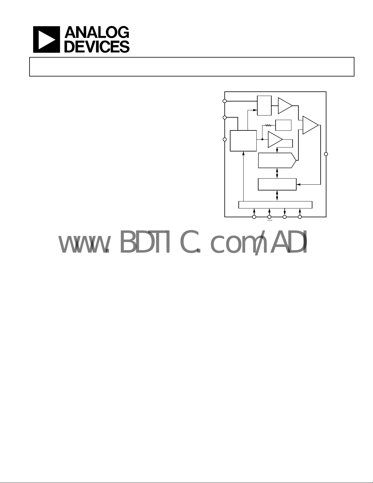
FUNCTIONAL BLOCK DIAGRAM
AIN0
IN1/
V
REF
V
DD
AIN1/V
SOFTWARE
CONTRO L
LATCH
REF
DIN
I/P
MUX
REDISTRIBUTI ON
T/H
2.5V
REF
BUF
CHARGE
DAC
SAR + ADC
CONTRO L LO GIC
SPORT
DOUT
CS
Figure 1.
AD7887
AD7887
COMP
SCLK
GND
6191-001
GENERAL DESCRIPTION
The AD7887 is a high speed, low power, 12-bit analog-to-digital
converter (ADC) that operates from a single 2.7 V to 5.25 V
power supply. The AD7887 is capable of 125 kSPS throughput
rate. The input track-and-hold acquires a signal in 500 ns and
features a single-ended sampling scheme. The output coding for
the AD7887 is straight binary, and the part is capable of
converting full power signals of up to 2.5 MHz.
The AD7887 can be configured for either dual- or single-channel
peration via the on-chip control register. There is a default
o
single-channel mode that allows the AD7887 to be operated as a
read-only ADC. In single-channel operation, there is one
analog input (AIN0) and the AIN1/V
function. This V
pin allows the user access to the part’s
REF
internal 2.5 V reference, or the V
external reference to provide the reference voltage for the part.
This external reference voltage has a range of 2.5 V to V
analog input range on AIN0 is 0 to V
In dual-channel operation, the AIN1/V
function, providing a second analog input channel. In this case,
the reference voltage for the part is provided via the V
pin assumes its V
REF
pin can be overdriven by an
REF
DD
.
REF
pin assumes its AIN1
REF
pin. As
DD
REF
. The
a result, the input voltage range on both the AIN0 and AIN1
inputs is 0 to V
DD
.
CMOS construction ensures low power dissipation of typically
2 mW fo
r normal operation and 3 μW in power-down mode.
The part is available in an 8-lead, 0.15-inch-wide narrow body
SOIC and an 8-lead MSOP package.
PRODUCT HIGHLIGHTS
1. Smallest 12-bit dual-/single-channel ADC; 8-lead MSOP
package.
owest power 12-bit dual-/single-channel ADC.
2. L
lexible power management options, including automatic
3. F
power-down after conversion.
ad-only ADC capability.
4. Re
5. Ana
6. V
log input range from 0 V to V
ersatile serial input/output port (SPI/QSPI/MICROWIRE/
DSP compatible).
REF
.
Rev. C
Information furnished by Analog Devices is believed to be accurate and reliable. However, no
responsibility is assumed by Anal og Devices for its use, nor for any infringements of patents or ot her
rights of third parties that may result from its use. Specifications subject to change without notice. No
license is granted by implication or otherwise under any patent or patent rights of Analog Devices.
Trademarks and registered trademarks are the property of their respective owners.
One Technology Way, P.O. Box 9106, Norwood, MA 02062-9106, U.S.A.
Tel: 781.329.4700 www.analog.com
Fax: 781.461.3113 ©2006 Analog Devices, Inc. All rights reserved.

AD7887
www.BDTIC.com/ADI
TABLE OF CONTENTS
Features.............................................................................................. 1
Applications....................................................................................... 1
Functional Block Diagram .............................................................. 1
General Description ......................................................................... 1
Product Highlights ........................................................................... 1
Revision History ............................................................................... 2
Specifications..................................................................................... 3
Timing Specifications .................................................................. 5
Absolute Maximum Ratings............................................................ 6
ESD Caution.................................................................................. 6
Pin Configurations and Function Descriptions ........................... 7
Typical Performance Characteristics ............................................. 8
Terminology ...................................................................................... 9
Control Register.............................................................................. 10
Theory of Operation ...................................................................... 11
Circuit Information.................................................................... 11
Converter Operation.................................................................. 11
ADC Transfer Function............................................................. 11
Typical Connection Diagram ................................................... 11
Analog Input............................................................................... 12
Power-Down Options................................................................ 13
Power vs. Throughput Rate....................................................... 13
Modes of Operation................................................................... 13
Serial Interface............................................................................ 17
Microprocessor Interfacing....................................................... 18
Application Hints ....................................................................... 20
Outline Dimensions....................................................................... 21
Ordering Guide............................................................................... 21
REVISION HISTORY
9/06—Rev. B to Rev. C
Updated Format..................................................................Universal
Change to Absolute Maximum Ratings......................................... 6
Additions to Pin Configurations.................................................... 7
Added Table 7.................................................................................. 18
Updated Outline Dimensions....................................................... 21
Changes to Ordering Guide.......................................................... 21
Rev. C | Page 2 of 24

AD7887
www.BDTIC.com/ADI
SPECIFICATIONS
VDD = 2.7 V to 5.25 V, V
Table 1.
Parameter
DYNAMIC PERFORMANCE
Signal to Noise + Distortion Ratio (SNR)2, 371 71 dB typ fIN = 10 kHz sine wave, f
Total Harmonic Distortion (THD)2 −80 −80 dB typ fIN = 10 kHz sine wave, f
Peak Harmonic or Spurious Noise2 –80 −80 dB typ fIN = 10 kHz sine wave, f
Intermodulation Distortion (IMD)2
Second-Order Terms −80 −80 dB typ fa = 9.983 kHz, fb = 10.05 kHz, f
Third-Order Terms −80 −80 dB typ fa = 9.983 kHz, fb = 10.05 kHz, f
Channel-to-Channel Isolation2 −80 −80 dB typ fIN = 25 kHz
Full-Power Bandwidth 2.5 2.5 MHz typ @ 3 dB
DC ACCURACY Any channel
Resolution 12 12 Bits
Integral Nonlinearity2 ±2 ±1 LSB max
Differential Nonlinearity2 ±2 ±1 LSB max Guaranteed no missing codes to 11 bits (A Grade)
Offset Error2 ±3 ±3 LSB max VDD = 5 V, dual-channel mode
±4 ±4 LSB max VDD = 3 V, dual-channel mode
±6 ±6 LSB typ Single-channel mode
Offset Error Match2 0.5 0.5 LSB max
Gain Error2 ±2 ±2 LSB max Dual-channel mode
±1 ±1 LSB max Single-channel mode, external reference
±6 ±6 LSB typ Single-channel mode, internal reference
Gain Error Match2 2 2 LSB max
ANALOG INPUT
Input Voltage Ranges 0 to V
Leakage Current ±5 ±5 μA max
Input Capacitance 20 20 pF typ
REFERENCE INPUT/OUTPUT
REFIN Input Voltage Range 2.5/VDD 2.5/VDD V min/max Functional from 1.2 V
Input Impedance 10 10 kΩ typ Very high impedance if internal reference disabled
REF
Output Voltage 2.45/2.55 2.45/2.55 V min/max
OUT
REF
Temperature Coefficient ±50 ±50 ppm/°C typ
OUT
LOGIC INPUTS
Input High Voltage, V
2.1 2.1 V min VDD = 2.7 V to 3.6 V
Input Low Voltage, V
Input Current, IIN ±1 ±1 μA max Typically 10 nA, VIN = 0 V or VDD
Input Capacitance, C
LOGIC OUTPUTS
Output High Voltage, VOH I
V
Output Low Voltage, VOL 0.4 0.4 V max I
Floating-State Leakage Current ±1 ±1 μA max
Floating-State Output Capacitance5 10 10 pF max
Output Coding Straight (Natural) Binary
= 2.5 V, external/internal reference unless otherwise noted, f
REF
A
V
2.4 2.4 V min VDD = 4.75 V to 5.25 V
INH
0.8 0.8 V max VDD = 2.7 V to 5.25 V
INL
4
IN
10 10 pF max
1
ersion
REF
− 0.5 VDD − 0.5 V min VDD = 2.7 V to 5.25 V
DD
B Version1Unit Test Conditions/Comments
0 to V
V
REF
= 2 MHz, TA = T
SCLK
SOURCE
= 200 μA
SINK
MIN
= 200 μA
to T
, unless otherwise noted.
MAX
= 125 kSPS
SAMPLE
= 125 kSPS
SAMPLE
= 125 kSPS
SAMPLE
SAMPLE
SAMPLE
= 125 kSPS
= 125 kSPS
Rev. C | Page 3 of 24

AD7887
www.BDTIC.com/ADI
A
Parameter
Version
CONVERSION RATE
Throughput Time 16 16 SCLK cycles
Track/Hold Acquisition Time2 1.5 1.5 SCLK cycles
Conversion Time 14.5 14.5 SCLK cycles 7.25 μs (2 MHz Clock)
POWER REQUIREMENTS
VDD +2.7/+5.25 +2.7/+5.25 V min/max
IDD
Normal Mode5 (Mode 2)
Static 700 700 μA max
Operational (f
= 125 kSPS) 850 850 μA typ Internal reference enabled
SAMPLE
700 700 μA typ Internal reference disabled
Using Standby Mode (Mode 4) 450 450 μA typ f
Using Shutdown Mode (Modes 1, 3) 120 120 μA typ f
12 12 μA typ f
Standby Mode6 210 210 μA max VDD = 2.7 V to 5.25 V
Shutdown Mode6 1 1 μA max VDD = 2.7 V to 3.6 V
2 2 μA max VDD = 4.75 V to 5.25 V
Normal Mode Power Dissipation 3.5 3.5 mW max VDD = 5 V
2.1 2.1 mW max VDD = 3 V
Shutdown Power Dissipation 5 5 μW max VDD = 5 V
3 3 μW max VDD = 3 V
Standby Power Dissipation 1.05 1.05 mW max VDD = 5 V
630 630 μW max VDD = 3 V
1
Temperature range for A and B versions is −40°C to +125°C.
2
See the Terminology section.
3
SNR calculation includes distortion and noise components.
4
Sample tested at +25°C to ensure compliance.
5
All digital inputs at GND except CS at VDD. No load on the digital outputs. Analog inputs at GND.
6
SCLK at GND when SCLK off. All digital inputs at GND except for CS at VDD. No load on the digital outputs. Analog inputs at GND.
1
B Version1Unit Test Conditions/Comments
Conversion time plus acquisition time is 125 kSPS,
with 2 MH
SAMPLE
SAMPLE
SAMPLE
z Clock
= 50 kSPS
= 10 kSPS
= 1 kSPS
Rev. C | Page 4 of 24

AD7887
O
www.BDTIC.com/ADI
TIMING SPECIFICATIONS
1
Table 2.
Limit at T
MIN
, T
MAX
(A, B Versions)
Parameter 4.75 V to 5.25 V 2.7 V to 3.6 V Unit Description
2
f
2 2 MHz max
SCLK
t
14.5 × t
CONVER T
t
1.5 × t
ACQ
14.5 × t
SCLK
1.5 × t
SCLK
SCLK
SCLK
t1 10 10 ns min
3
t
2
3
t
3
30 60 ns max
75 100 ns max Data access time after SCLK falling edge
Throughput time = t
to SCLK setup time
CS
Delay from CS
until DOUT three-state disabled
CONVER T
+ t
ACQ
= 16 t
SCLK
t4 20 20 ns min Data setup time prior to SCLK rising edge
t5 20 20 ns min Data valid to SCLK hold time
t6 0.4 × t
t7 0.4 × t
4
t
8
80 80 ns max
0.4 × t
SCLK
0.4 × t
SCLK
ns min SCLK high pulse width
SCLK
ns min SCLK low pulse width
SCLK
rising edge to DOUT high impedance
CS
t9 5 5 μs typ Power-up time from shutdown
1
Sample tested at 25°C to ensure compliance. All input signals are specified with tr = tf = 5 ns (10% to 90% of VDD) and timed from a voltage level of 1.6 V.
2
Mark/space ratio for the SCLK input is 40/60 to 60/40.
3
Measured with the load circuit of Figure 2 and defined as the time required for the output to cross 0.8 V or 2.0 V.
4
t8 is derived from the measured time taken by the data outputs to change 0.5 V when loaded with the circuit of Figure 2. The measured number is then extrapolated
back to remove the effects of charging or discharging the 50 pF capacitor. This means that the time, t8, quoted in the timing characteristics is the true bus relinquish
time of the part and is independent of the bus loading.
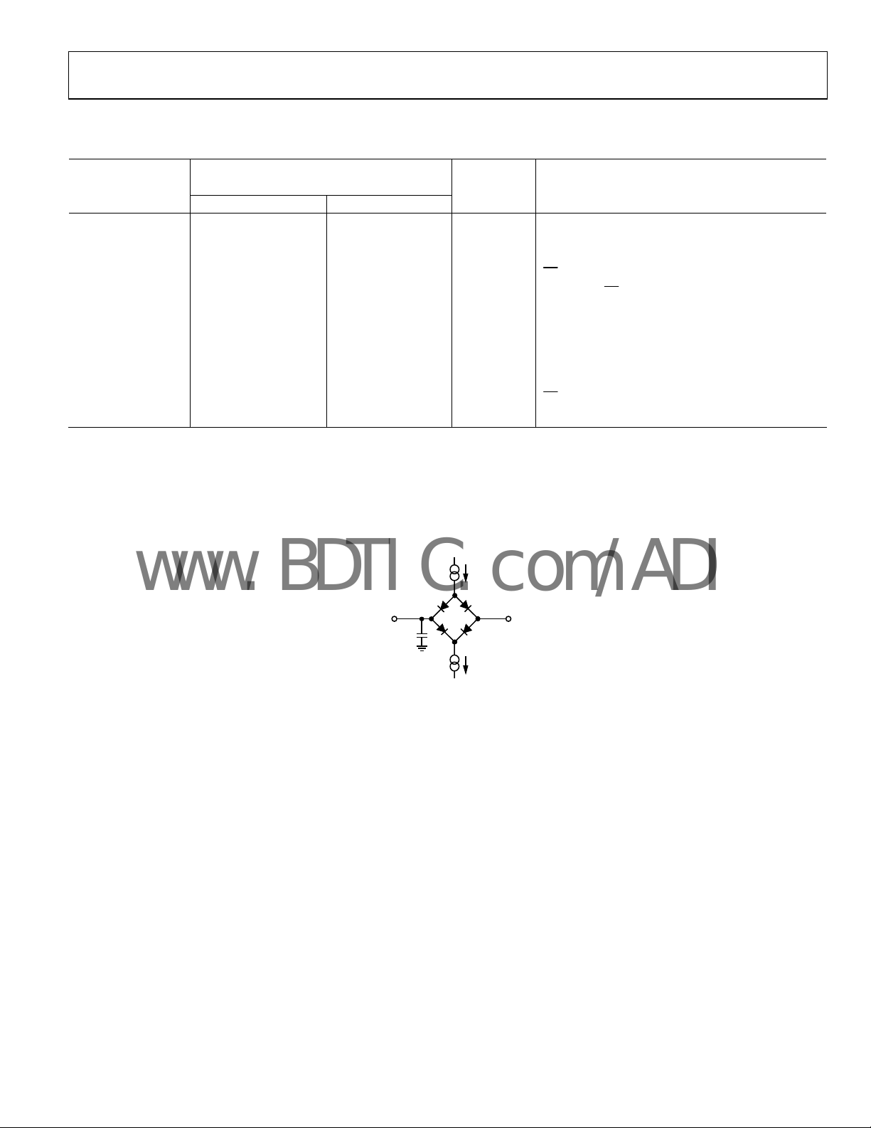
200µA I
TO
UTPUT
PIN
C
L
50pF
200µA I
Figure 2. Load Circuit for Digital Out
OL
1.6V
OH
06191-002
put Timing Specifications
Rev. C | Page 5 of 24

AD7887
www.BDTIC.com/ADI
ABSOLUTE MAXIMUM RATINGS
TA = 25°C, unless otherwise noted.
Table 3.
Parameter Rating
VDD to AGND −0.3 V to +7 V
Analog Input Voltage to AGND −0.3 V to VDD + 0.3 V
Digital Input Voltage to AGND −0.3 V to VDD + 0.3 V
Digital Output Voltage to AGND −0.3 V to VDD + 0.3 V
REFIN/REF
Input Current to Any Pin Except Supplies1 ±10 mA
Operating Temperature Range
Commercial Temperature Range
Storage Temperature Range −65°C to +150°C
Junction Temperature +150°C
SOIC or MSOP Package Power Dissipation 450 mW
θJA Thermal Impedance 157°C/W (SOIC)
205.9°C/W (MSOP)
θJC Thermal Impedance 56°C/W (SOIC)
43.74°C/W (MSOP)
Lead Temperature, Soldering
Pb-Free Temperature, Soldering Reflow 260(0)°C
ESD 4 kV
1
Transient currents of up to 100 mA do not cause SCR latch-up.
to AGND −0.3 V to VDD + 0.3 V
OUT
A, B Versions −40°C to +125°C
Vapor Phase (60 sec) 215°C
Infrared (15 sec) 220°C
Stresses above those listed under Absolute Maximum Ratings
may cause permanent damage to the device. This is a stress
rating only; functional operation of the device at these or any
other conditions above those indicated in the operational
section of this specification is not implied. Exposure to absolute
maximum rating conditions for extended periods may affect
device reliability.
ESD CAUTION
Rev. C | Page 6 of 24

AD7887
www.BDTIC.com/ADI
PIN CONFIGURATIONS AND FUNCTION DESCRIPTIONS
1
CS
AD7887
2
V
DD
GND
3
TOP VIEW
(Not to Scale)
REF
4
AIN1/V
Figure 3. SOIC_N Pin Configuration Figure 4. MSOP Pin Configuration
Table 4. Pin Function Descriptions
Pin No. Mnemonic Description
1
Chip Select. Active low logic input. This input provides the dual function of initiating conversions on the AD7887
CS
and also frames the serial data transfer. When the AD7887 operates in its default mode, the CS
the shutdown pin such that with the CS
2 VDD
Power Supply Input. The V
two-channel operation, this pin also provides the reference source for the part.
3 GND
Ground Pin. This pin is the ground reference point for all cir
and DGND planes, these planes should be tied together as close as possible to this GND pin. Where this is not
possible, this GND pin should connect to the AGND plane.
4 AIN1/V
REF
Analog Input 1/Voltage Reference Input. In single-channel mod
In this case, the user can either access the internal 2.5 V reference or overdrive the internal reference with the
voltage applied to this pin. The reference voltage range for an externally applied reference is 1.2 V to V
channel mode, this pin provides the second analog input channel, AIN1. The input voltage range on AIN1 is
0 to V
.
DD
5 AIN0
Analog Input 0. In single-channel mode, this is the analog input and the input v
channel mode, it has an analog input range of 0 to V
6 DIN
Data In. Logic Input. Data to be written to the AD7887’s contr
the register on the rising edge of SCLK (see the Control Register section). The AD7887 can be operated as a
-channel, read-only ADC by tying the DIN line permanently to GND.
single
7 DOUT
Data Out. Logic output. The conversion result from the AD7887 is provided on this output as a ser
The bits are clocked out on the falling edge of the SCLK input. The data stream consists of four leading zeros
followed by the 12 bits of conversion data, which is provided MSB first.
8 SCLK
Serial Clock. Logic input. SCLK provides the serial clock for ac
the control register. This clock input is also used as the clock source for the AD7887’s conversion process.
8
7
6
5
SCLK
DOUT
DIN
AIN0
1
CS
AD7887
2
V
DD
GND
AIN1/V
06191-003
REF
TOP VIEW
3
(Not to Scale)
4
pin high, the AD7887 is in its power-down mode.
range for the AD7887 is from 2.7 V to 5.25 V. When the AD7887 is configured for
DD
cuitry on the AD7887. In systems with separate AGND
e, this pin becomes the reference input/output.
.
DD
ol register is provided on this input and clocked into
cessing data from the part and writing serial data to
8
SCLK
DOUT
7
DIN
6
AIN0
5
06191-004
pin also acts as
oltage range is 0 to V
ial data stream.
. In two-
DD
. In dual-
REF
Rev. C | Page 7 of 24

AD7887
R
–
www.BDTIC.com/ADI
TYPICAL PERFORMANCE CHARACTERISTICS
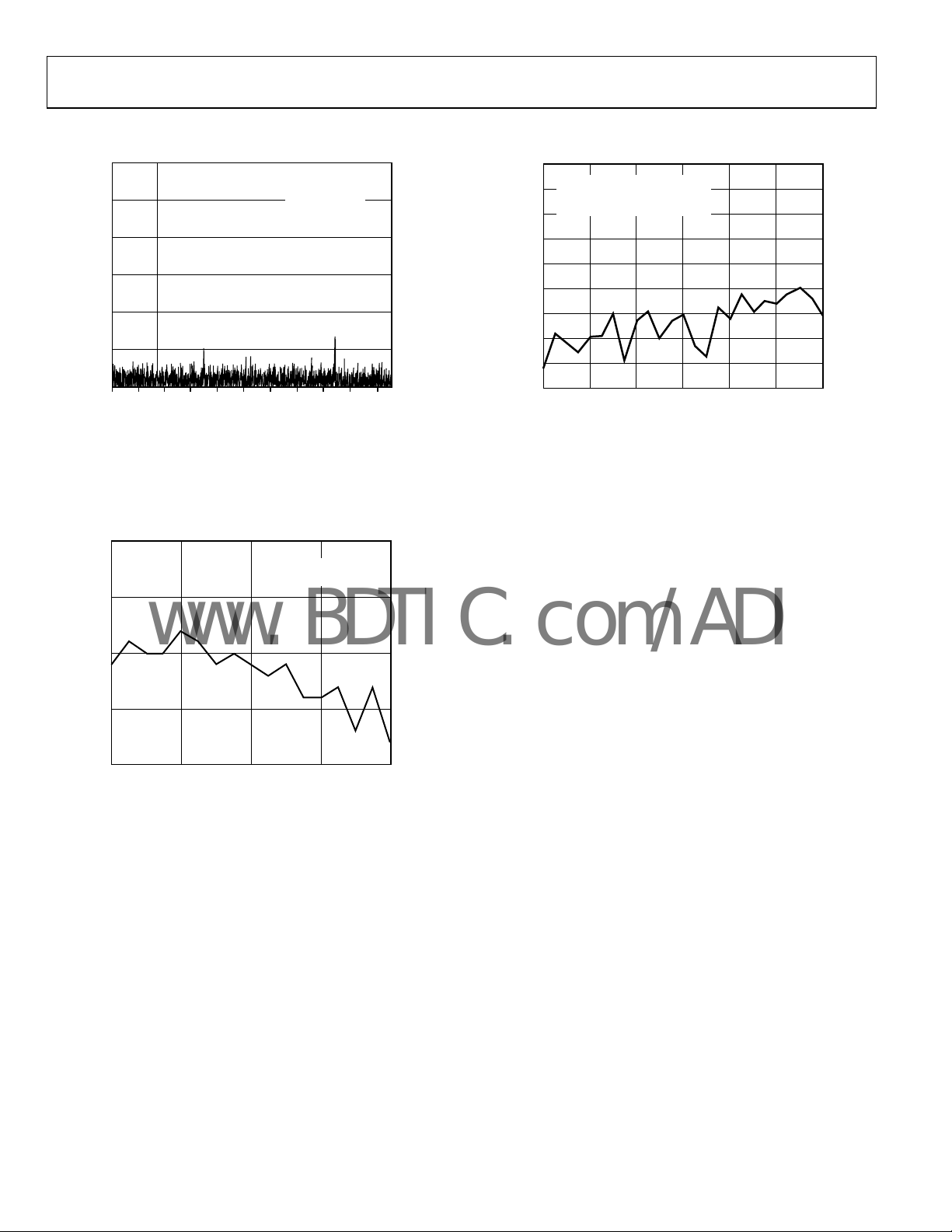
–10
–30
–50
–70
–90
–110
0
4096 POINT FFT
SAMPLING
125kSPS
f
= 10kHz
IN
SNR = 71dB
6.103516012.20703
18.31055
24.41406
30.51758
36.62109
42.72461
48.82813
54.93164
61.03516
06191-005
Figure 5. Dynamic Performance
75
VDD = 5.5V/2. 7V
–77
100mV p-p SI NE WAVE O N V
REFIN = 2.488V EXT REFERENCE
–79
–81
–83
–85
PSRR (dB)
–87
–89
–91
–93
2.65
12.85
Figure 7. PSRR vs. Frequency
DD
23.15 33.65
INPUT FREQ UENCY (kHz)
43.85 54.35
64.15
06191-007
73.0
VDD = 5V
5V EXT REFERENCE
72.5
(dB)
72.0
SN
71.5
71.0
0.15 42.14
21.14
INPUT FREQ UENCY (kHz)
31.5910.89
6191-006
Figure 6. SNR vs. Input Frequency
Rev. C | Page 8 of 24
 Loading...