REV.D
Information furnished by Analog Devices is believed to be accurate and
reliable. However, no responsibility is assumed by Analog Devices for its
use, nor for any infringements of patents or other rights of third parties that
may result from its use. No license is granted by implication or otherwise
under any patent or patent rights of Analog Devices.
a
AD7884/AD7885
One Technology Way, P.O. Box 9106, Norwood, MA 02062-9106, U.S.A.
Tel: 781/329-4700S www.analog.com
Fax: 781/326-8703S © Analog Devices, Inc., 2002
LC2MOS
16-Bit, High-Speed Sampling ADCs
A1
ⴞ5VINF
ⴞ5V
IN
S
AV
SS
VSS
V
REF+FVREF+SVINVVREF–
R4
4k⍀
R7
2k⍀
R8
2k⍀
R6
2k⍀
R5
4k⍀
A2
SW3
R1
5k⍀
R2
3k⍀
ⴞ3V
IN
S
16-BIT
ACCURATE
DAC
LATCH
+
ALU
O
U
T
P
U
T
D
R
I
V
E
R
S
9-BIT
ADC
R3
3k⍀
C1
SW1
SW2
V
REF–
CONVST
V
DD
9
9
9
16
16
DB0
AD7884
TIMER
CONTROL
DGND
CS
RD
BUSY
DB15
AGNDS
AGNDF
AV
DD
GND
ⴞ3VINF
A1
HBEN
ⴞ5VINF
ⴞ5V
IN
S
AV
SS
VSS
V
REF+FVREF+SVINVVREF–
R4
4k⍀
R7
2k⍀
R8
2k⍀
R6
2k⍀
R5
4k⍀
A2
SW3
R1
5k⍀
R2
3k⍀
ⴞ3V
IN
16-BIT
ACCURATE
DAC
LATCH
+
ALU
O
U
T
P
U
T
D
R
I
V
E
R
S
9-BIT
ADC
R3
3k⍀
C1
SW1
SW2
V
REF–
CONVST
V
DD
9
9
9
16
8
DB0
AD7885
TIMER
CONTROL
DGND
CS
RD
BUSY
DB7
AGNDS
AGNDF
AV
DD
GND
FEATURES
Monolithic Construction
Fast Conversion: 5.3 s
High Throughput: 166 kSPS
Low Power: 250 mW
APPLICATIONS
Automatic Test Equipment
Medical Instrumentation
Industrial Control
Data Acquisition Systems
Robotics
GENERAL DESCRIPTION
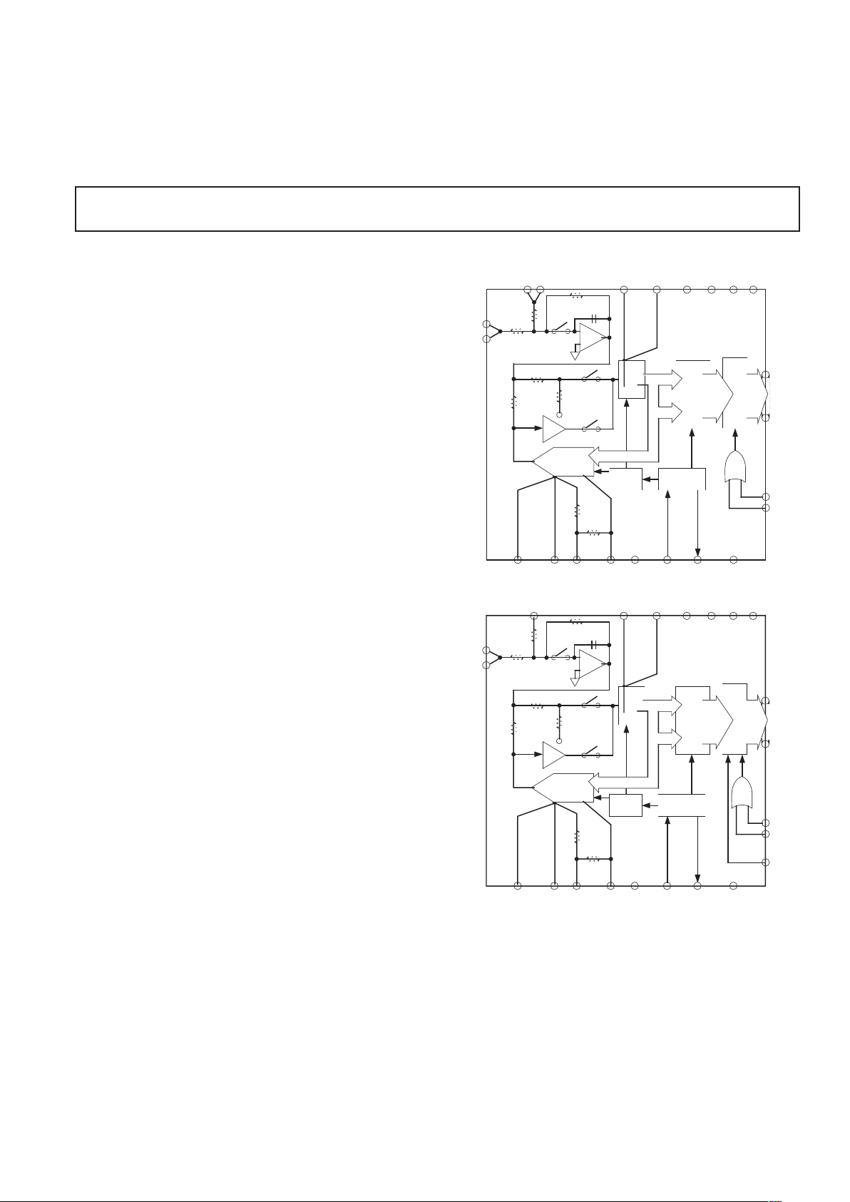
The AD7884/AD7885 is a 16-bit monolithic analog-to-digital
converter with internal sample-and-hold and a conversion time
of 5.3 µs. The maximum throughput rate is 166 kSPS. It uses a
two-pass flash architecture to achieve this speed. Two input
ranges are available: ±5 V and ±3 V. Conversion is initiated by
the CONVST signal. The result can be read into a microprocessor
using the CS and RD inputs on the device. The AD7884 has a
16-bit parallel reading structure while the AD7885 has a byte reading
structure. The conversion result is in two’s complement code.
The AD7884/AD7885 has its own internal oscillator which controls
conversion. It runs from ±5 V supplies and needs a V
REF+
of 3 V.
The AD7884 is available in a 40-lead Cerdip package and in a
44-lead PLCC package.
The AD7885 is available in a 28-lead Cerdip package and the AD7885A
is available in a 44-lead PLCC package.
FUNCTIONAL BLOCK DIAGRAMS

REV. D
–2–
AD7884/AD7885/AD7885A–SPECIFICATIONS
(VDD = 5 V ⴞ 5%, VSS = –5 V ⴞ 5%,
V
REF
+S = 3 V; AGND = DGND = GND = 0 V; f
SAMPLE
= 166 kHz. All specifications T
MIN
to T
MAX
, unless otherwise noted.)
JAB
Parameter Version
1, 2, 3
Version
1, 2, 3
Versions
1, 2, 3
Unit Test Conditions/Comments
DC ACCURACY
Resolution 16 16 16 Bits
Minimum Resolution for Which
No Missing Codes Are Guaranteed 16 16 16 Bits
Integral Nonlinearity ± 0.0075 % FSR max Typically 0.003% FSR
Positive Gain Error ± 0.1 ± 0.03 ± 0.03 % FSR typ AD7885AN/BN: 0.1% typ
Positive Gain Error ± 0.05 % FSR max AD7885BN: 0.2% max
Gain TC
4
± 2 ± 2 ± 2 ppm FSR/°C typ
Bipolar Zero Error ± 0.05 ± 0.05 ± 0.05 % FSR typ
Bipolar Zero Error ± 0.15 % FSR max
Bipolar Zero TC
4
± 8 ± 8 ± 8 ppm FSR/°C typ
Negative Gain Error ± 0.1 ± 0.03 ± 0.03 % FSR typ AD7885AN/BN: 0.1% typ
Negative Gain Error ± 0.05 % FSR max AD7885BN: 0.2% max
Offset TC
4
± 2 ± 2 ± 2 ppm FSR/°C typ
Noise 120 120 120 µV rms typ 78 µV rms typical in ±3 V Input Range
DYNAMIC PERFORMANCE
Signal to (Noise + Distortion) Ratio 82 84 84 dB min Input Signal: ±5 V, 1 kHz Sine Wave, Typically 86 dB
82 82 82 dB typ Input Signal: ± 5 V, 12 kHz Sine Wave
Total Harmonic Distortion –84 –88 –88 dB max Input Signal: ±5 V, 1 kHz Sine Wave
–84 –84 –84 dB typ Input Signal: ±5 V, 12 kHz Sine Wave
Peak Harmonic or Spurious Noise –88 –88 –88 dB max Input Signal: ±5 V, 1 kHz Sine Wave
Intermodulation Distortion (IMD)
Second Order Terms –84 –84 –84 dB typ f
A
= 11.5 kHz, fB = 12 kHz, f
SAMPLE
= 166 kHz
Third Order Terms –84 –84 –84 dB typ fA = 11.5 kHz, fB = 12 kHz, f
SAMPLE
= 166 kHz
CONVERSION TIME
Conversion Time 5.3 5.3 5.3 µs max
Acquisition Time 2.5 2.5 2.5 µs max
Throughput Rate 166 166 166 kSPS max There is an overlap between conversion and acquisition.
ANALOG INPUT
Voltage Range ± 5 ± 5 ± 5 Volts
± 3 ± 3 ± 3 Volts
Input Current ± 4 ± 4 ± 4 mA max
REFERENCE INPUT
Reference Input Current ± 5 ± 5 ± 5 mA max V
REF+
S = 3 V
LOGIC INPUTS
Input High Voltage, V
INH
2.4 2.4 2.4 V min VDD = 5 V ± 5%
Input Low Voltage, V
INL
0.8 0.8 0.8 V max VDD = 5 V ± 5%
Input Current, I
IN
± 10 ± 10 ± 10 µA max Input Level = 0 V to V
DD
Input Capacitance, C
IN
4
10 10 10 pF max
LOGIC OUTPUTS
Output High Voltage, V
OH
4.0 4.0 4.0 V min I
SOURCE
= 40 µA
Output Low Voltage, V
OL
0.4 0.4 0.4 V max I
SINK
= 1.6 mA
DB15–DB0
Floating-State Leakage Current 10 10 10 µA max
Floating-State Output Capacitance415 15 15 pF max
POWER REQUIREMENTS
V
DD
5 5 5 V nom ± 5% for Specified Performance
V
SS
–5 –5 –5 V nom ± 5% for Specified Performance
I
DD
35 35 35 mA max Typically 25 mA
I
SS
30 30 30 mA max Typically 25 mA
Power Supply Rejection Ratio
∆Gain/∆V
DD
86 86 86 dB typ
∆Gain/∆V
SS
86 86 86 dB typ
Power Dissipation 325 325 325 mW max Typically 250
mW
NOTES
1
Temperature ranges are as follows: J, A, B Versions: –40°C to +85°C.
2
VIN = ± 5 V.
3
The AD7885AAP has the same specs as the AD7884AP. The AD7885ABP has the same specs as the AD7884BP.
4
Sample tested to ensure compliance.
Specifications subject to change without notice.

REV. D
AD7884/AD7885
–3–
TIMING CHARACTERISTICS
1, 2
Limit at 25ⴗC Limit at T
MIN
, T
MAX
Parameter (All Versions) (A, B, and J Versions) Unit Conditions/Comments
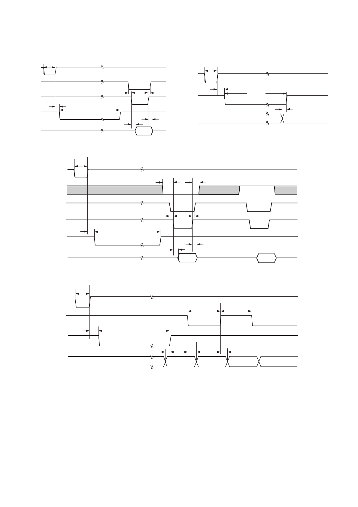
t
1
50 50 ns min CONVST Pulsewidth
t
2
100 100 ns max CONVST to BUSY Low Delay
t
3
0 0 ns min CS to RD Setup Time
t
4
60 60 ns min RD Pulsewidth
t
5
0 0 ns min CS to RD Hold Time
t
6
2
57 57 ns max Data Access Time After RD
t
7
3
5 5 ns min Bus Relinquish Time After RD
50 50 ns max
t
8
40 40 ns min New Data Valid before Rising Edge of BUSY
t
9
10 80 ns min HBEN to RD Setup Time
t
10
25 25 ns min HBEN to RD Hold Time
t
11
60 60 ns min HBEN Low Pulse Duration
t
12
60 60 ns min HBEN High Pulse Duration
t
13
55 70 ns max Propagation Delay from HBEN Falling to Data Valid
t
14
55 70 ns max Propagation Delay from HBEN Rising to Data Valid
NOTES
1
Sample tested at 25°C to ensure compliance. All input signals are specified with tr = tf = 5 ns (10% to 90% of 5 V) and timed from a voltage level of 1.6 V.
2
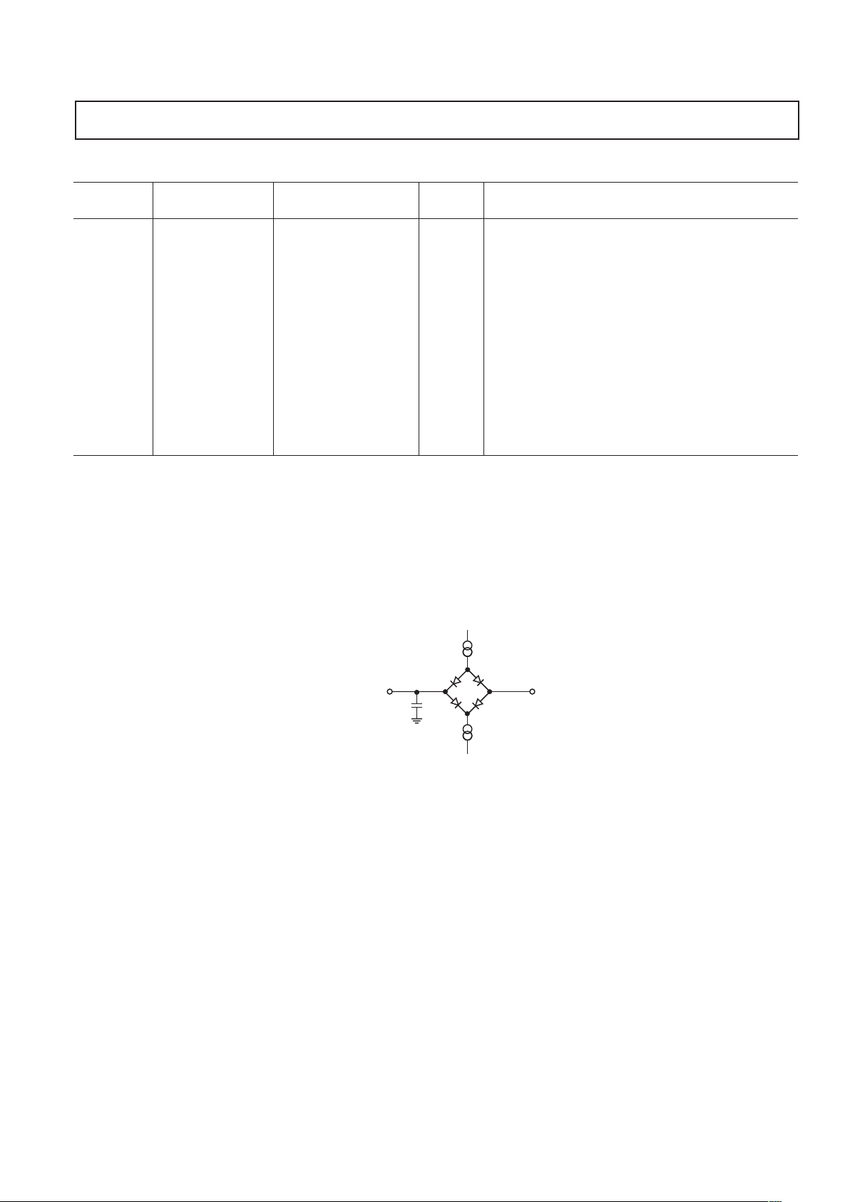
t6 is measured with the load circuit of Figure 1 and defined as the time required for an output to cross 0.8 V or 2.4 V.
3
t7 is derived from the measured time taken by the data outputs to change 0.5 V when loaded with the circuit of Figure 1. The measured number is then
extrapolated back to remove the effects of charging or discharging the 100 pF capacitor. This means that the time, t
7
, quoted in the Timing Characteristics
is the true bus relinquish time of the part and as such is independent of external bus loading capacitances.
Specifications subject to change without notice.
(VDD = +5 V ⴞ 5%, VSS = –5 V ⴞ 5%, AGND = DGND = GND = 0 V. See Figures 2, 3, 4, and 5.)
TO OUTPUT PIN
2.1V
C
L
100pF
200A
IOH
1.6mA
IOL
Figure 1. Load Circuit for Access Time and Bus
Relinquish Time

REV. D
AD7884/AD7885
–4–
t
6
t
2
CS
RD
DATA
BUSY
CONVST
HI-Z
t
3
t
1
t
5
t
7
t
CONVERT
t
4
HI-Z
DATA
VALID
Figure 2. AD7884 Timing Diagram, Using
CS
and
RD
DATA
OLD DATA VALID NEW DATA VALID
BUSY
CONVST
t
1
t
2
t
8
t
CONVERT
Figure 3. AD7884 Timing Diagram, with CS and
RD
Permanently Low
HBEN
CS
RD
DATA
BUSY
CONVST
HI-Z HI-Z
DB0–DB7
DB8–DB15
HI-Z
t
2
DATA
VALID
t
1
DATA
VALID
t
9
t
10
t
3
t
5
t
6
t
7
t
4
t
CONVERT
Figure 4. AD7885 Timing Diagram, Using CS and
RD
DATA
BUSY
HBEN
CONVST
t
1
t
11
t
12
t
2
t
8
t
13
t
14
t
CONVERT
OLD DATA VALID
(DB8–DB15)
NEW DATA VALID
(DB8–DB15)
NEW DATA VALID
(DB0–DB7)
NEW DATA VALID
(DB8–DB15)
NEW DATA VALID
(DB0–DB7)
Figure 5. AD7885 Timing Diagram, with CS and RD Permanently Low

REV. D
AD7884/AD7885
–5–
ORDERING GUIDE
Linearity
Temperature Error SNR Package
Model Range (% FSR) (dB) Option
AD7884AP –40°C to +85°C 84 P-44A
AD7884BP –40°C to +85°C ±0.0075 84 P-44A
AD7885AAP –40°C to +85°C 84 P-44A
AD7885ABP –40°C to +85°C ± 0.0075 84 P-44A
AD7884AQ –40°C to +85°C 84 Q-40
AD7884BQ –40°C to +85°C ±0.0075 84 Q-40
AD7885JQ –40°C to +85°C 82 Q-28
AD7885AQ –40°C to +85°C 84 Q-28
AD7885BQ –40°C to +85°C ±0.0075 84 Q-28
NOTE
P = Plastic Leaded Chip Carrier (PLCC); Q = Cerdip.
ABSOLUTE MAXIMUM RATINGS
1
VDD to AGND . . . . . . . . . . . . . . . . . . . . . . . . . –0.3 V to +7 V
AV
DD
to AGND . . . . . . . . . . . . . . . . . . . . . . . –0.3 V to +7 V
V
SS
to AGND . . . . . . . . . . . . . . . . . . . . . . . . . +0.3 V to –7 V
AV
SS
to AGND . . . . . . . . . . . . . . . . . . . . . . . . –0.3 V to –7 V
AGND Pins to DGND . . . . . . . . . . . . –0.3 V to V
DD
+ 0.3 V
AV
DD
to V
DD
2
. . . . . . . . . . . . . . . . . . . . . . . . . –0.3 V to +7 V
AV
SS
to V
SS
2
. . . . . . . . . . . . . . . . . . . . . . . . . . +0.3 V to –7 V
GND to DGND . . . . . . . . . . . . . . . . . –0.3 V to V
DD
+ 0.3 V
V
IN
S, VINF to AGND . . . . . . . . . . VSS – 0.3 V to VDD + 0.3 V
V
REF+
to AGND . . . . . . . . . . . . . . VSS – 0.3 V to VDD + 0.3 V
V
REF–
to AGND . . . . . . . . . . . . . . . VSS – 0.3 V to VDD + 0.3 V
V
INV
to AGND . . . . . . . . . . . . . . . VSS – 0.3 V to VDD + 0.3 V
Digital Inputs to DGND . . . . . . . . . . . –0.3 V to V
DD
+ 0.3 V
Digital Outputs to DGND . . . . . . . . . . –0.3 V to V
DD
+ 0.3 V
Operating Temperature Range
Commercial Plastic (A, B Versions) . . . . . –40°C to +85°C
Industrial Cerdip (J, A, B Versions) . . . . . . –40°C to +85°C
Storage Temperature Range . . . . . . . . . . . . –65°C to +150°C
Lead Temperature (Soldering, 10 sec) . . . . . . . . . . . . . 300°C
28-Lead Cerdip
θ
JA
Thermal Impedance . . . . . . . . . . . . . . . . . . . . 50.9°C/W
θ
JC
Thermal Impedance . . . . . . . . . . . . . . . . . . . . . 8.3°C/W
40-Lead Cerdip
θ
JA
Thermal Impedance . . . . . . . . . . . . . . . . . . . . 44.5°C/W
44-Lead PLCC
θ
JA
Thermal Impedance . . . . . . . . . . . . . . . . . . . . 47.7°C/W
θ
JC
Thermal Impedance . . . . . . . . . . . . . . . . . . . . 17.5°C/W
Power Dissipation (Any Package) to 75°C . . . . . . . . 1000 mW
Degradation above 75°C by . . . . . . . . . . . . . . . . . . 10 mW/° C
NOTES
1
Stresses above those listed under Absolute Maximum Ratings may cause perma-
nent damage to the device. This is a stress rating only; functional operation of the
device at these or any other conditions above those listed in the operational
sections of this specification is not implied. Exposure to absolute maximum rating
conditions for extended periods may affect device reliability.
2
If the AD7884/AD7885 is being powered from separate analog and digital supplies,
AVSS should always come up before VSS. See Figure 12 for a recommended
protection circuit using Schottky diodes.
CAUTION
ESD (electrostatic discharge) sensitive device. Electrostatic charges as high as 4000 V readily
accumulate on the human body and test equipment and can discharge without detection. Although
the AD7884/AD7885 features proprietary ESD protection circuitry, permanent damage may occur
on devices subjected to high-energy electrostatic discharges. Therefore, proper ESD precautions
are recommended to avoid performance degradation or loss of functionality.
WARNING!
ESD SENSITIVE DEVICE
 Loading...