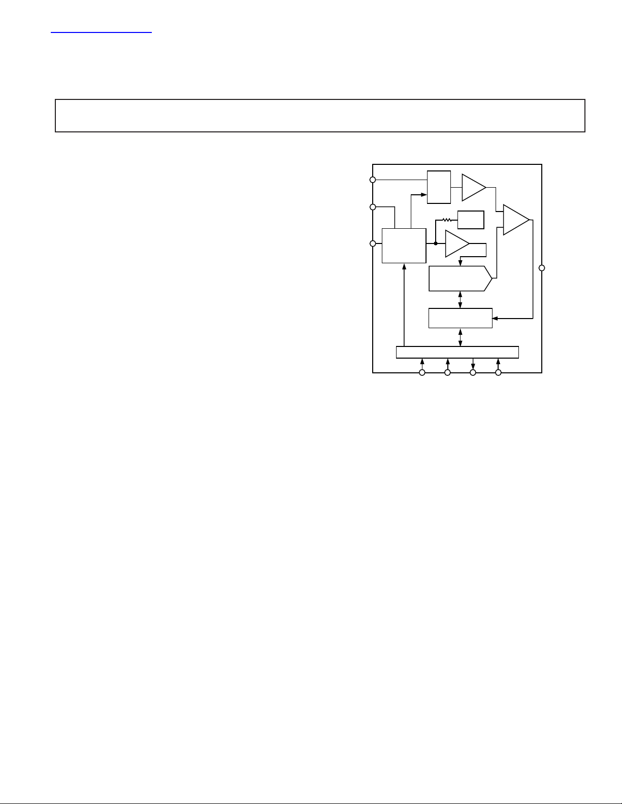
SAR + ADC
CONTROL LOGIC
GND
AIN0
SCLK
DOUT
DIN
V
DD
AD7887
CS
T/H
I/P
MUX
BUF
CHARGE
REDISTRIBUTION
DAC
COMP
V
REF
/AIN1
SOFTWARE
CONTROL
LATCH
V
REF
/
AIN1
2.5V
REF
SPORT
查询AD7887供应商
+2.7 V to +5.25 V, Micropower, 2-Channel,
a
125 kSPS, 12-Bit ADC in 8-Lead mSOIC
FEATURES
Specified for V
of +2.7 V to +5.25 V
DD
Flexible Power/Throughput Rate Management
Shutdown Mode: 1 mA Max
One/Two Single-Ended Inputs
Serial Interface: SPI™/QSPI™/MICROWIRE™/DSP
Compatible
8-Lead Narrow SOIC and mSOIC Packages
APPLICATIONS
Battery-Powered Systems (Personal Digital Assistants,
Medical Instruments, Mobile Communications)
Instrumentation and Control Systems
High Speed Modems
GENERAL DESCRIPTION
The AD7887 is a high speed, low power, 12-bit ADC that operates from a single +2.7 V to +5.25 V power supply. The AD7887
is capable of 125 kSPS throughput rate. The input track-andhold acquires a signal in 500 ns and features a single-ended
sampling scheme. The output coding for the AD7887 is straight
binary and the part is capable of converting full power signals up to
2.5 MHz.
The AD7887 can be configured for either dual or single chan-
nel operation, via the on-chip Control Register. There is a
default single-channel mode that allows the AD7887 to be
operated as a read-only ADC. In single-channel operation,
there is one analog input (AIN0) with the V
suming its V
function. This V
REF
pin allows the user access
REF
to the part’s internal +2.5 V reference, or the V
/AIN1 pin as-
REF
pin can be
REF
overdriven by an external reference to provide the reference
voltage for the part. This external reference voltage has a range
of +2.5 V to V
In dual-channel operation, the V
. The analog input range on AIN0 is 0 to +V
DD
/AIN1 pin assumes its AIN1
REF
function, providing a second analog input channel. In this case,
the reference voltage for the part is provided via the V
pin. As
DD
a result, the input voltage range on both the AIN0 and AIN1
inputs is 0 to V
SPI and QSPI are trademarks of Motorola, Inc.
MICROWIRE is a trademark of National Semiconductor Corporation.
DD
.
REV. B
Information furnished by Analog Devices is believed to be accurate and
reliable. However, no responsibility is assumed by Analog Devices for its
use, nor for any infringements of patents or other rights of third parties
which may result from its use. No license is granted by implication or
otherwise under any patent or patent rights of Analog Devices.
REF
AD7887
FUNCTIONAL BLOCK DIAGRAM
CMOS construction ensures low power dissipation of typically
2 mW for normal operation and 3 µW in power-down mode.
The part is available in an 8-lead, 0.15-inch-wide narrow body
SOIC and an 8-lead µSOIC package.
PRODUCT HIGHLIGHTS
1. Smallest 12-bit dual/single-channel ADC; 8-lead µSOIC
package.
2. Lowest power 12-bit dual/single-channel ADC.
3. Flexible power management options including automatic
.
power-down after conversion.
4. Read-Only ADC capability.
5. Analog input range from 0 V to V
REF
.
6. Versatile serial I/O port (SPI/QSPI/MICROWIRE/DSP
compatible).
One Technology Way, P.O. Box 9106, Norwood, MA 02062-9106, U.S.A.
Tel: 781/329-4700 World Wide Web Site: http://www.analog.com
Fax: 781/326-8703 © Analog Devices, Inc., 1999

AD7887–SPECIFICA TIONS
(VDD = +2.7 V to +5.25 V, V
1
noted, f
= 2 MHz; TA = T
SCLK
= +2.5 V External/Internal Reference unless otherwise
REF
to T
MIN
, unless otherwise noted.)
MAX
Parameter A Version1B Version1Units Test Conditions/Comments
DYNAMIC PERFORMANCE
Signal to Noise + Distortion
2, 3
Ratio
(SNR) 71 71 dB t yp fIN = 10 kHz Sine Wave, f
Total Harmonic Distortion
Peak Harmonic or Spurious Noise
Intermodulation Distortion
2
(THD) –80 –80 dB typ f
2
2
(IMD)
–80 –80 dB typ fIN = 10 kHz Sine Wave, f
= 10 kHz Sine Wave, f
IN
Second Order Terms –80 –80 dB typ fa = 9.983 kHz, fb = 10.05 kHz, f
Third Order Terms –80 –80 dB typ fa = 9.983 kHz, fb = 10.05 kHz, f
Channel-to-Channel Isolation
2
–80 –80 dB typ fIN = 25 kHz
SAMPLE
SAMPLE
SAMPLE
= 125 kSPS
= 125 kSPS
= 125 kSPS
= 125 kSPS
SAMPLE
= 125 kSPS
SAMPLE
Full Power Bandwidth 2.5 2.5 MHz typ @ 3 dB
DC ACCURACY Any Channel
Resolution 12 12 Bits
Integral Nonlinearity
Differential Nonlinearity
Offset Error
Offset Error Match
Gain Error
2
2
2
2
±2 ±1 LSB max
±2 ±1 LSB max Guaranteed No Missing Codes to 11 Bits (A Grade)
±3 ±3 LSB max VDD = 5 V, Dual-Channel Mode
±4 ±4 LSB max V
2
±6 ±6 LSB typ Single-Channel Mode
0.5 0.5 LSB max
= 3 V, Dual-Channel Mode
DD
±2 ±2 LSB max Dual-Channel Mode
±1 ±1 LSB max Single-Channel Mode, External Reference
±6 ±6 LSB typ Single-Channel Mode, Internal Reference
2 2 LSB max
Gain Error Match
2
ANALOG INPUT
Input Voltage Ranges 0 to V
REF
0 to V
REF
Volts
Leakage Current ±5 ±5 µA max
Input Capacitance 20 20 pF typ
REFERENCE INPUT/OUTPUT
REFIN Input Voltage Range 2.5/V
DD
2.5/V
DD
V min/max Functional from 1.2 V
Input Impedance 10 10 kΩ typ Very High Impedance If Internal Reference Disabled
REF
REF
Output Voltage 2.45/2.55 2.45/2.55 V min/max
OUT
Tempco ±50 ± 50 ppm/°C typ
OUT
LOGIC INPUTS
Input High Voltage, V
Input Low Voltage, V
Input Current, I
Input Capacitance, C
INL
IN
IN
INH
4
2.4 2.4 V min VDD = +4.75 V to +5.25 V
2.1 2.1 V min V
= +2.7 V to +3.6 V
DD
0.8 0.8 V max VDD = +2.7 V to +5.25 V
±1 ±1 µA max Typically 10 nA, V
= 0 V or V
IN
10 10 pF max
DD
LOGIC OUTPUTS
Output High Voltage, V
Output Low Voltage, V
OL
OH
– 0.5 VDD – 0.5 V min VDD = +2.7 V to +5.25 V
V
DD
0.4 0.4 V max I
I
SOURCE
SINK
= 200 µA
= 200 µA
Floating-State Leakage Current ±1 ±1 µA max
Floating-State Output Capacitance510 10 pF max
Output Coding Straight (Natural) Binary
CONVERSION RATE
Throughput Time 16 16 SCLK Cycles Conversion Time + Acquisition Time 125 kSPS
Track/Hold Acquisition Time
2
1.5 1.5 SCLK Cycles
with 2 MHz Clock
Conversion Time 14.5 14.5 SCLK Cycles 7.25 µs (2 MHz Clock)
–2–
REV. B

Parameter A Version1B Version1Units Test Conditions/Comments
POWER REQUIREMENTS
V
DD
I
DD
+2.7/+5.25 +2.7/+5.25 V min/max
Normal Mode5 (Mode 2)
Static 700 700 µA max
Operational (f
= 125 kSPS) 850 850 µA typ Internal Reference Enabled
SAMPLE
700 700 µA typ Internal Reference Disabled
Using Standby Mode (Mode 4) 450 450 µA typ f
Using Shutdown Mode (Modes 1, 3) 120 120 µA typ f
Standby Mode
6
Shutdown Mode
6
12 12 µA typ f
210 210 µA max V
11µA max V
22µA max V
Normal Mode Power Dissipation 3.5 3.5 mW max V
2.1 2.1 mW max V
Shutdown Power Dissipation 5 5 µW max V
33µW max V
Standby Power Dissipation 1.05 1.05 mW max V
= 50 kSPS
SAMPLE
= 10 kSPS
SAMPLE
= 1 kSPS
SAMPLE
= +2.7 V to +5.25 V
DD
= +2.7 V to +3.6 V
DD
= +4.75 V to +5.25 V
DD
= +5 V
DD
= +3 V
DD
= +5 V
DD
= +3 V
DD
= +5 V
DD
630 630 µW max VDD = +3 V
NOTES
1
Temperature ranges as follows: A, B Versions: –40°C to +125 °C.
2
See Terminology.
3
SNR calculation includes distortion and noise components.
4
Sample tested @ +25°C to ensure compliance.
5
All digital inputs @ GND except CS @ VDD. No load on the digital outputs. Analog inputs @ GND.
6
SCLK @ GND when SCLK off. All digital inputs @ GND except for CS @ VDD. No load on the digital outputs. Analog inputs @ GND.
Specifications subject to change without notice.
AD7887
ABSOLUTE MAXIMUM RATINGS
(TA = +25°C unless otherwise noted)
1
VDD to AGND . . . . . . . . . . . . . . . . . . . . . . . . . –0.3 V to +7 V
Analog Input Voltage to AGND . . . . . –0.3 V to V
Digital Input Voltage to AGND . . . . . . –0.3 V to V
Digital Output Voltage to AGND . . . . –0.3 V to V
REF
/REF
IN
Input Current to Any Pin Except Supplies
to AGND . . . . . . . . . . –0.3 V to VDD + 0.3 V
OUT
2
. . . . . . . ±10 mA
+ 0.3 V
DD
+ 0.3 V
DD
+ 0.3 V
DD
Operating Temperature Range
Commercial
A, B Versions . . . . . . . . . . . . . . . . . . . . –40°C to +125°C
Storage Temperature Range . . . . . . . . . . . –65°C to +150°C
Junction Temperature . . . . . . . . . . . . . . . . . . . . . . . . . +150°C
SOIC, µSOIC Package, Power Dissipation . . . . . . . . 450 mW
θ
Thermal Impedance . . . . . . . . . . . . . . 157°C/W (SOIC)
JA
. . . . . . . . . . . . . . . . . . . . . . . . . . . . . 205.9°C/W (µSOIC)
θ
Thermal Impedance . . . . . . . . . . . . . . . 56°C/W (SOIC)
JC
. . . . . . . . . . . . . . . . . . . . . . . . . . . . . 43.74°C/W (µSOIC)
Lead Temperature, Soldering
Vapor Phase (60 sec) . . . . . . . . . . . . . . . . . . . . . . +215°C
Infrared (15 sec) . . . . . . . . . . . . . . . . . . . . . . . . . . +220°C
ESD . . . . . . . . . . . . . . . . . . . . . . . . . . . . . . . . . . . . . . . . 4.5 kV
NOTES
1
Stresses above those listed under Absolute Maximum Ratings may cause perma-
nent damage to the device. This is a stress rating only; functional operation of the
device at these or any other conditions above those listed in the operational
sections of this specification is not implied. Exposure to absolute maximum rating
conditions for extended periods may affect device reliability.
2
Transient currents of up to 100 mA will not cause SCR latch-up.
ORDERING GUIDE
Model Linearity Error (LSB)
1
Package Options
2
Branding
AD7887AR ±2 SO-8 AD7887AR
AD7887ARM ±2 RM-8 C5A
AD7887BR ±1 SO-8 AD7887BR
EVAL-AD7887CB
EVAL-CONTROL BOARD
NOTES
1
Linearity error here refers to integral linearity error.
2
SO = SOIC; RM = µSOIC.
3
This can be used as a stand-alone evaluation board or in conjunction with the EVAL-CONTROL BOARD for evaluation/demonstration purposes.
4
This board is a complete unit allowing a PC to control and communicate with all Analog Devices evaluation boards ending in the CB designators.
3
4
Evaluation Board
Controller Board
REV. B
–3–

AD7887
TIMING SPECIFICATIONS
Limit at T
1
MIN
, T
MAX
(A, B Versions)
Parameter +4.75 V to +5.25 V +2.7 V to +3.6 V Units Description
2
f
SCLK
t
CONVERT
t
ACQ
t
1
3
t
2
3
t
3
t
4
t
5
t
6
t
7
4
t
8
t
9
NOTES
1
Sample tested at +25°C to ensure compliance. All input signals are specified with tr = tf = 5 ns (10% to 90% of VDD) and timed from a voltage level of 1.6 volts.
2
Mark/Space ratio for the SCLK input is 40/60 to 60/40.
3
Measured with the load circuit of Figure 1 and defined as the time required for the output to cross 0.8 V or 2.0 V.
4
t8 is derived from the measured time taken by the data outputs to change 0.5 V when loaded with the circuit of Figure 1. The measured number is then extrapolated back
to remove the effects of charging or discharging the 50 pF capacitor. This means that the time, t8, quoted in the timing characteristics is the true bus relinquish time of
the part and is independent of the bus loading.
Specifications subject to change without notice.
2 2 MHz max
14.5 t
1.5 t
SCLK
SCLK
14.5 t
1.5 t
SCLK
SCLK
Throughput Time = t
CONVERT
+ t
ACQ
= 16 t
SCLK
10 10 ns min CS to SCLK Setup Time
30 60 ns max Delay from CS Until DOUT Three-State Disabled
75 100 ns max Data Access Time after SCLK Falling Edge
20 20 ns min Data Setup Time Prior to SCLK Rising Edge
20 20 ns min Data Valid to SCLK Hold Time
0.4 t
0.4 t
SCLK
SCLK
0.4 t
0.4 t
SCLK
SCLK
ns min SCLK High Pulsewidth
ns min SCLK Low Pulsewidth
80 80 ns max CS Rising Edge to DOUT High Impedance
55µs typ Power-Up Time from Shutdown
I
OL
+1.6V
I
OH
OUTPUT
PIN
TO
50pF
200mA
C
L
200mA
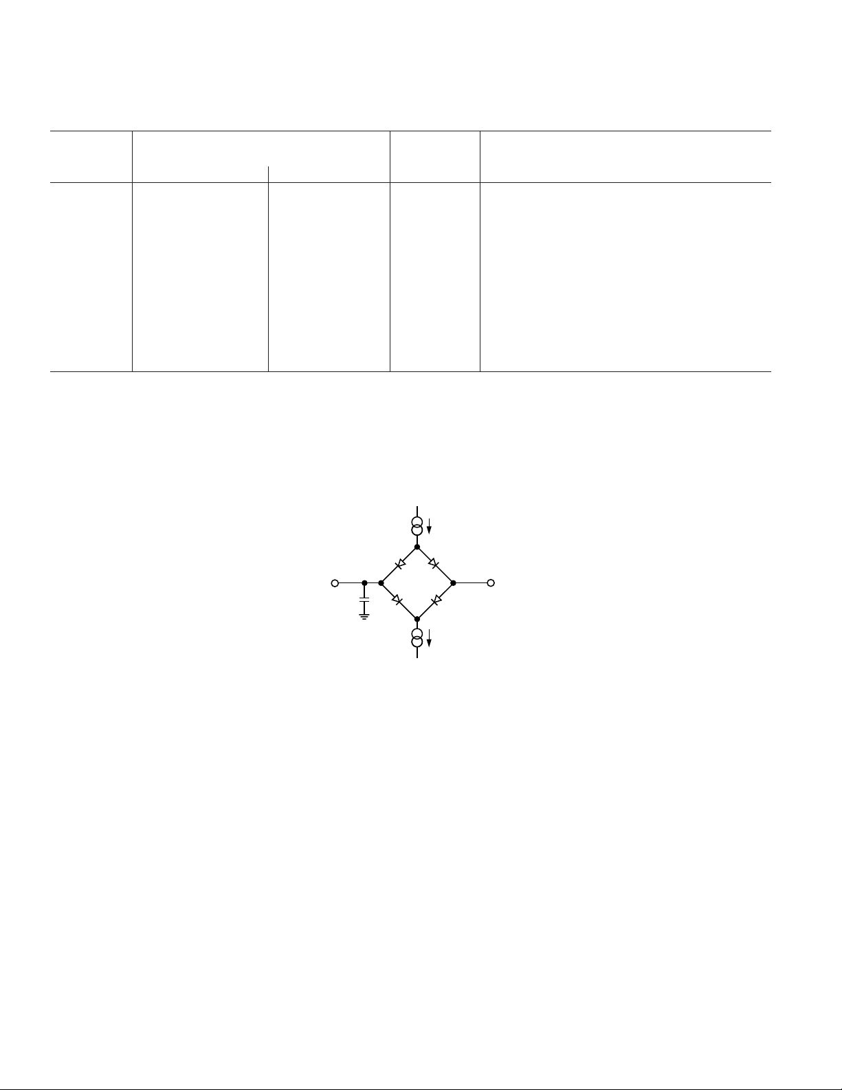
Figure 1. Load Circuit for Digital Output Timing Specifications
–4–
REV. B

PIN CONFIGURATION
AD7887
8
7
6
5
SCLK
DOUT
DIN
AIN0
AIN1/V
CS
V
GND
REF
DD
1
2
AD7887
TOP VIEW
3
(Not to Scale)
4
PIN FUNCTION DESCRIPTIONS
Pin Pin
No. Mnemonic Function
1 CS Chip Select. Active low logic input. This input provides the dual function of initiating conversions on the
AD7887 and also frames the serial data transfer. When the AD7887 operates in its default mode, the CS pin
also acts as the shutdown pin such that with the CS pin high, the AD7887 is in its power-down mode.
2V
DD
Power Supply Input. The VDD range for the AD7887 is from +2.7 V to +5.25 V. When the AD7887 is configured for two-channel operation, this pin also provides the reference source for the part.
3 GND Ground Pin. This pin is the ground reference point for all circuitry on the AD7887. In systems with separate
AGND and DGND planes, these planes should be tied together as close as possible to this GND pin. Where
this is not possible, this GND pin should connect to the AGND plane.
4 AIN1/V
Analog Input 1/Voltage Reference Input. In single-channel mode, this pin becomes the reference input/
REF
output. In this case, the user can either access the internal +2.5 V reference or overdrive the internal reference with the voltage applied to this pin. The reference voltage range for an externally-applied reference is
+1.2 V to V
voltage range on AIN1 is 0 to V
5 AIN0 Analog Input 0. In single-channel mode, this is the analog input and the input voltage range is 0 to V
dual-channel mode, it has an analog input range of 0 to V
. In two-channel mode, this pin provides the second analog input channel AIN1. The input
DD
DD
.
. In
REF
DD
.
6 DIN Data In. Logic Input. Data to be written to the AD7887’s Control Register is provided on this input and is
clocked into the register on the rising edge of SCLK (see Control Register section). The AD7887 can be
operated as a single-channel read-only ADC by tying the DIN line permanently to GND.
7 DOUT Data Out. Logic Output. The conversion result from the AD7887 is provided on this output as a serial data
stream. The bits are clocked out on the falling edge of the SCLK input. The data stream consists of four
leading zeros followed by the 12 bits of conversion data, which is provided MSB first.
8 SCLK Serial Clock. Logic Input. SCLK provides the serial clock for accessing data from the part and writing serial
data to the Control Register. This clock input is also used as the clock source for the AD7887’s conversion
process.
REV. B
–5–
 Loading...