Analog Devices AD7878 a Datasheet
LC2MOS Complete 12-Bit
a
FEATURES
Complete ADC with DSP Interface, Comprising:
Track/Hold Amplifier with 2 ms Acquisition Time
7 ms A/D Converter
3 V Zener Reference
8-Word FIFO and Interface Logic
72 dB SNR at 10 kHz Input Frequency
Interfaces to High Speed DSP Processors, e.g.,
ADSP-2100, TMS32010, TMS32020
41 ns max Data Access Time
Low Power, 60 mW typ
APPLICATIONS
Digital Signal Processing
Speech Recognition and Synthesis
Spectrum Analysis
High Speed Modems
DSP Servo Control
GENERAL DESCRIPTION
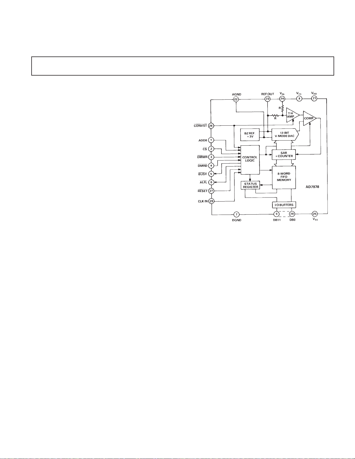
The AD7878 is a fast, complete, 12-bit A/D converter with a
versatile DSP interface consisting of an 8-word, first-in, first-out
(FIFO) memory and associated control logic.
The FIFO memory allows up to eight samples to be digitized
before the microprocessor is required to service the A/D converter. The eight words can then be read out of the FIFO at
maximum microprocessor speed. A fast data access time of
41 ns allows direct interfacing to DSP processors and high
speed 16-bit microprocessors.
An on-chip status/control register allows the user to program the
effective length of the FIFO and contains the FIFO out of
range, FIFO empty and FIFO word count information.
The analog input of the AD7878 has a bipolar range of ± 3 V.
The AD7878 can convert full power signals up to 50 kHz and is
fully specified for dynamic parameters such as signal-to-noise
ratio and harmonic distortion.
The AD7878 is fabricated in Linear Compatible CMOS
2
(LC
MOS), an advanced, mixed technology process that combines precision bipolar circuits with low power CMOS logic.
The part is available in four package styles, 28-pin plastic and
hermetic dual-in-line package (DIP), leadless ceramic chip
carrier (LCCC) or plastic leaded chip carrier (PLCC).
100 kHz Sampling ADC with DSP Interface
AD7878
FUNCTIONAL BLOCK DIAGRAM
PRODUCT HIGHLIGHTS
1. Complete A/D Function with DSP Interface
The AD7878 provides the complete function for digitizing
ac signals to 12-bit accuracy. The part features an on-chip
track/hold, on-chip reference and 12-bit A/D converter. The
additional feature of an 8-word FIFO reduces the high software overheads associated with servicing interrupts in DSP
processors.
2. Dynamic Specifications for DSP Users
The AD7878 is fully specified and tested for ac parameters,
including signal-to-noise ratio, harmonic distortion and
intermodulation distortion. Key digital timing parameters
are also tested and specified over the full operating temperature range.
3. Fast Microprocessor Interface
Data access time of 41 ns is the fastest ever achieved in a
monolithic A/D converter, and makes the AD7878 compatible with all modern 16-bit microprocessors and digital
signal processors.
REV. A
Information furnished by Analog Devices is believed to be accurate and
reliable. However, no responsibility is assumed by Analog Devices for its
use, nor for any infringements of patents or other rights of third parties
which may result from its use. No license is granted by implication or
otherwise under any patent or patent rights of Analog Devices.
One Technology Way, P.O. Box 9106, Norwood, MA 02062-9106, U.S.A.
Tel: 617/329-4700 World Wide Web Site: http://www.analog.com
Fax: 617/326-8703 © Analog Devices, Inc., 1997

AD7878–SPECIFICATIONS
(VDD = +5 V 6 5%, VCC = +5 V 6 5%, VSS = –5 V 6 5%, AGND = DGND =
0 V, f
= 8 MHz. All Specifications T
CLK
MIN
to T
, unless otherwise noted.)
MAX
Parameter Versions1Versions Version Units Test Conditions/Comments
J, A K, L, B S
DYNAMIC PERFORMANCE
Signal-to-Noise Ratio (SNR)3 @ 25°C 70 72 70 dB min VIN = 10 kHz Sine Wave, f
to T
T
MIN
MAX
Total Harmonic Distortion (THD) –80 –80 –78 dB max V
Peak Harmonic or Spurious Noise –80 –80 –78 dB max V
2
= 100 kHz
70 71 70 dB min Typically 71.5 dB for 0 < V
= 10 kHz Sine Wave, f
IN
Typically –86 dB for 0 < V
= 10 kHz, f
IN
SAMPLE
Typically –86 dB for 0 < V
SAMPLE
< 50 kHz
IN
SAMPLE
< 50 kHz
IN
= 100 kHz
< 50 kHz
IN
= 100 kHz
Intermodulation Distortion (IMD)
Second Order Terms –80 –80 –78 dB max fa = 9 kHz, fb = 9.5 kHz, f
Third Order Terms –80 –80 –78 dB max fa = 9 kHz, fb = 9.5 kHz, f
SAMPLE
SAMPLE
= 50 kHz
= 50 kHz
Track/Hold Acquisition Time 2 2 2 µs max See Throughput Rate Section
DC ACCURACY
Resolution 12 12 12 Bits
Minimum Resolution for Which
No Missing Codes are Guaranteed 12 12 12 Bits
Relative Accuracy ±1/2 ±1/4 ±1/2 LSB typ
Differential Nonlinearity ±1/2 ±1/2 ±1/2 LSB typ
Bipolar Zero Error ± 6 ±6 ±6 LSB max
Positive Full-Scale Error
Negative Full-Scale Error
4
4
±6 ±6 ±6 LSB max
±6 ±6 ±6 LSB max
ANALOG INPUT
Input Voltage Range ±3 ±3 ±3 Volts
Input Current ±550 ±550 ±550 µA max
REFERENCE OUTPUT
5
REF OUT 3 3 3 V nom
REF OUT Error @ 25°C ±10 ±10 ±10 mV max
to T
T
MIN
MAX
±15 ±15 ±15 mV max
Reference Load Sensitivity
(∆REF OUT/∆I) ±1 ±1 ±1 mV max Reference Load Current Change (0 µA–500 µA).
Reference Load Should Not Be Changed
During Conversion
LOGIC INPUTS
Input High Voltage, V
Input Low Voltage, V
Input Current, I
Input Capacitance, C
IN
IN
INH
INL
6
+2.4 +2.4 +2.4 V min VCC = +5 V ± 5%
+0.8 +0.8 +0.8 V max VCC = +5 V ± 5%
±10 ±10 ±10 µA max VIN = 0 to V
CC
10 10 10 pF max
LOGIC OUTPUTS
Output High Voltage, V
Output Low Voltage, V
OL
OH
+2.7 +2.7 +2.7 V min I
+0.4 +0.4 +0.4 V max I
SOURCE
= 1.6 mA
SINK
40 µA
DB11–DB0
Floating State Leakage Current ±10 ±10 ±10 ±10 µA max
Floating State Output Capacitance615 15 15 15 pF max
CONVERSION TIME
7/7.125 7/7.125 7/7.125 µs min/µs max Assuming No External Read/Write Operations
7/9.250 7/9.250 7/9.250 µs min/µs max Assuming 17 External Read/Write Operations
See Internal Comparator Timing Section
POWER REQUIREMENTS
V
DD
V
CC
V
SS
I
DD
I
CC
I
SS
+5 +5 +5 V nom ±5% for Specified Performance
+5 +5 +5 V nom ±5% for Specified Performance
–5 –5 –5 V nom ±5% for Specified Performance
13 13 13 mA max CS = DMWR = DMRD = 5 V
100 100 100 µA max CS = DMWR = DMRD = 5 V
6 6 6 mA max CS = DMWR = DMRD = 5 V
Power Dissipation 95.5 95.5 95.5 mW max Typically 60 mW
NOTES
1
Temperature range as follows: J, K, L versions: 0°C to +70°C; A, B versions: –25°C to +85°C; S version: –55°C to +125°C.
2
VIN = ±3 V. See Dynamic Specifications section.
3
SNR calculation includes distortion and noise components.
4
Measured with respect to the Internal Reference.
5
For capacitive loads greater than 50 pF a series resistor is required (see Internal Reference section).
6
Sample tested @ +25°C to ensure compliance.
Specifications subject to change without notice.
–2–
REV. A
1
WARNING!
ESD SENSITIVE DEVICE
TIMING CHARACTERISTICS
Limit at T
MIN
, T
MAX
Limit at T
(VDD = 5 V 6 5%, VCC = 5 V 6 5%, VSS = –5 V 6 5%)
MIN
, T
MAX
Limit at T
MIN
, T
MAX
Parameter (L Grade) (J, K, A, B Grades) (S Grade) Units Conditions/Comments
AD7878
t
l
t
2
t
3
t
4
t
5
t
6
t
7
t
8
2
t
9
3
t
10
t
11
t
12
t
13
2
t
14
t
RESET
NOTES
1
Timing Specifications in bold print are 100% production tested. All other times are sample tested at +25 °C to ensure compliance. All input signals are specified with
tr = tf = 5 ns (10% to 90% of 5 V) and timed from a voltage level of 1.6 V.
2
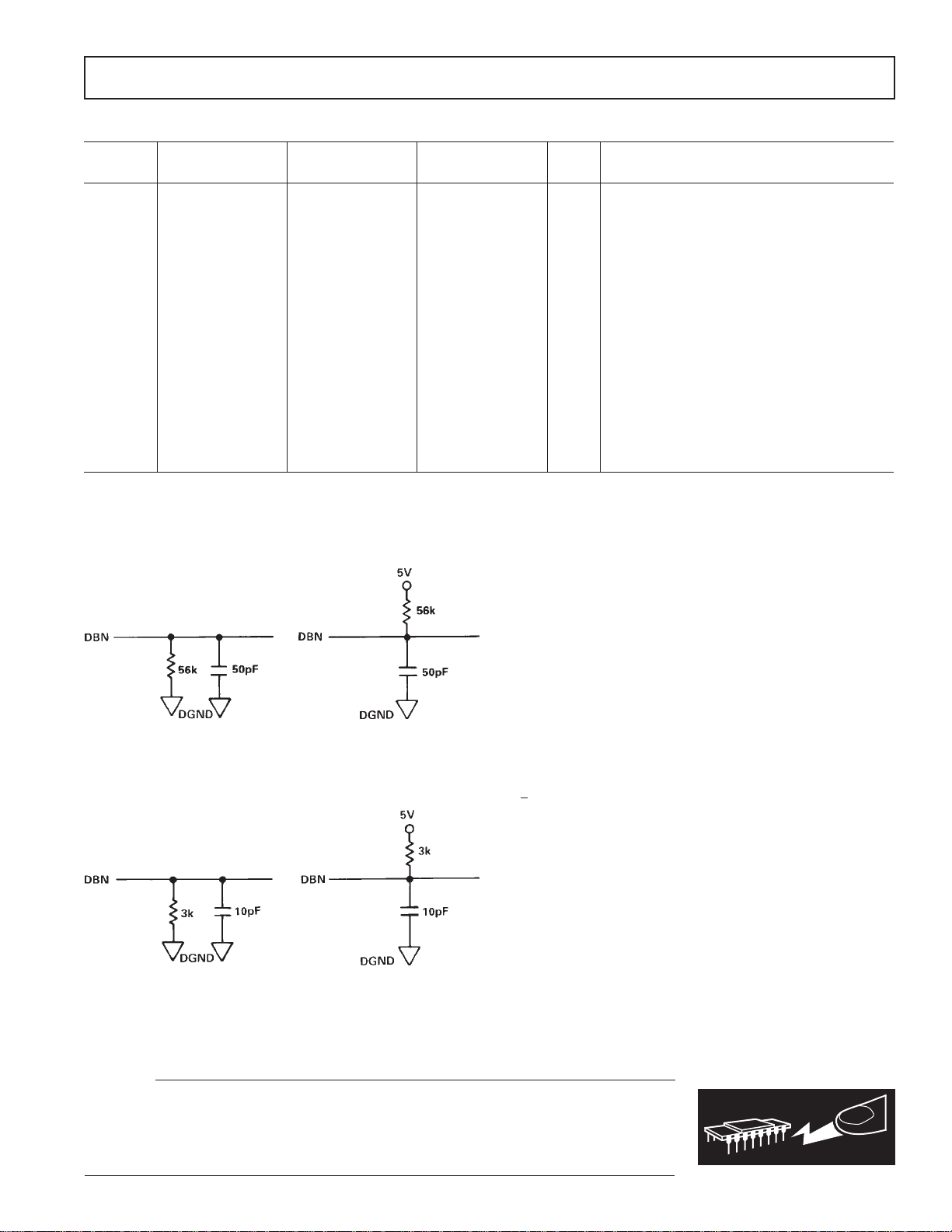
t9 and t14 are measured with the load circuits of Figure 1 and defined as the time required for an output to cross 0.8 V or 2.4 V.
3
t10 is defined as the time required for the data lines to change 0.5 V when loaded with the circuits of Figure 2.
Specifications subject to change without notice.
CAUTION
ESD (electrostatic discharge) sensitive device. Electrostatic charges as high as 4000 V readily
accumulate on the human body and test equipment and can discharge without detection.
Although the AD7878 features proprietary ESD protection circuitry, permanent damage may
occur on devices subjected to high energy electrostatic discharges. Therefore, proper ESD
precautions are recommended to avoid performance degradation or loss of functionality.
REV. A
65 65 75 ns max CLK IN to BUSY Low Propagation Delay
65 65 75 ns max CLK IN to BUSY High Propagation Delay
2 CLK IN Cycles 2 CLK IN Cycles 2 CLK IN Cycles min CONVST Pulse Width
0 0 0 ns min CS to DMRD/REGISTER ENABLE Setup Time
0 0 0 ns min CS to DMRD/ REGISTER ENABLE Hold Time
45 60 60 ns min DMRD Pulse Width
50 50 50 µs max
16 16 16 ns min ADD0 to DMRD/REGISTER ENABLE Setup Time
0 0 0 ns min ADD0 to DMRD/REGISTER ENABLE Hold Time
41 57 57 ns min Data Access Time after DMRD
5 5 5 ns min Bus Relinquish Time
45 45 45 ns max
42 42 55 ns min REGISTER ENABLE Pulse Width
50 50 50 µs max
20 20 30 ns min Data Valid to REGISTER ENABLE Setup Time
10 10 10 ns min Data Hold Time after REGISTER ENABLE
41 57 57 ns min Data Access Time after BUSY
2 CLK IN Cycles 2 CLK IN Cycles 2 CLK IN Cycles min RESET Pulse Width
ABSOLUTE MAXIMUM RATINGS*
(TA = +25°C unless otherwise stated)
VDD to DGND . . . . . . . . . . . . . . . . . . . . . . . . . –0.3 V to +7 V
V
to DGND . . . . . . . . . . . . . . . . . . . . . . . . . –0.3 V to +7 V
CC
V
to DGND . . . . . . . . . . . . . . . . . . . . . . . . . +0.3 V to –7 V
SS
V
to VCC . . . . . . . . . . . . . . . . . . . . . . . . . .–0.3 V to +0.3 V
DD
AGND to DGND . . . . . . . . . . . . . . . . . –0.3 V to V
V
to AGND . . . . . . . . . . . . . . . . . . . . . . . . .–15 V to +15 V
IN
REF OUT to AGND . . . . . . . . . . . . . . . . . . . . . . . . . 0 to V
a. High-Z to V
OH
Figure 1. Load Circuits for Access Time
b. High-Z to V
OL
Digital Inputs to DGND
CLK IN, DMWR, DMRD, RESET,
CS, CONVST, ADD0 . . . . . . . . . . . . –0.3 V to V
Di
gital Outputs to DGND
ALFL, BUSY . . . . . . . . . . . . . . . . . . –0.3 V to V
Data Pins
DB11–DB0 . . . . . . . . . . . . . . . . . . . . –0.3 V to V
Operating Temperature Range
J, K, L Versions . . . . . . . . . . . . . . . . . . . . . . . 0°C to +70°C
A, B Versions . . . . . . . . . . . . . . . . . . . . . . . –25°C to +85°C
S Version . . . . . . . . . . . . . . . . . . . . . . . . . –55°C to +125°C
Storage Temperature Range . . . . . . . . . . . . –65°C to +150°C
Lead Temperature (Soldering, 10 sec) . . . . . . . . . . . .+300°C
Power Dissipation (Any Package) to +75°C . . . . . . 1000 mW
a. V
to High-Z
OH
b. VOL to High-Z
Figure 2. Load Circuits for Output Float Delay
Derates above +75°C by . . . . . . . . . . . . . . . . . . 10 mW/°C
*Stresses above those listed under Absolute Maximum Ratings may cause perma-
nent damage to the device. These are stress rating only; functional operation of the
device at these or any other conditions above those indicated in the operational
sections of this specification is not implied. Exposure to absolute maximum rating
conditions for extended periods may affect device reliability
–3–
+0.3 V
DD
+0.3 V
DD
+0.3 V
DD
+0.3 V
DD
DD
AD7878
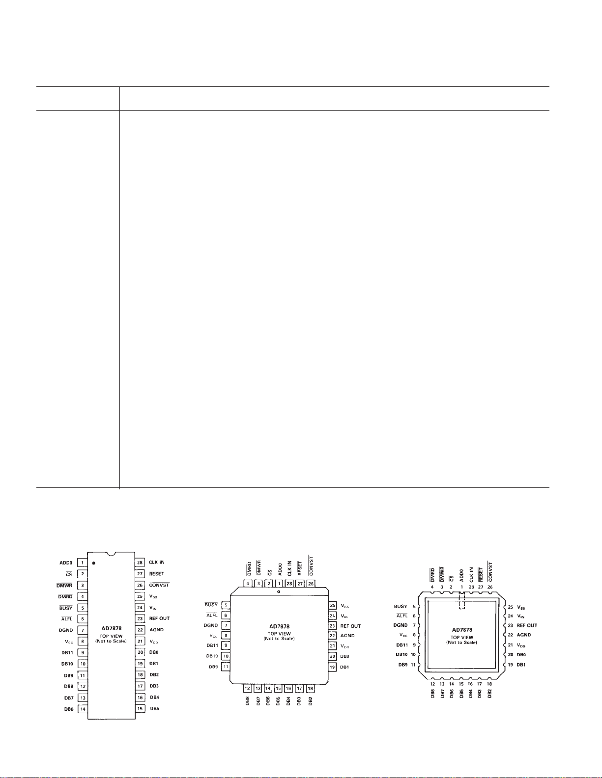
PIN FUNCTION DESCRIPTION
Pin Pin
Number Mnemonic Function
11 ADD0 Address Input. This control input determines whether the word placed on the output data bus during a read operation is a data
word from the FIFO RAM or the contents of the status/control register. A logic low accesses the data word from Location 0 of
the FIFO while a logic high selects the contents of the register (see Status/Control Register section).
12 CS Chip Select. Active low logic input. The device is selected when this input is active.
13 DMWR Dam Memory Write. Active low logic input. DMWR is used in conjunction with CS low and ADD0 high to write data to the
14 DMRD Data Memory READ. Active low logic input. DMRD is used in conjunction with CS low to enable the three-state output buffers.
15 BUSY Active Low Logic Output. This output goes low when the ADC receives a CONVST pulse and remains low until the track/hold
16 ALFL FIFO Almost Full. A logic low indicates that the word count (i.e., number of conversion results) in the FIFO memory has
17 DGND Digital Ground. Ground reference for digital circuitry.
18VCCDigital supply voltage, +5 V ± 5%. Positive supply voltage for digital circuitry.
19 DB11 Data Bit 11 (MSB). Three-state TTL output. Coding for the data words in FIFO RAM is twos complement.
10–15 DB10–DB5 Data Bit 10 to Data Bit 5. Three-state TTL input/outputs.
16–19 DB4–DB1 Data Bit 4 to Data Bit 1. Three-state TTL outputs.
20 DB0 Data Bit 0 (LSB). Three-state TTL output.
21 V
22 AGND Analog Ground. Ground reference for track/hold, reference and DAC.
23 REF OUT Voltage Reference Output. The internal 3 V analog reference is provided at this pin. The external load capability of the reference
24 V
25 V
26 CONVST Convert Start. Logic input. A low to high transition on this input puts the track/hold into its hold mode and starts conversion.
27 RESET Reset. Active low logic input. A logic low sets the words in FIFO memory to 1000 0000 0000 and resets the ALFL output and
28 CLK IN Clock Input. TTL-compatible logic input. Used as the clock source for the A/D converter. The mark-space ratio of this clock can
DD
IN
SS
status/control register. Corresponds to DMWR (ADSP-2100), R/W (MC68000, TMS32020), WE (TMS32010).
Corresponds directly to DMRD (ADSP-2100), DEN (TMS32010).
has gone into its hold mode. The three-state drivers of the AD7878 can be disabled while the BUSY signal is low (see Extended
READ/WRITE section). This is achieved by writing a logic 0 to DB5 (DISO) of the status/control register. Writing a logic 1 to
DB5 of the status/control register allows data to be accessed from the AD7878 while BUSY is low.
reached the programmed word count in the status/control register. ALFL is updated at the end of each conversion. The ALFL
output is reset to a logic high when a word is read from the FIFO memory and the word count is less than the preprogrammed
word count. It can also be set high by writing a logic 1 to DB7 (ENAF) of the status/control register.
Analog positive supply voltage, +5 V ± 5%.
is 500 µA.
Analog Input. Analog input range is ± 3 V.
Analog negative supply voltage, –5 V ± 5%.
The CONVST input is asynchronous to CLK IN and independent of CS, DMWR and DMRD.
status/control register.
vary from 35/65 to 65/35.
DIP
PIN CONFIGURATIONS
PLCC
–4–
LCCC
REV. A

AD7878
ORDERING GUIDE
1, 2
Model
AD7878JN 0°C to +70°C 70 dB 57 ns N-28
AD7878AQ –25°C to +85°C 70 dB 57 ns Q-28
AD7878SQ –55°C to +125°C 70 dB 57 ns Q-28
AD7878KN 0°C to +70°C 72 dB 57 ns N-28
AD7878BQ –25°C to +85°C 72 dB 57 ns Q-28
AD7878LN 0°C to +70°C 72 dB 41 ns N-28
AD7878SE
AD7878JP 0°C to +70°C 70 dB 57 ns P-28A
AD7878KP 0°C to +70°C 72 dB 57 ns P-28A
AD7878LP 0°C to +70°C 72 dB 41 ns P-28A
NOTES
1
To order MIL-STD-883, Class B processed parts, add /883B to part number.
Contact our local sales office for military data sheet.
2
Analog Devices reserves the right to ship either ceramic (D-28) packages or
cerdip (Q-28) hermetic packages.
3
E = Leadless Ceramic Chip Carrier; N = Plastic DIP; P = Plastic Leaded Chip
Carrier, Q = Cerdip.
4
Available to /883B processing only.
Temperature to-Noise Access Package
Range Ratio Time Options
4
–55°C to +125°C 70 dB 57 ns E-28A
Signal- Data
3
STATUS/CONTROL REGISTER
The status/control register serves the dual function of providing
control and monitoring the status of the FIFO memory. This
register is directly accessible through the data bus (DB11–DB0)
with a read or write operation while ADD0 is high. A write
operation to the status/control register provides control for the
ALFL output, bus interface and FIFO counter reset. This is
normally done on power-up initialization. The FIFO memory
address pointer is incremented after each conversion and compared with a preprogrammed count in the status/control register. When this preprogrammed count is reached, the ALFL
output is asserted if the ENAF control bit is set to zero. This
ALFL can be used to interrupt the microprocessor after any
predetermined number of conversions (between 1 and 8). The
status of the address pointer along with sample overrange and
ALFL status can be accessed at any time by reading the status/
control register. Note: reading the status/control register does
not cause any internal data movement in the FIFO memory.
Status information for a particular word should be read from the
status register before the data word is read from the FIFO
memory.
STATUS/CONTROL REGISTER FUNCTION
DESCRIPTION
DB11 (ALFL)
Almost Full Flag, Read only. This is the same as Pin 6 (ALFL
output) status. A logic low indicates that the word count in
the FIFO memory has reached the preprogrammed count in bit
locations DB10–DB8. ALFL is updated at the end of conversion.
DB10–DB8 (AFC2–AFC0)
Almost Full Word Count, Read/Write. The count value determines the number of words in the FIFO memory, which will
cause ALFL to be set. When the FIFO word count equals the
programmed count in these three bits, both the ALFL output
and DB11 of the status register are set to a logic low. For example, when a code of 011 is written to these bits, ALFL is set
when Location 0 through Location 3 of the FIFO memory
contains valid data. AFC2 is the most significant bit of the word
count. The count value can be read back if required.
DB7 (ENAF)
Enable Almost Full, Read/Write. Writing a 1 to this bit disables
the ALFL output and status register bit DB11.
DB6 (FOVR/RESET)
FIFO Overrun/RESET, Read/Write. Reading a 1 from this bit
indicates that at least one sample has been discarded because
the FIFO memory is full. When the FIFO is full (i.e., contains
eight words) any further conversion results will be lost. Writing
a 1 to this bit causes a system RESET as per the RESET input
(Pin 27).
DB5 (FOOR/DISO)
FIFO Out of RANGE/Disable Outputs, Read/Write. Reading a
1 from this bit indicates that at least one sample in the FIFO
memory is out of range. Writing a 0 to this bit prevents the data
bus from becoming active while BUSY is low, regardless of the
state of CS and DMRD.
DB4 (FEMP)
FIFO Empty, Read Only. Reading a 1 indicates there are no
samples in the FIFO memory. When the FIFO is empty the
internal ripple-down effects of the FIFO are disabled and further reads will continue to access the last valid data word in
Location 0.
DB3 (SOOR)
Sample out of Range, Read Only. Reading a 1 indicates the next
sample to be read is out of range, i.e., the sample in Location 0
of the FIFO.
DB–DB0 (FCN2–FCN0)
FIFO Word Count, Read Only. The value read from these bits
indicates the number of samples in the FIFO memory. For
example, reading 011 from these bits indicates that Location 0
through Location 3 contains valid data. Note: reading all 0s
indicates there is either one word or no word in the FIFO
memory; in this case the FIFO Empty determines if there is no
word in memory. FCN2 is the most significant bit.
Table I. Status/Control Bit Function Description
BIT LOCATION DB11 DB10 DB9 DB8 DB7 DB6 DB5 DB4 DB3 DB2 DB1 DB0
STATUS INFORMATION (READ) ALFL AFC2 AFC1 AFC0 ENAF FOVR FOOR FEMP SOOR FCN2 FCN1 FCN0
CONTROL FUNCTION (WRITE) X AFC2 AFC1 AFC0 ENAF RESET DISO XXXXX
RESET STATUS 1 0 0 0 0 0 0 1 0 0 0 0
X =DON’T CARE
REV. A
–5–
 Loading...