


A
3
A
2
A
www.BDTIC.com/ADI
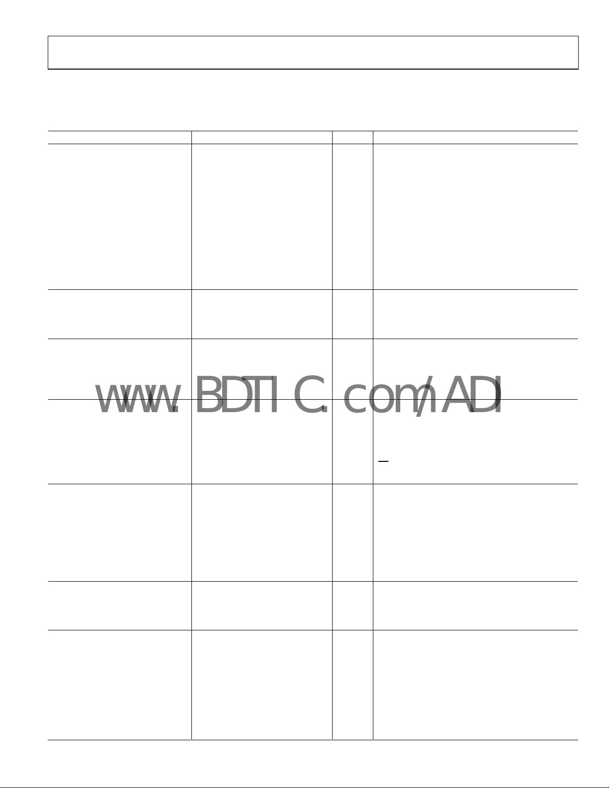
Touch Screen Controller
FEATURES
4-wire touch screen interface
LCD noise reduction feature (STOPACQ pin)
Automatic conversion sequencer and timer
User-programmable conversion parameters
On-chip temperature sensor: −40°C to +85°C
On-chip 2.5 V reference
On-chip 8-bit DAC
3 auxiliary analog inputs
1 dedicated and 3 optional GPIOs
2 direct battery measurement channels (0.5 V to 5 V)
3 interrupt outputs
Touch-pressure measurement
Wake up on touch function
Specified throughput rate of 125 kSPS
Single supply, V
Separate V
Shutdown mode: 1 μA maximum
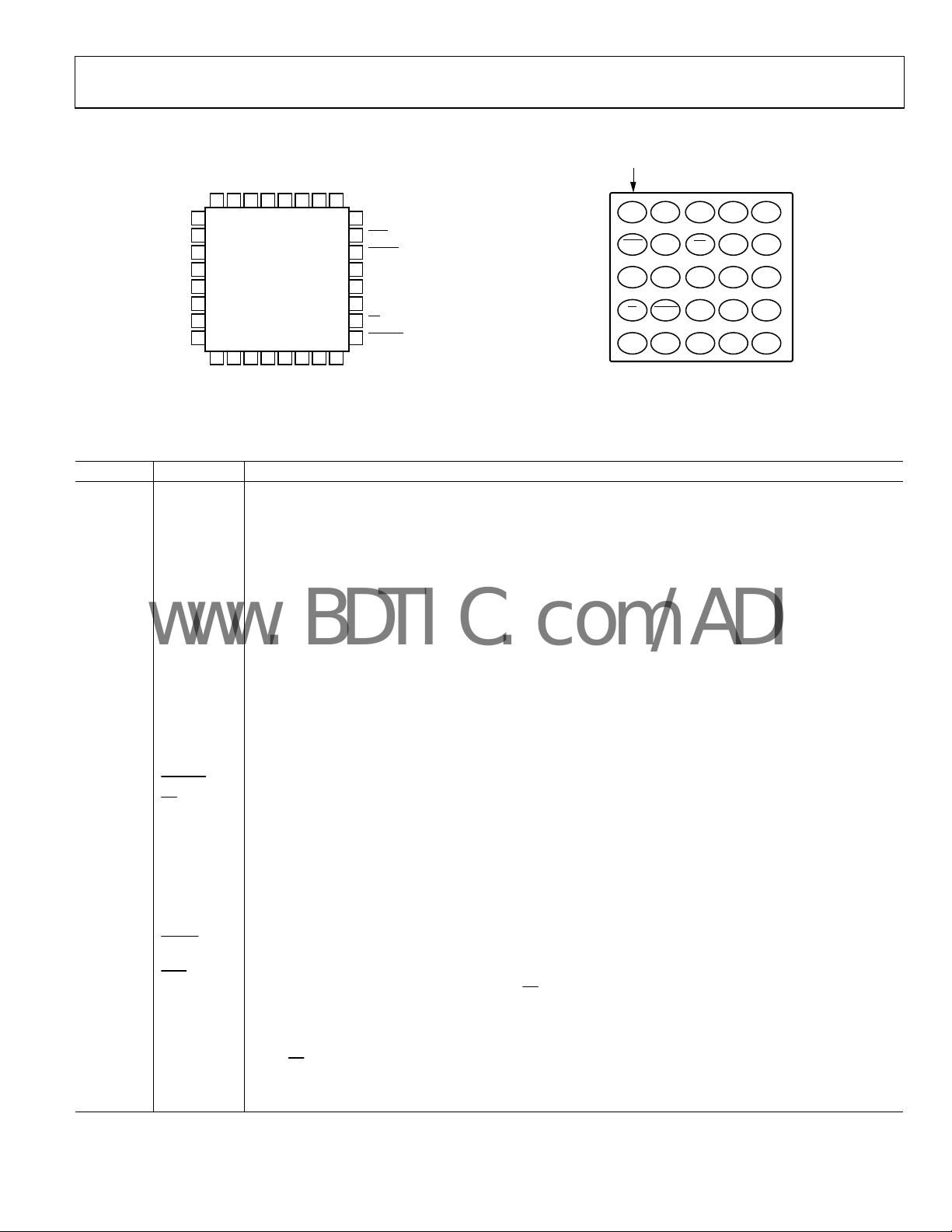
32-lead, LFCSP, 5 mm × 5 mm package
25-ball,WLCSP, 2.5 mm × 2.8 mm package
APPLICATIONS
Personal digital assistants
Smart hand-held devices
Touch screen monitors
Point-of-sale terminals
Medical devices
Cell phones
Pagers
of 2.7 V to 5.25 V
CC
level for serial interface
DRIVE
UX1/GPIO1
UX2/GPIO
UX3/GPIO
BAT1
BAT2
V
AOUT
ARNG
FUNCTIONAL BLOCK DIAGRAM
V
CC
7
12
X+
10
X–
13
Y+
11
Y–
6
5
4
3
BATTERY
MONITOR
2
BATTERY
MONITOR
TEMPERATURE
SENSOR
31
REF
2.5V
REF
30
8-BIT
DAC
29
CONTROL LOGIC AND SERIAL PORT
19
18
DIN26DCLK27DOUT28V
CS23DAV
9 TO 1
BUF
DAC
REGISTER
MUX
I/P
X–
Y– GND X+ Y+ V
12-BIT SUCCESSIVE
APPROXIMATION ADC
WITH TRACK-AND-HOLD
SEQUENCER
REGISTERS
REGISTERS
ALERT STATUS/
MASK REGISTER
REGISTERS
REGISTERS
DRIVE
Figure 1.
RESULTS
CONTROL
DUAL 3-1
MUX
REF–INREF+
COMPARATOR
LIMIT
GPIO
PEN INTERRUPT
AND WAKE-UP
ON TOUCH
AD7877
AD7877
REF
CLOCK
STOP
ACQ
ADC DATA
LOGIC
LIMIT
ALERT
LOGIC
TO
GPIO1-3
20
14
15
22
21
17
STOPACQ
AGND
DGND
ALERT
GPIO4
PENIRQ
03796-001
GENERAL DESCRIPTION
The AD7877 is a 12-bit, successive approximation ADC with a
synchronous serial interface and low on resistance switches for
driving touch screens. The AD7877 operates from a single 2.7 V
to 5.25 V power supply (functional operation to 2.2 V), and
features throughput rates of 125 kSPS. The AD7877 features
direct battery measurement on two inputs, temperature and
touch-pressure measurement.
The AD7877 also has an on-board reference of 2.5 V. When not
e, it can be shut down to conserve power. An external
in us
reference can also be applied and varied from 1 V to +V
an analog input range of 0 V to V
. The device includes a
REF
, with
CC
shutdown mode that reduces its current consumption to less
than 1 μA.
Rev. B
Information furnished by Analog Devices is believed to be accurate and reliable. However, no
responsibility is assumed by Anal og Devices for its use, nor for any infringements of patents or ot her
rights of third parties that may result from its use. Specifications subject to change without notice. No
license is granted by implication or otherwise under any patent or patent rights of Analog Devices.
Trademarks and registered trademarks are the property of their respective owners.
To reduce the effects of noise from LCDs, the acquisition phase
the on-board ADC is controlled via the STOPACQ pin. User-
of
programmable conversion controls include variable acquisition
time and first conversion delay. Up to 16 averages can be taken
per conversion. There is also an on-board DAC for LCD backlight or contrast control. The AD7877 runs in either slave or
master mode using a conversion sequencer and timer. It is ideal
for battery-powered systems such as personal digital assistants
with resistive touch screens and other portable equipment.
The part is available in a 32-lead lead frame chip scale package
P), and a 25-ball wafer level chip scale package (WLCSP).
(LFCS
One Technology Way, P.O. Box 9106, Norwood, MA 02062-9106, U.S.A.
Tel: 781.329.4700 www.analog.com
Fax: 781.461.3113 ©2006 Analog Devices, Inc. All rights reserved.

AD7877
www.BDTIC.com/ADI
TABLE OF CONTENTS
Features.............................................................................................. 1
Control Registers............................................................................ 20
Applications....................................................................................... 1
Functional Block Diagram .............................................................. 1
General Description ......................................................................... 1
Revision History ............................................................................... 2
Specifications..................................................................................... 3
Timing Specifications .................................................................. 5
Timing Diagrams.......................................................................... 5
Absolute Maximum Ratings............................................................ 6
ESD Caution.................................................................................. 6
Pin Configurations and Function Descriptions ........................... 7
Typical Performance Characteristics ............................................. 9
Terminology .................................................................................... 13
Circuit Information........................................................................ 14
Touch Screen Principles ............................................................14
Measuring Touch Screen Inputs............................................... 15
Control Register 1 ...................................................................... 20
Control Register 2 ...................................................................... 21
Sequencer Registers ................................................................... 22
Interrupts..................................................................................... 24
Syncronizing the AD7877 to the Host CPU........................... 25
8-Bit DAC........................................................................................ 26
Serial Interface ................................................................................ 28
Writing Data ............................................................................... 28
Write Timing............................................................................... 29
Reading Data............................................................................... 29
V
Pin..................................................................................... 29
DRIVE
General-Purpose I/O Pins............................................................. 30
GPIO Configuration.................................................................. 30
Grounding and Layout .................................................................. 32
PCB Design Guidelines for Chip Scale Packages................... 32
Touch-Pressure Measurement.................................................. 16
STOPACQ Pin ............................................................................ 16
Temperature Measurement....................................................... 17
Battery Measurement................................................................. 18
Auxiliary Inputs.......................................................................... 19
Limit Comparison...................................................................... 19
REVISION HISTORY
6/06—Changed from Rev. A to Rev. B
Added Wafer Level Chip Scale Package...........................Universal
Changes to Table 3............................................................................ 6
Changes to Figure 21...................................................................... 11
Change to Figure 25 ....................................................................... 12
Changes to Figure 38 and Figure 39............................................. 23
Change to Figure 40 ....................................................................... 24
Changes to Data Available Output (
Updated Outline Dimensions....................................................... 42
Changes to Ordering Guide.......................................................... 42
DAV
) Section ....................24
Register Maps.................................................................................. 33
Detailed Register Descriptions ..................................................... 35
GPIO Registers ........................................................................... 40
Outline Dimensions....................................................................... 42
Ordering Guide .......................................................................... 42
11/04—Changed from Rev. 0 to Rev. A
Changes to Absolute Maximum Ratings .......................................6
C
hanges to Figure 4...........................................................................7
Changes to Table 4.............................................................................7
Changes to Grounding and Layout section ................................ 32
Changes to Figure 42...................................................................... 32
Changes to Ordering Guide.......................................................... 43
7/04—Revision 0: Initial Version
Rev. B | Page 2 of 44
AD7877
www.BDTIC.com/ADI
SPECIFICATIONS
VCC = 2.7 V to 3.6 V, V
Table 1.
Parameter Min Typ Max Unit Test Conditions/Comments
DC ACCURACY
Resolution 12 Bits
No Missing Codes 11 12 Bits
Integral Nonlinearity
Differential Nonlinearity (DNL)1 Minimum LSB size = 610 μV
Negative DNL −0.99 LSB
Positive DNL +2 LSB
Offset Error1 ±2 ±6 LSB VCC = 2.7 V
Gain Error1 ±4 LSB External reference
Noise 70 μV rms
Power Supply Rejection 70 dB
Internal Clock Frequency 2 MHz
SWITCH DRIVERS
On Resistance
Y+, X+ 14 Ω
Y−, X− 14 Ω
ANALOG INPUTS
Input Voltage Ranges 0 V
DC Leakage Current ±0.1 μA
Input Capacitance 30 pF
Accuracy 0.3 % All channels, internal V
REFERENCE INPUT/OUTPUT
Internal Reference Voltage 2.44 2.55 V
Internal Reference Tempco ±50 ppm/°C
V
Input Voltage Range 1 VCC V
REF
DC Leakage Current ±1 μA
V
Input Impedance 1 GΩ
REF
TEMPERATURE MEASUREMENT
Temperature Range −40 +85 °C
Resolution
Differential Method2 1.6 °C
Single Conversion Method3 0.3 °C
Accuracy
Differential Method2 ±4 °C 0°C to 70°C
Single Conversion Method3 ±2 °C Calibrated at 25°C
BATTERY MONITOR
Input Voltage Range 0.5 5 V @ V
Input Impedance 14 kΩ Sampling, 1 GΩ when the battery monitor is off
Accuracy 1 3.2 % External/internal reference, see Figure 26
DAC
Resolution 8 Bits
Integral Nonlinearity ±1 Bits
Differential Nonlinearity ±1 Guaranteed monotonic by design
Voltage Mode
Output Voltage Range 0 − VCC/2 V DAC register Bit 2 = 0, Bit 0 = 0
0 − VCC
Slew Rate −0.4, +0.5 V/μs
Output Settling Time 12 15 μs 0 to 3/4 scale, R
1
= 2.5 V internal or external, f
REF
1
±2 LSB LSB size = 610 μV
= 2 MHz, TA = −40°C to +85°C, unless otherwise noted.
DCLK
V
REF
CS
= GND or VCC; typically 25 Ω when the on-board
reference is enabled
= 2.5 V
REF
Rev. B | Page 3 of 44
V DAC register Bit 2 = 0, Bit 0 = 1
= 10 kΩ, C
LOAD
REF
= 50 pF
LOAD
AD7877
www.BDTIC.com/ADI
Parameter Min Typ Max Unit Test Conditions/Comments
Capacitive Load Stability 50 100 pF R
Output Impedance 75 kΩ Power-down mode
Short-Circuit Current 21 mA
Current Mode
Output Current Range 0 1000 μA DAC register, Bit 2 = 1; full-scale current is set by R
Output Impedance Open Power-down mode
LOGIC INPUTS
Input High Voltage, V
Input Low Voltage, V
0.7 V
INH
INL
V
DRIVE
0.3
V
DRIVE
V
Input Current, IIN ±1 μA Typically 10 nA, VIN = 0 V or V
Input Capacitance, C
4
10 pF
IN
LOGIC OUTPUTS
Output High Voltage, VOH V
− 0.2 V I
DRIVE
Output Low Voltage, VOL 0.4 V I
Floating-State Leakage Current ±10 μA
Floating-State Output Capacitance4 10 pF
Output Coding Straight (natural) binary
CONVERSION RATE
Conversion Time 8 μs
Throughput Rate 125 kSPS
POWER REQUIREMENTS
VCC (Specified Performance) 2.7 3.6 V Functional from 2.2 V to 5.25 V
V
1.65 V
DRIVE
V
CC
ICC Digital I/Ps = 0 V or VCC
Converting Mode 240 380 μA ADC on, internal reference off, V
650 900 μA ADC on, internal reference on, VCC = 3.6 V
900 μA ADC on, internal reference on, DAC on
Static 150 μA
Shutdown Mode 1 μA
1
See the Terminology section.
2
Difference between Temp0 and Temp1 measurement. No calibration necessary.
3
Temperature drift is −2.1 mV/°C.
4
Sample tested @ 25°C to ensure compliance.
= 10 kΩ
LOAD
CC
= 250 μA, VCC/V
SOURCE
= 250 μA
SINK
high to DAV low
CS
ADC on, but not converting, internal reference off,
= 3.6 V
V
CC
= 2.7 V to 5.25 V
DRIVE
CC
= 3.6 V
RNG
Rev. B | Page 4 of 44
AD7877
www.BDTIC.com/ADI
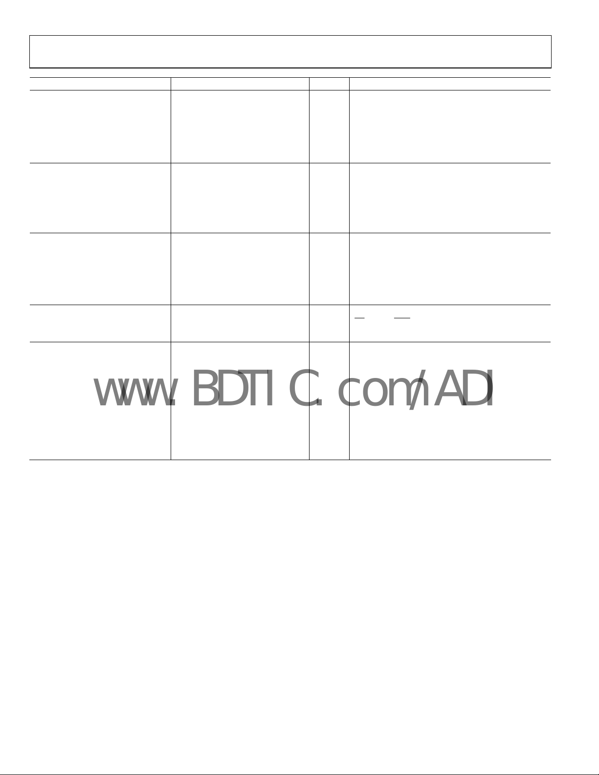
TIMING SPECIFICATIONS
TA = T
signals are specified with t
Table 2.
Parameter Limit at T
f
DCLK
20 MHz max
t
1
t
2
t
20 ns min DCLK low pulse width
3
t
12 ns min DIN setup time
4
t
12 ns min DIN hold time
5
2
t
6
2
t
7
3
t
8
t
0 ns min
9
1
Mark/space ratio for the DCLK input is 40/60 to 60/40.
2
Measured with the load circuit of Figure 3 and defined as the time required for the output to cross 0.4 V or 2.0 V.
3
t8 is derived from the measured time taken by the data outputs to change 0.5 V when loaded with the circuit shown in Figure 3. The measured number is then
extrapolated back to remove the effects of charging or discharging the 50 pF capacitor. This means that the time, t8, quoted in the timing characteristics is the true bus
relinquish time of the part and is independent of the bus loading.
to T
MIN
1
16 ns min
, unless otherwise noted, VCC = 2.7 V to 5.25 V, V
MAX
= tF = 5 ns (10% to 90% of VCC) and timed from a voltage level of 1.6 V.
R
, T
MIN
Unit Description
MAX
10 kHz min
= 2.5 V. Sample tested at 25°C to ensure compliance. All input
REF
falling edge to first DCLK rising edge
CS
20 ns min DCLK high pulse width
16 ns max
falling edge to DOUT, three-state disabled
CS
16 ns max DCLK falling edge to DOUT valid
16 ns max
rising edge to DOUT high impedance
CS
rising edge to DCLK ignored
CS
TIMING DIAGRAMS
CS
t
DCLK
DIN
DOUT
1
1 2 3 15 16
MSB LSB
t
6
MSB LSB
t
2
t
4
Figure 2. Detailed Timing Diagram
TO OUTPUT
PIN
Figure 3. Load Circuit for Digital Out
t
3
t
5
t
7
200μAI
C
L
50pF
200μAI
t
9
t
8
OL
1.6V
OH
03796-003
put Timing Specifications
03796-004
Rev. B | Page 5 of 44
AD7877
www.BDTIC.com/ADI
ABSOLUTE MAXIMUM RATINGS
TA = 25°C, unless otherwise noted.
Table 3.
Parameter Rating
VCC to GND −0.3 V to +7 V
Analog Input Voltage to GND −0.3 V to VCC + 0.3 V
Digital Input Voltage to GND −0.3 V to VCC + 0.3 V
Digital Output Voltage to GND −0.3 V to VCC + 0.3 V
V
to GND −0.3 V to VCC + 0.3 V
REF
Input Current to Any Pin Except Supplies110 mA
ESD Rating (IEC 1000-4-2, Air Discharge)
Tablet Pins (X+, X−, Y+, Y−) 4 kV
Other Pins 2 kV
Operating Temperature Range −40°C to +85°C
Storage Temperature Range −65°C to +150°C
Junction Temperature 150°C
LFCSP Package
Power Dissipation 450 mW
θJA Thermal Impedance 135.7°C/W
IR Reflow Peak Temperature 220°C
Pb-Free Parts Only 260°C (±0.5°C)
Lead Temperature (Soldering 10 sec) 300°C
1
Transient currents of up to 100 mA do not cause SCR latch-up.
Stresses above those listed under Absolute Maximum Ratings
ma
y cause permanent damage to the device. This is a stress
rating only; functional operation of the device at these or any
other conditions above those indicated in the operational
section of this specification is not implied. Exposure to absolute
maximum rating conditions for extended periods may affect
device reliability.
ESD CAUTION
ESD (electrostatic discharge) sensitive device. Electrostatic charges as high as 4000 V readily accumulate on
the human body and test equipment and can discharge without detection. Although this product features
proprietary ESD protection circuitry, permanent damage may occur on devices subjected to high energy
electrostatic discharges. Therefore, proper ESD precautions are recommended to avoid performance
degradation or loss of functionality.
Rev. B | Page 6 of 44
AD7877
A
A
A
E
www.BDTIC.com/ADI
PIN CONFIGURATIONS AND FUNCTION DESCRIPTIONS
PIN 1
REF
NC
V
32 31 30 29 28 27 26 25
1
NC
2
BAT2
3
BAT1
UX3/GPIO3
UX2/GPIO2
UX1/GPIO1
NC = NO CONNECT
4
5
6
7
V
CC
8
NC
9 10 11 12 13 14 15 16
NC
X–
Figure 4. LFCSP Pin Configuration
Table 4. Pin Function Descriptions
Pin No. Mnemonic Description
1, 8, 9, 16,
NC No Connect.
24, 25, 32
2 BAT2 Battery Monitor Input. ADC Input Channel 7.
3 BAT1 Battery Monitor Input. ADC Input Channel 6.
4 AUX3/GPIO3 Auxiliary Analog Input. ADC Input Channel 5. Can be reconfigured as GPIO pin.
5 AUX2/GPIO2 Auxiliary Analog Input. ADC Input Channel 4. Can be reconfigured as GPIO pin.
6 AUX1/GPIO1 Auxiliary Analog Input. ADC Input Channel 3. Can be reconfigured as GPIO pin.
7 V
Power Supply Input. The V
CC
10 X− Touch Screen Position Input.
11 Y− Touch Screen Position Input. ADC Input Channel 2.
12 X+ Touch Screen Position Input. ADC Input Channel 0.
13 Y+ Touch Screen Position Input. ADC Input Channel 1.
14 AGND
15 DGND
17
18
PENIRQ
Chip Select Input. Active low logic input. This input provides the dual function of initiating conversions on the
CS
19 DIN
20 STOPACQ
21 GPIO4 Dedicated General-Purpose Logic Input/Output Pin.
22
23
Digital Active Low Output. Interrupt output that goes low if a GPIO data bit is set, or if the AUX1, TEMP1, BAT1,
ALERT
Data Available Output. Active low logic output. Asserts low when new data is available in the AD7877 results
DAV
26 DCLK External Clock Input. Logic input. DCLK provides the serial clock for accessing data from the part.
27 DOUT
28 V
DRIVE
DRIV
AOUT
ARNG
V
DOUT
DCLK
NC
DCLK
DOUT
V
ARNG
V
REF
BAT1
V
CC
Y–
AOUT
BAT2
AUX3/
GPI03
AUX1/
GPI01
X–
03796-051
24
NC
23
DAV
22
DGND
NC
ALERT
21
GPIO4
20
STOPACQ
19
DIN
18
CS
17
PENIRQ
03796-002
range for the AD7877 is from 2.2 V to 5.25 V.
CC
AD7877
TOP VIEW
(Not to Scale)
Y–
X+
Y+
AGND
Analog Ground. Ground reference point f
DRIVE
ALERT
STOP
ACQ
CS
DGND
DAV
GPIO4
AUX2/
DIN
GPI02
PENIRQ
AGND
Y+
X+
AD7877 WLCSP
TOP VIEW
Not to Scal e
Figure 5. WLCSP Pin Configuration
or all analog circuitry on the AD7877. All analog input signals and any
external reference signal should be referred to this voltage.
Digital Ground. Ground reference for all digital circuitry on the AD7877. Refer all digital input signals to this
ltage.
vo
Pen Interrupt. Digital active low output (has a 50 kΩ in
ternal pull-up resistor).
AD7877 and enabling the serial input/output register.
SPI® Serial Data Input. Data to be written to the AD7877 r
egisters are provided on this input and clocked into
the register on the rising edge of DCLK.
Stop Acquisition Pin. A signal applied to this pin can be monit
ored by the AD7877, so that acquisition of new
data by the ADC is halted while the signal is active. Used to reduce the effect of noise from an LCD screen on
the touch screen measurements.
or BAT2 measurements are out of range.
registers. This output is high impedance when CS
Serial Data Output. Logic output. The conversion result fr
is high.
om the AD7877 is provided on this output as a serial
data stream. The bits are clocked out on the falling edge of the DCLK input. This output is high impedance
when CS
is high.
Logic Power Supply Input. The voltage supplied at this pin determines the operating voltage for the serial
interface of the AD7877.
Rev. B | Page 7 of 44

AD7877
www.BDTIC.com/ADI
Pin No. Mnemonic Description
29 ARNG When the DAC is in current output mode, a resistor from ARNG to GND sets the output range.
30 AOUT Analog Output Voltage or Current from DAC.
31 V
REF
Reference Output for the AD7877. The internal 2.5 V referenc
device. The reference output must be buffered before it is applied elsewhere in a system. To reduce system
noise effects, it is strongly recommended to place a capacitor of 100 nF between the V
Alternatively, an external reference can be applied to this input. The voltage range for the external reference is
1.0 V to VCC. For the specified performance, it is 2.5 V on the AD7877.
e is available on this pin for use external to the
pin and GND.
REF
Rev. B | Page 8 of 44
AD7877
www.BDTIC.com/ADI
TYPICAL PERFORMANCE CHARACTERISTICS
TA = 25°C, VCC = 2.7 V, V
800
= 2.5 V, f
REF
SAMPLE
= 125 kHz, f
DCLK
= 16 × f
= 2 MHz, unless otherwise noted.
SAMPLE
200
ADC, REF, AND DAC
700
ADC AND REF
CURRENT (μA)
600
500
–50 –30 –10 0 30 50 70 90
TEMPERATURE (°C)
Figure 6. Supply Current vs. Temperature
1000
900
800
700
CURRENT (μA)
600
500
400
2.0 2.3 2.6 2.9 3.2 3.5 3.8 4.1 4.4 4.7 5.0
Figure 7. Supply Current vs. V
ADC, REF, AND DAC
ADC AND REF
VCC (V)
CC
03796-030
03796-031
180
160
140
CURRENT (nA)
120
100
80
–50–30–101030507090
Figure 9. Full Power-Down I
0.6
0.5
0.4
0.3
0.2
0.1
0
–0.1
–0.2
DELTA FROM 25°C (LSB)
–0.3
–0.4
–0.5
–0.6
–50–30–101030507090
Figure 10. Change in ADC Offset v
TEMPERATURE (°C)
vs. Temperature
DD
TEMPERATURE (°C)
s. Temperature
03796-032
03796-040
0.6
0.5
0.4
0.3
0.2
0.1
0
–0.1
–0.2
DELTA FROM 25°C (LSB)
–0.3
–0.4
–0.5
–0.6
–50–30–101030507090
TEMPERATURE (°C)
03796-039
1.0
0.8
0.6
0.4
0.2
0
INL (LSB)
–0.2
–0.4
–0.6
–0.8
–1.0
0 500 1000 1500 2000 2500 3000 3500 4000
Figure 8. Change in ADC Gain vs. Temperature
Rev. B | Page 9 of 44
CODE
Figure 11. ACD INL Plot
03796-044
AD7877
www.BDTIC.com/ADI
1.0
0.8
0.6
0.4
0.2
0
–0.2
DNL (LSB)
–0.4
–0.6
–0.8
–1.0
0 500 1000 1500 2000 2500 3000 3500 4000
CODE
Figure 12. ADC DNL Plot
03796-045
16
14
12
10
8
6
4
REFERENCE CURRENT (μA)
2
0
–50 9070503010–10–30
TEMPERATURE (°C)
Figure 15. External Reference Current vs. Temperature
03796-046
22
20
18
16
(Ω)
ON
14
R
12
10
8
2.73.13.53.94.34.75.15.5
X+ TO V
Y+ TO V
CC
VCC (V)
Figure 13. Switch On Resistance vs. V
(X+, Y+: V
22
20
18
16
(Ω)
ON
14
R
12
to Pin; X−, Y−: Pin to GND)
CC
Y+ TO V
CC
CC
X– TO GND
Y– TO GND
X– TO GND
Y– TO GND
CC
2.520
2.515
2.510
2.505
2.500
(V)
REF
2.495
V
2.490
2.485
2.480
03796-048
2.475
–50–30–101030507090
Figure 16. Internal V
2.508
2.506
2.504
(V)
2.502
REF
V
2.500
TEMPERATURE (°C)
vs. Temperature
REF
03796-033
10
X+ TO V
8
–40 –20 0 20 40 60 80
CC
TEMPERATURE ( °C)
Figure 14. Switch On Resistance vs. Temperature
(X+, Y
+: V
to Pin; X−, Y−: Pin to GND)
CC
03796-049
2.498
2.496
2.6 2.9 3.2 3.5 3.8 4.1 4.4 4.7 5.0
Figure 17. Internal V
Rev. B | Page 10 of 44
VCC (V)
REF
vs. V
03796-034
CC
AD7877
www.BDTIC.com/ADI
3145
3135
3125
3115
3105
3095
3085
3075
ADC CODE (Decimal)
3065
3055
3045
–50–30–101030507090
TEMPERATURE (°C)
Figure 18. ADC Code vs. Temperature (2.7 V Supply)
03796-041
6
(V)
REF
2.5
INTERNAL V
0
NO CAP
0.711μs SETTLING TIME
20 40 60 80 100 120–20 0
TURN-ON TIME (μs)
Figure 21. Internal V
100nF CAP
54.64μs SETTLING TIME
vs. Turn-On Time
REF
03796-047
1183
1182
1181
1180
1179
TEMP1 CODE
1178
1177
1176
2.7 2.8 2.9 3.0 3.1 3.2 3.3 3.4 3.5 3.6
Figure 19. Temp1 vs. V
982
981
980
979
978
TEMP0 CODE
977
976
975
2.7 2.8 2.9 3.0 3.1 3.2 3.3 3.4 3.5 3.6
VCC (V)
VCC (V)
CC
03796-042
03796-043
10
–10
–30
–50
–70
–90
–110
INPUT TONE AMPLITUDE (dB)
–130
–150
0 10k 20k 30k
SNR 70.25dB
THD 78.11dB
FREQUENCY
40k
Figure 22. Typical FFT Plot for the Auxiliary Channels of the AD7877
at 9
0 kHz Sample Rate and 10 kHz Input Frequency
3.50
3.25
3.00
2.75
2.50
2.25
2.00
1.75
1.50
1.25
DAC O/P LEVEL (V)
1.00
0.75
0.50
DAC O/P SINK ABILITY
0.25
0
012345678910
SOURCE/SINK CURRENT (mA)
DAC O/P SOURCE ABILITY
03796-035
03796-036
Figure 20. Temp0 vs. V
CC
Figure 23. DAC Source and Si
Rev. B | Page 11 of 44
nk Current Capability
AD7877
www.BDTIC.com/ADI
1
CH1 200mV CH2 100mV M2.00μs CH1 780mV
Figure 24. DAC O/P Settling Time (Zero Scale to Half Scale)
Δ
: 144mV
@: 1.296V
VDD = 3V
TEMPERATURE = 25°C
03796-037
–2 –1 0 1 2
ERROR (%)
Figure 26. Typical Accuracy for Battery Channel (25°C)
03796-050
600
500
400
DAC SINK CURRENT
300
200
DAC SINK CURRENT (µA)
100
0
0 25 50 75 100 125 150 175 200 225 250
NOTE: MAXIMUM DAC SINK CURRENT I S
SET ACCORDING TO THE EQUATION:
I
= VCC /(R
MAX
INPUT CODE (Decimal)
Figure 25. DAC Sink Current vs. Input Code with R
× 6)
RNG
= 1 kΩ
RNG
03796-038
Rev. B | Page 12 of 44

AD7877
www.BDTIC.com/ADI
TERMINOLOGY
Integral Nonlinearity
The maximum deviation from a straight line passing through
the endpoints of the ADC transfer function. The endpoints of
the transfer function are zero scale at 1 LSB below the first code
transition, and full scale at 1 LSB above the last code transition.
Differential Nonlinearity
ference between the measured and the ideal 1 LSB
The dif
change between any two adjacent codes in the ADC.
Offset Error
The devia
(00…001) from the ideal (AGND + 1 LSB).
Gain Error
The devia
(111…111) from the ideal (V
has been adjusted out.
On Resistance
A me
source of the switch drivers.
tion of the first code transition (00…000) to
tion of the last code transition (111…110) to
− 1 LSB) after the offset error
REF
asure of the ohmic resistance between the drain and the
Rev. B | Page 13 of 44
AD7877
www.BDTIC.com/ADI
CIRCUIT INFORMATION
The AD7877 is a complete, 12-bit data acquisition system for
digitizing positional inputs from a touch screen in PDAs and
other devices. In addition, it can monitor two battery voltages,
ambient temperature, and three auxiliary analog voltages, with
high and low limit comparisons on three of the inputs, and has
up to four general-purpose logic I/O pins.
The core of the AD7877 is a high speed, low power, 12-bit
nalog-to-digital converter (ADC) with input multiplexer,
a
on-chip track-and-hold, and on-chip clock. The results of
conversions are stored in 11 results registers, and the results
from one auxiliary input and two battery inputs can be compared with high and low limits stored in limit registers to generate
an out-of-limit
analog switches to switch the X and Y excitation voltages to the
touch screen, a STOPACQ pin to control the ADC acquisition
period, 2.5 V reference, on-chip temperature sensor, and 8-bit
DAC to control LCD contrast. The high speed SPI serial bus
provides control of, and communication with, the device.
Operating from a single supply from 2.2 V to 5 V, the AD7877
ffers throughput rates of up to 125 kHz. The device is available
o
in a 5 mm × 5 mm, 32-lead, lead frame chip scale package
(LFCSP), and in a 2.5 mm × 2.8 mm, wafer level chip scale
package (WLCSP), with a 5 × 5 ball grid array.
The data acquisition system of the AD7877 has a number of
vanced features:
ad
nput channel sequenced automatically or selected by
• I
the host.
TOPACQ feature to reduce noise from LCD.
• S
veraging of from 1 to 16 conversions for noise reduction.
• A
• Pr
ogrammable acquisition time.
• Po
wer management.
• Pr
ogrammable ADC power-up delay before first
conversion.
hoice of internal or external reference.
• C
• C
onversion at preprogrammed intervals.
TOUCH SCREEN PRINCIPLES
A 4-wire touch screen consists of two flexible, transparent,
resistive-coated layers that are normally separated by a small air
gap. The X layer has conductive electrodes running down the
left and right edges, allowing the application of an excitation
voltage across the X layer from left to right.
ALERT
. The AD7877 also contains low resistance
PLASTIC FILM WITH
TRANSPARENT, RESISTIVE
CONDUCTIVE ELECTRODE
ON BOTTOM SIDE
CONDUCTIVE ELECTRODE
ON TOP SIDE
Figure 27. Basic Construction of a Touch Screen
Y+
LCD SCREEN
COATING ON BOTTOM SIDE
Y–
X+
PLASTIC FILM WITH
TRANSPARENT, RESISTIVE
COATING ON TOP SIDE
X–
The Y layer has conductive electrodes running along the top
and bottom edges, allowing the application of an excitation
voltage down the Y layer from top to bottom.
Provided that the layers are of uniform resistivity, the voltage at
a
ny point between the two electrodes is proportional to the
horizontal position for the X layer and the vertical position for
the Y layer.
When the screen is touched, the two layers make contact. If
o
nly the X layer is excited, the voltage at the point of contact,
and therefore the horizontal position, can be sensed at one of
the Y layer electrodes. Similarly, if only the Y layer is excited,
the voltage, and therefore the vertical position, can be sensed at
one of the X layer electrodes. By switching alternately between
X and Y excitation and measuring the voltages, the X and
Y coordinates of the contact point can be found.
In addition to measuring the X and Y coordinates, it is also
p
ossible to estimate the touch pressure by measuring the
contact resistance between the X and Y layers. The AD7877 is
designed to facilitate this measurement.
Figure 28 shows an equivalent circuit of the analog input
tructure of the AD7877, showing the touch screen switches,
s
the main analog multiplexer, the ADC with analog and
differential reference inputs, and the dual 3-to-1 multiplexer
that selects the reference source for the ADC.
03796-005
Rev. B | Page 14 of 44
 Loading...