

LC2MOS
a
FEATURES
Complete Monolithic 12-Bit ADC with:
2 ms Track/Hold Amplifier
8 ms A/D Converter
On-Chip Reference
Laser-Trimmed Clock
Parallel, Byte and Serial Digital Interface
72 dB SNR at 10 kHz Input Frequency
(AD7870, AD7875)
57 ns Data Access Time
Low Power: –60 mW typ
Variety of Input Ranges:
63 V for AD7870
0 V to +5 V for AD7875
610 V for AD7876
GENERAL DESCRIPTION
The AD7870/AD7875/AD7876 is a fast, complete, 12-bit A/D
converter. It consists of a track/hold amplifier, 8 µs successive-
approximation ADC, 3 V buried Zener reference and versatile
interface logic. The ADC features a self-contained internal
clock which is laser trimmed to guarantee accurate control of
conversion time. No external clock timing components are required; the on-chip clock may he overridden by an external
clock if required.
The parts offer a choice of three data output formats: a single,
parallel, 12-bit word; two 8-bit bytes or serial data. Fast bus access times and standard control inputs ensure easy interfacing to
modern microprocessors and digital signal processors.
All parts operate from ±5 V power supplies. The AD7870 and
AD7876 accept input signal ranges of ± 3 V and ±10 V, respectively, while the AD7875 accepts a unipolar 0 V to +5 V input
range. The parts can convert full power signals up to 50 kHz.
The AD7870/AD7875/AD7876 feature dc accuracy specifications such as linearity, full-scale and offset error. In addition,
the AD7870 and AD7875 are fully specified for dynamic performance parameters including distortion and signal-to-noise ratio.
The parts are available in a 24-pin, 0.3 inch-wide, plastic or hermetic dual-in-line package (DIP). The AD7870 and AD7875
are available in a 28-pin plastic leaded chip carrier (PLCC),
while the AD7876 is available and in a 24-pin small outline
(SOIC) package.
Complete, 12-Bit, 100 kHz, Sampling ADCs
AD7870/AD7875/AD7876
FUNCTIONAL BLOCK DIAGRAM
PRODUCT HIGHLIGHTS
1. Complete 12-Bit ADC on a Chip.
The AD7870/AD7875/AD7876 provides all the functions
necessary for analog-to-digital conversion and combines a
12-bit ADC with internal clock, track/hold amplifier and
reference on a single chip.
2. Dynamic Specifications for DSP Users.
The AD7870 and AD7875 are fully specified and tested for
ac parameters, including signal-to-noise ratio, harmonic distortion and intermodulation distortion.
3. Fast Microprocessor Interface.
Data access times of 57 ns make the parts compatible with
modern 8- and 16-bit microprocessors and digital signal processors. Key digital timing parameters are tested and guaranteed over the full operating temperature range.
REV. B
Information furnished by Analog Devices is believed to be accurate and
reliable. However, no responsibility is assumed by Analog Devices for its
use, nor for any infringements of patents or other rights of third parties
which may result from its use. No license is granted by implication or
otherwise under any patent or patent rights of Analog Devices.
One Technology Way, P.O. Box 9106, Norwood, MA 02062-9106, U.S.A.
Tel: 617/329-4700 World Wide Web Site: http://www.analog.com
Fax: 617/326-8703 © Analog Devices, Inc., 1997
AD7870/AD7875/AD7876–SPECIFICATIONS
A6ND = DGND = 0 V, f
Parameter J, AlK, BlL, ClS
DYNAMIC PERFORMANCE
= 2.5 MHz external, unless otherwise stated. All Specifications T
CLK
AD7870
2
l
l
T
(VDD = +5 V 6 5%, VSS = –5 V 6 5%,
to T
min
Units Test Conditions/Comments
unless otherwise noted.)
max
Signal to Noise Ratio3 (SNR)
@ +25°C 70 70 72 69 69 dB min V
T
MIN
to T
MAX
70 70 71 69 69 dB min Typically 71.5 dB for 0 < V
Total Harmonic Distortion (THD) –80 –80 –80 –78 –78 dB max V
= 10 kHz Sine Wave, f
IN
= 10 kHz Sine Wave, f
IN
SAMPLE
< 50 kHz
IN
SAMPLE
= 100 kHz
= 100 kHz
Typically –86 dB for 0 < VIN < 50 kHz
Peak Harmonic or Spurious Noise –80 –80 –80 –78 –78 dB max VIN = 10 kHz, f
Typically –86 dB for 0 < V
SAMPLE
= 100 kHz
< 50 kHz
IN
Intermodulation Distortion (IMD)
Second Order Terms –80 –80 –80 –78 –78 dB max fa = 9 kHz, fb = 9.5 kHz, f
Third Order Terms –80 –80 –80 –78 –78 dB max fa = 9 kHz, fb = 9.5 kHz, f
SAMPLE
SAMPLE
= 50 kHz
= 50 kHz
Track/Hold Acquisition Time 2 2 2 2 2 µs max
DC ACCURACY
Resolution 12 12 12 12 12 Bits
Minimum Resolution for which
No Missing Codes are Guaranteed 12 12 12 12 12 Bits
Integral Nonlinearity ± 1/2 ± 1/2 ±1/4 ± 1/2 ± 1/2 LSB typ
Integral Nonlinearity ± 1 ±1/2 ±1 LSB max
Differential Nonlinearity ± 1 ±1 ±1 LSB max
Bipolar Zero Error ±5 ±5 ±5 ±5 ±5 LSB max
Positive Full-Scale Error
Negative Full-Scale Error
4
4
± 5 ±5 ±5 ±5 ±5 LSB max
±5 ±5 ±5 ±5 ±5 LSB max
ANALOG INPUT
Input Voltage Range ±3 ±3 ±3 ±3 ±3 Volts
Input Current ± 500 ± 500 ± 500 ± 500 ± 500 µA max
REFERENCE OUTPUT
REF OUT @ +25°C 2.99 2.99 2.99 2.99 2.99 V min
3.01 3.01 3.01 3.01 3.01 V max
REF OUT Tempco ±60 ±60 ±35 ±60 ±35 ppm/°C max
Reference Load Sensitivity (∆REF OUT/∆I) ±1 ±1 ±1 ±1 ±1 mV max Reference Load Current Change (0–500 µA)
Reference Load Should Not Be Changed
During Conversion.
LOGIC INPUTS
Input High Voltage, V
Input Low Voltage, V
Input Current, I
Input Current (12/8/CLK Input Only) ±10 ±10 ±10 ±10 ±10 µA max VIN = VSS to V
Input Capacitance, C
INH
INL
IN
5
IN
2.4 2.4 2.4 2.4 2.4 V min VDD = 5 V ± 5%
0.8 0.8 0.8 0.8 0.8 V max VDD = 5 V ± 5%
±10 ±10 ±10 ±10 ±10 µA max VIN = 0 V to V
10 10 10 10 10 pF max
DD
DD
LOGIC OUTPUTS
Output High Voltage, V
Output Low Voltage, V
OL
OH
4.0 4.0 4.0 4.0 4.0 V min I
0.4 0.4 0.4 0.4 0.4 V max I
SOURCE
= 1.6 mA
SINK
= 40 µA
DB11–DB0
Floating-State Leakage Current ± 10 ±10 ±10 ± 10 ±10 µA max
Floating-State Output Capacitance
5
15 15 15 15 15 pF max
CONVERSION TIME
External Clock (f
= 2.5 MHz) 8 8 8 8 8 µs max
CLK
Internal Clock 7/9 7/9 7/9 7/9 7/9 µs min/µs max
POWER REQUIREMENTS
V
DD
V
SS
I
DD
I
SS
+5 +5 +5 +5 +5 V nom ±5% for Specified Performance
–5 –5 –5 –5 –5 V nom ± 5% for Specified Performance
13 13 13 13 13 mA max Typically 8 mA
6 6 6 6 6 mA max Typically 4 mA
Power Dissipation 95 95 95 95 95 mW max Typically 60 mW
NOTES
1
Temperature ranges are as follows: J, K, L Versions; 0°C to +70°C: A, B, C Versions; –25 °C to +85°C: S, T Versions; –55 °C to +125°C.
2
VIN (pk-pk) = ±3 V.
3
SNR calculation includes distortion and noise components.
4
Measured with respect to internal reference and includes bipolar offset error.
5
Sample tested @ +25°C to ensure compliance.
Specifications subject to change without notice.
–2–
REV. B
AD7870/AD7875/AD7876
Parameter K, B1L, C1T
AD7875/AD7876
1
Units Test Conditions/Comments
DC ACCURACY
Resolution 12 12 12 Bits
Minimum Resolution for Which
No Missing Codes Are Guaranteed 12 12 12 Bits
Integral Nonlinearity @ +25°C ±1 ±1/2 ±1 LSB max
T
to T
MIN
T
MIN
(AD7875 Only) ±1 ±1 ±1 LSB max
MAX
to T
(AD7876 Only) ±1 ±1/2 ±1 LSB max
MAX
Differential Nonlinearity ± 1 ±1 ±1.5/–1.0 LSB max
Unipolar Offset Error (AD7875 Only) ±5 ±5 ±5 LSB max
Bipolar Zero Error (AD7876 Only) ±6 ±2 ±6 LSB max
Full-Scale Error at +25°C
Full-Scale TC
2
2
±8 ±8 ±8 LSB max Typical Full-Scale Error Is ±1 LSB
±60 ± 35 ±60 ppm/°C max Typical TC is ± 20 ppm/°C
Track/Hold Acquisition Time 2 2 2 µs max
DYNAMIC PERFORMANCE3 (AD7875 ONLY)
Signal-to-Noise Ratio4 (SNR)
@ +25°C 70 72 69 dB min VIN = 10 kHz Sine Wave, f
T
MIN
to T
MAX
70 71 69 dB min Typically 71.5 dB for 0 < V
Total Harmonic Distortion (THD) –80 –80 –78 dB max VIN = 10 kHz Sine Wave, f
Typically –86 dB for 0 < V
Peak Harmonic or Spurious Noise –80 –80 –78 dB max VIN = 10 kHz, f
SAMPLE
= 100 kHz
Typically –86 dB for 0 < V
SAMPLE
< 50 kHz
IN
SAMPLE
< 50 kHz
IN
< 50 kHz
IN
= 100 kHz
= 100 kHz
Intermodulation Distortion (IMD)
Second Order Terms –80 –80 –78 dB max fa = 9 kHz, fb = 9.5 kHz, f
Third Order Terms –80 –80 –78 dB max fa = 9 kHz, fb = 9.5 kHz, f
SAMPLE
SAMPLE
= 50 kHz
= 50 kHz
ANALOG INPUT
AD7875 Input Voltage Range 0 to +5 0 to +5 0 to +5 Volts
AD7875 Input Current 500 500 500 µA max
AD7876 Input Voltage Range ±10 ±10 ±10 Volts
AD7876 Input Current ±600 ±600 ±600 µA max
REFERENCE OUTPUT
REF OUT @ +25°C 2.99 2.99 2.99 V min
3.01 3.01 3.01 V max
REF OUT Tempco ±60 ±35 ±60 ppm/°C max Typical Tempco Is ±20 ppm/°C
Reference Load Sensitivity (∆REF OUT/∆I) –1 –1 –1 mV max Reference Load Current Change (0 µA–500 µA)
Reference Load Should Not Be Changed
During Conversion.
LOGIC INPUTS
Input High Voltage, V
Input Low Voltage, V
Input Current, I
Input Current (12/8/CLK Input Only) ±10 ±10 ±10 µA max VIN = VSS to V
Input Capacitance, C
INH
INL
IN
5
IN
2.4 2.4 2.4 V min VDD = 5 V ± 5%
0.8 0.8 0.8 V max VDD = 5 V ± 5%
±10 ±10 ±10 µA max VIN = 0 V to V
DD
DD
10 10 10 pF max
LOGIC OUTPUTS
Output High Voltage, V
Output Low Voltage, V
OH
OL
4.0 4.0 4.0 V min I
0.4 0.4 0.4 V max I
SOURCE
= 1.6 mA
SINK
= 40 µA
DB11–DB0
Floating-State Leakage Current 10 10 10 µA max
Floating-State Output Capacitance
5
15 15 15 pF max
CONVERSION TIME
External Clock (f
= 2.5 MHz) 8 8 8 µs max
CLK
Internal Clock 7/9 7/9 7/9 µs min/µs max
POWER REQUIREMENTS As per AD7870
NOTES
1
Temperature ranges are as follows: AD7875: K, L Versions, 0 °C to +70°C; B, C Versions, –40°C to +85°C; T Version, –55°C to +125°C. AD7876: B, C Versions,
–40°C to +85°C; T Version, –55°C to +125°C.
2
Includes internal reference error and is calculated after unipolar offset error (AD7875) or bipolar zero error (AD7876) has been adjusted out.
Full-scale error refers to both positive and negative full-scale error for the AD7876.
3
Dynamic performance parameters are not tested on the AD7876 but these are typically the same as for the AD7875.
4
SNR calculation includes distortion and noise components.
5
Sample tested @ +25°C to ensure compliance.
Specifications subject to change without notice.
REV. B
–3–
AD7870/AD7875/AD7876
WARNING!
ESD SENSITIVE DEVICE
TIMING CHARACTERISTICS
1, 2
(VDD = +5 V 6 5%, VSS = –5 V 6 5%, AGND = DGND = 0 V. See Figures 9, 10, 11 and 12.)
Limit at T
MIN
, T
MAX
Limit at T
MIN
, T
MAX
Parameter (J, K, L, A, B, C Versions) (S, T Versions) Units Conditions/Comments
t
1
t
2
t
3
t
4
t
5
3
t
6
4
t
7
50 50 ns min CONVST Pulse Width
0 0 ns min CS to RD Setup Time (Mode 1)
60 75 ns min RD Pulse Width
0 0 ns min CS to RD Hold Time (Mode 1)
70 70 ns max RD to INT Delay
57 70 ns max Data Access Time after RD
5 5 ns min Bus Relinquish Time after RD
50 50 ns max
t
8
t
9
t
10
5
t
11
6
t
12
t
13
0 0 ns min HBEN to RD Setup Time
0 0 ns min HBEN to RD Hold Time
100 100 ns min SSTRB to SCLK Falling Edge Setup Time
370 370 ns min SCLK Cycle Time
135 150 ns max SCLK to Valid Data Delay. CL = 35 pF
20 20 ns min SCLK Rising Edge to SSTRB
100 100 ns max
t
14
10 10 ns min Bus Relinquish Time after SCLK
100 100 ns max
t
15
t
16
t
17
t
18
t
19
t
20
NOTES
1
Timing specifications in bold print are 100% production tested. All other times are sample tested at +25°C to ensure compliance. All input signals are
specified with tr = tf = 5 ns (10% to 90% of 5 V) and timed from a voltage level of 1.6 V.
2
Serial timing is measured with a 4.7 kΩ pull-up resistor on SDATA and SSTRB and a 2 kΩ pull-up on SCLK. The capacitance on all three outputs is 35 pF.
3
t6 is measured with the load circuits of Figure 1 and defined as the time required for an output to cross 0.8 V or 2.4 V.
4
t7 is defined as the time required for the data lines to change 0.5 V when loaded with the circuits of Figure 2.
5
SCLK mark/space ratio (measured from a voltage level of 1.6 V) is 40/60 to 60/40.
6
SDATA will drive higher capacitive loads but this will add to t12 since it increases the external RC time constant (4.7 kΩiCL) and hence the time to reach 2.4 V.
Specifications subject to chance without notice.
60 60 ns min CS to RD Setup Time (Mode 2)
120 120 ns max CS to BUSY Propagation Delay
200 200 ns min Data Setup Time Prior to BUSY
0 0 ns min CS to RD Hold Time (Mode 2)
0 0 ns min HBEN to CS Setup Time
0 0 ns min HBEN to CS Hold Time
ABSOLUTE MAXIMUM RATINGS*
VDD to AGND . . . . . . . . . . . . . . . . . . . . . . . . . .–0.3 V to +7 V
to AGND . . . . . . . . . . . . . . . . . . . . . . . . . .+0.3 V to –7 V
V
SS
AGND to DGND . . . . . . . . . . . . . . . . . –0.3 V to V
to AGND . . . . . . . . . . . . . . . . . . . . . . . . . –15 V to +15 V
V
IN
REF OUT to AGND . . . . . . . . . . . . . . . . . . . . . . . . 0 V to V
+0.3 V
DD
DD
Digital Inputs to DGND . . . . . . . . . . . . –0.3 V to VDD +0.3 V
Digital Outputs to DGND . . . . . . . . . . . –0.3 V to V
+0.3 V
DD
Operating Temperature Range
Commercial (J, K, L Versions – AD7870) . . . 0°C to +70°C
Commercial (K, L Versions – AD7875) . . . . . 0°C to +70°C
Industrial (A, B, C Versions – AD7870) . . . . –25°C to +85°C
a. High-Z to V
Figure 1. Load Circuits for Access Time
Industrial (B, C Versions – AD7875/AD7876)
. . . . . . . . . . . . . . . . . . . . . . . . . . . . . . . . . . .–40°C to +85°C
Extended (S, T Versions) . . . . . . . . . . . . . .–55°C to +125°C
Storage Temperature Range . . . . . . . . . . . . .–65°C to +150°C
Lead Temperature (Soldering, 10 sec) . . . . . . . . . . . . . +300°C
Power Dissipation (Any Package) to +75°C . . . . . . . . .450 mW
Derates above +75°C by . . . . . . . . . . . . . . . . . . . . . 10 mW/°C
*Stresses above those listed under “Absolute Maximum Ratings” may cause
permanent damage to the device. This is a stress rating only; functional
operation of the device at these or any other conditions above those listed in
the operational sections of this specification is not implied. Exposure
to absolute maximum rating conditions for extended periods may affect
device reliability.
a. VOH to High-Z b. VOL to High-Z
Figure 2. Load Circuits for Output Float Delay
CAUTION
ESD (electrostatic discharge) sensitive device. Electrostatic charges as high as 4000 V readily
accumulate on the human body and test equipment and can discharge without detection. Although
the AD7870/AD7875/AD7876 feature proprietary ESD protection circuitry, permanent damage
may occur on devices subjected to high energy electrostatic discharges. Therefore, proper ESD
precautions are recommended to avoid performance degradation or loss of functionality.
–4–
OH
b. High-Z to V
OL
REV. B
AD7870/AD7875/AD7876
AD7870 ORDERING GUIDE
Integral
Temperature V
Range Range (V) (dBs) (LSB) Option
Model
1, 2
AD7870JN 0°C to +70°C ±3 70 min ±1/2 typ N-24
AD7870KN 0°C to +70°C ±3 70 min ±1 max N-24
AD7870LN 0°C to +70°C ± 3 72 min ± 1/2 max N-24
AD7870JP 0°C to +70°C ±3 70 min ±1/2 typ P-28A
AD7870KP 0°C to +70°C ±3 70 min ±1 max P-28A
AD7870LP 0°C to +70°C ±3 72 min ± 1/2 max P-28A
AD7870AQ –25°C to +85°C ±3 70 min ±1/2 typ Q-24
AD7870BQ –25°C to +85°C ±3 70 min ±1 max Q-24
AD7870CQ –25°C to +85°C ±3 72 min ±1/2 max Q-24
AD7870SQ
AD7870TQ
NOTES
1
To order MIL-STD-883, Class B, processed parts, add /883B to part number. Contact local sales office for military data sheet.
2
Contact local sales office for LCCC (Leadless Ceramic Chip Carrier) availability.
3
N = Narrow Plastic DIP; P = Plastic Leaded Chip Carrier (PLCC); Q = Cerdip.
4
Available to /883B processing only.
4
4
–55°C to +125°C ±3 70 min ±1/2 typ Q-24
–55°C to +125°C ±3 70 min ±1 max Q-24
AD7875 ORDERING GUIDE
Temperature VIN Voltage SNR Nonlinearity Package
Range Range (V) (dBs) (LSB) Option
Model
1, 2
Voltage SNR Nonlinearity Package
IN
Integral
3
3
2
AD7875KN 0°C to +70°C 0 to +5 70 min ±1 max N-24
AD7875LN 0°C to +70°C 0 to +5 72 min ±1/2 max N-24
AD7875KP 0°C to +70°C 0 to +5 70 min ±1 max P-28A
AD7875LP 0°C to +70°C 0 to +5 72 min ±1/2 max P-28A
AD7875BQ –40°C to +85°C 0 to +5 70 min ±1 max Q-24
AD7875CQ –40°C to +85°C 0 to +5 72 min ±1/2 max Q-24
AD7875TQ
NOTES
1
To order MIL-STD-883, Class B. processed parts, add /883B to part number. Contact local sales office for military data sheet.
2
Contact local sales office for LCCC (Leadless Ceramic Chip Carrier) availability.
3
N = Narrow Plastic DlP; P = Plastic Leaded Chip Carrier (PLCC); Q = Cerdip.
4
Available to /883B processing only.
4
–55°C to +125°C 0 to +5 70 min ±1 max Q-24
AD7876 ORDERING GUIDE
Integral
Model
1
Temperature V
Range Range (V) (LSB) Option
Voltage Nonlinearity Package
IN
2
AD7876BN –40°C to +85°C ±10 ±1 max N-24
AD7876CN –40°C to +85°C ±10 ±1/2 max N-24
AD7876BR –40°C to +85°C ±10 ±1 max R-24
AD7876CR –40°C to +85°C ±10 ±1/2 max R-24
AD7876BQ –40°C to +85°C ±10 ±1 max Q-24
AD7876CQ –40°C to +85°C ±10 ±1/2 max Q-24
AD7876TQ
NOTES
1
To order MIL-STD-883, Class B, processed parts, add /883B to the part number. Contact local sales office for military data sheet.
2
N = Narrow Plastic DIP; Q = Cerdip; R = Small Outline IC (SOIC).
3
Available to /883B processing only.
3
–55°C to +125°C ±10 ±1 max Q-24
REV. B
–5–
AD7870/AD7875/AD7876
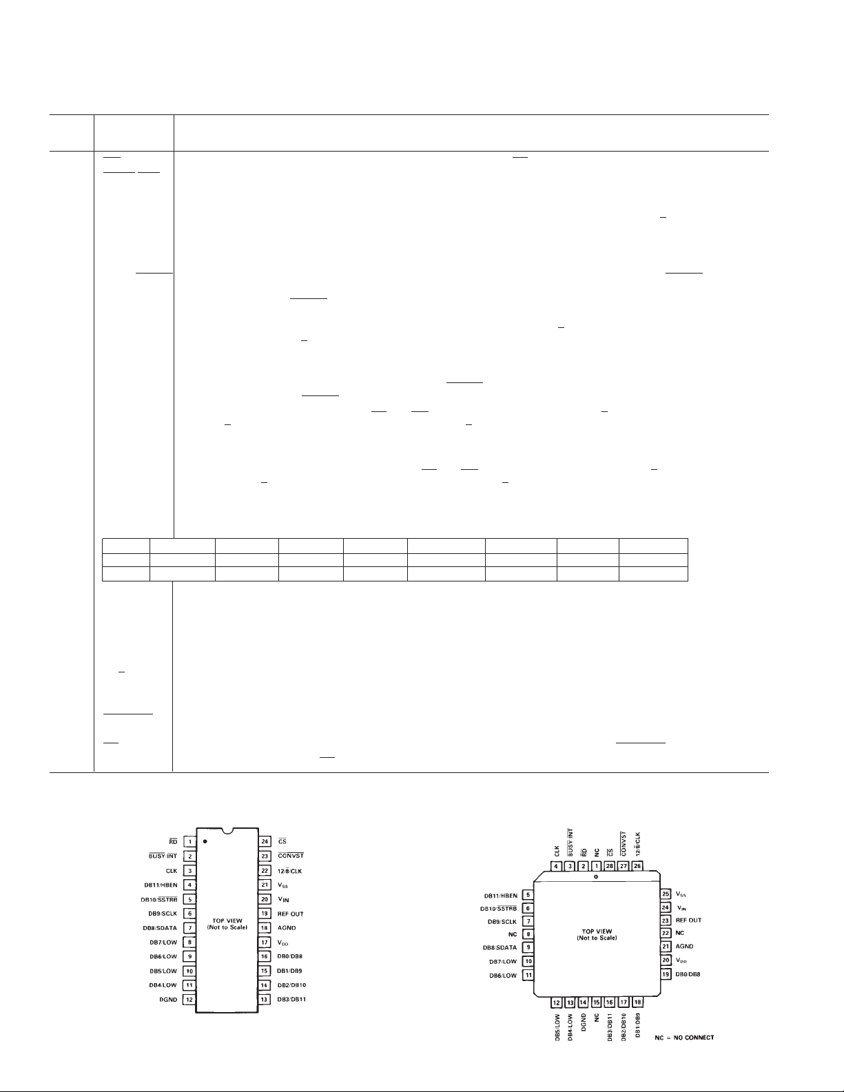
PIN FUNCTION DESCRIPTION
DIP Pin
Pin No. Mnemonic Function
1
2
RD Read. Active low logic input. This input is used in conjunction with CS low to enable the data outputs.
BUSY/INT Busy/Interrupt, Active low logic output indicating converter status. See timing diagrams.
3 CLK Clock input. An external TTL-compatible clock may be applied to this input pin. Alternatively, tying this pin to
V
enables the internal laser-trimmed clock oscillator.
4 DB11/HBEN Data Bit 11 (MSB)/High Byte Enable. The function of this pin is dependent on the state of the 12/
SS
8/CLK input (see
below). When 12-bit parallel data is selected, this pin provides the DB11 output. When byte data is selected, this pin
becomes the HBEN logic input HBEN is used for 8-bit bus interfacing. When HBEN is low, DB7/LOW to DB0/DB8
become DB7 to DB0. With HBEN high, DB7/LOW to DB0/DB8 are used for the upper byte of data (see Table I).
5 DB10/
SSTRB Data Bit 10/Serial Strobe. When 12-bit parallel data is selected, this pin provides the DB10 output. SSTRB is an
active low open-drain output that provides a strobe or framing pulse for serial data. An external 4.7 kΩ pull-up
resistor is required on
SSTRB.
6 DB9/SCLK Data Bit 9/Serial Clock. When 12-bit parallel data is selected, this pin provides the DB9 output. SCLK is the gated
serial clock output derived from the internal or external ADC clock. If the 12/
runs continuously. If 12/
8/CLK is at 0 V, then SCLK is gated off after serial transmission is complete. SCLK is an
8/CLK input is at –5 V, then SCLK
open-drain output and requires an external 2 kΩ pull-up resistor.
7 DB8/SDATA Data Bit 8/Serial Data. When 12-bit parallel data is selected, this pin provides the DB8 output. SDATA is an open-
drain serial data output which is used with SCLK and
ing edge of SCLK while
8–11 DB7/LOW– Three-state data outputs controlled by
DB4/LOW With 12/
8/CLK high, they are always DB7–DB4. With 12/8/CLK low or –5 V, their function is controlled by HBEN
SSTRB is low. An external 4.7 kΩ pull-up resistor is required on SDATA.
CS and RD. Their function depends on the 12/8/CLK and HBEN inputs.
SSTRB for serial data transfer. Serial data is valid on the fall-
(see Table I).
12 DGND Digital Ground. Ground reference for digital circuitry.
13–16 DB3/DB11– Three-state data outputs which are controlled by
DB0/DB8 inputs. With 12/
8/CLK high, they are always DB3–DB0. With 12/8/CLK low or –5 V, their function is controlled by
CS and RD. Their function depends on the 12/8/CLK and HBEN
HBEN (see Table I).
Table I. Output Data for Byte Interfacing
HBEN DB7/LOW DB6/LOW DB5/LOW DB4/LOW DB3/DB11 DB2/DB10 DB1/DB9 DB0/DB8
HIGH LOW LOW LOW LOW DB11(MSB) DB10 DB9 DB8
LOW DB7 DB6 DB5 DB4 DB3 DB2 DB1 DB0 (LSB)
17 V
DD
Positive Supply, +5 V ± 5%.
18 AGND Analog Ground. Ground reference for track/hold, reference and DAC.
19 REF OUT Voltage Reference Output. The internal 3 V reference is provided at this pin. The external load capability is 500 µA.
20 V
21 V
22 12/
IN
SS
8/CLK Three Function Input. Defines the data format and serial clock format. With this pin at +5 V, the output data for-
Analog Input. The analog input range is ±3 V for the AD7870, ±10 V for the AD7876 and 0 V to +5 V for the AD7875.
Negative Supply, –5 V ± 5%.
mat is 12-bit parallel only. With this pin at 0 V, either byte or serial data is available and SCLK is not continuous.
With this pin at –5 V, either byte or serial data is again available but SCLK is now continuous.
23
CONVST Convert Start. A low to high transition on this input puts the track/hold into its hold mode and starts conversion.
This input is asynchronous to the CLK input.
24
CS Chip Select. Active low logic input. The device is selected when this input is active. With CONVST tied low, a new
conversion is initiated when CS goes low.
1
PLCC
2
DIP and SOIC
2
PIN CONFIGURATIONS
1
PIN CONFIGURATIONS ARE THE SAME FOR
THE AD7875 AND AD7876.
2
THE AD7870 AND AD7875 ARE AVAILABLE IN
DIP AND PLCC; THE AD7870A IS AVAILABLE IN
PLASTIC DIP; THE AD7875 AND AD7876 ARE
AVAILABLE IN SOIC AND DIP.
–6–
REV. B
AD7870/AD7875/AD7876
CONVERTER DETAILS
The AD7870/AD7875/AD7876 is a complete 12-bit A/D converter, requiring no external components apart from power
supply decoupling capacitors. It is comprised of a 12-bit successive approximation ADC based on a fast settling voltage
output DAC, a high speed comparator and SAR, a track/hold
amplifier, a 3 V buried Zener reference, a clock oscillator and
control logic.
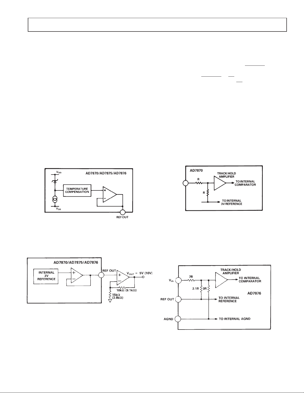
INTERNAL REFERENCE
The AD7870/AD7875/AD7876 has an on-chip temperature
compensated buried Zener reference that is factory trimmed to
3 V ±10 mV. Internally it provides both the DAC reference
and the d c bias required for bipolar operation (AD7870 and
AD7876). The reference output is available (REF OUT) and
capable of providing up to 500 µA to an external load.
The maximum recommended capacitance on REF OUT for
normal operation is 50 pF. If the reference is required for use
external to the ADC, it should be decoupled with a 200 Ω
resistor in series with a parallel combination of a 10 µF tanta-
lum capacitor and a 0.1 µF ceramic capacitor. These decoupling
components are required to remove voltage spikes caused by
the ADC’s internal operation.
to the conversion time plus the track/hold amplifier
acquisition time. For a 2.5 MHz input clock the throughput
rate is 10 µs max.
The operation of the track/hold is essentially transparent to the
user. The track/hold amplifier goes from its tracking mode to its
hold mode at the start of conversion. If the
used to start conversion then the track to hold transition occurs
on the rising edge of
transition occurs on the falling edge of
ANALOG INPUT
The three parts differ from each other in the analog input voltage range that they can handle. The AD7870 accepts ±3 V
input signals, the AD7876 accepts a ± 10 V input range, while
the input range for the AD7875 is 0 V to +5 V.
Figure 5a shows the AD7870 analog input. The analog input
range is ±3 V into an input resistance of typically 15 kΩ. The
designed code transitions occur midway between successive
integer LSB values (i.e., 1/2 LSB, 3/2 LSBs, 5/2 LSBs . . .
FS–3/2 LSBs). The output code is twos complement binary
with 1 LSB = FS/4096 = 6 V/4096 = 1.46 mV. The ideal input/
output transfer function is shown in Figure 6.
CONVST. If CS starts conversion, this
CONVST input is
CS.
2
Figure 3. Reference Circuit
The reference output voltage is 3 V. For applications using the
AD7875 or AD7876, a 5 V or 10 V reference may be required.
Figure 4 shows how to scale the 3 V REF OUT voltage to provide either a 5 V or 10 V external reference.
Figure 4. Generating a 5 V or 10 V Reference
TRACK-AND-HOLD AMPLIFIER
The track-and-hold amplifier on the analog input of the AD7870/
AD7875/AD7876 allows the ADC to accurately convert input
frequencies to 12-bit accuracy. The input bandwidth of the
track/hold amplifier is much greater than the Nyquist rate of the
ADC even when the ADC is operated at its maximum throughput rate. The 0.1 dB cutoff frequency occurs typically at 500
kHz. The track/hold amplifier acquires an input signal to 12-bit
accuracy in less than 2 µs. The overall throughput rate is equal
Figure 5a. AD7870 Analog Input
The AD7876 analog input structure is shown in Figure 5b. The
analog input range is ±10 V into an input resistance of typically
33 kΩ. As before, the designed code transitions occur midway
between successive integer LSB values. The output code is 2s
complement with 1 LSB = FS/4096 = 20 V/4096 = 4.88 mV.
The ideal input/output transfer function is shown in Figure 6.
Figure 5b. AD7876 Analog Input
Figure 5c shows the analog input for the AD7875. The input
range is 0 V to +5 V into an input resistance of typically 25 kΩ.
Once again, the designed code transitions occur midway
between successive integer LSB values. The output code is
REV. B
–7–

AD7870/AD7875/AD7876
straight binary with 1 LSB = FS/4096 = 5 V/4096 = 1.22 mV.
The ideal input/output transfer function is shown in Figure 7.
Figure 5c. AD7875 Analog Input
input voltage is 1/2 LSB below ground. The trim procedure is as
follows: apply a voltage of –0.73 mV(–1/2 LSB) at V
in Figure
1
8 and adjust the op amp offset voltage until the ADC output
code flickers between 1111 1111 1111 and 0000 0000 0000.
Gain error can be adjusted at either the first code transition
(ADC negative full-scale) or the last code transition (ADC positive full scale). The trim procedures for both cases are as follows
(see Figure 8).
Figure 8. Offset and Full-Scale Adjust Circuit
Figure 6. AD7870/AD7876 Transfer Function
Figure 7. AD7875 Transfer Function
OFFSET AND FULL-SCALE ADJUSTMENT—AD7870
In most digital signal processing (DSP) applications, offset and
full-scale errors have little or no effect on system performance.
Offset error can always be eliminated in the analog domain by
ac coupling. Full-scale error effect is linear and does not cause
problems as long as the input signal is within the full dynamic
range of the ADC. Some applications will require that the input
signal span the full analog input dynamic range. In such applications, offset and full-scale error will have to be adjusted to zero.
Where adjustment is required, offset error must be adjusted before full-scale error. This is achieved by trimming the offset of
the op amp driving the analog input of the AD7870 while the
Positive Full-Scale Adjust
Apply a voltage of 2.9978 V (FS/2 – 3/2 LSBs) at V1. Adjust R2
until the ADC output code flickers between 0111 1111 1110
and 0111 1111 1111.
Negative Full-Scale Adjust
Apply a voltage of –2.9993 V (–FS/2 + 1/2 LSB) at V1 and adjust R2 until the ADC output code flickers between 1000 0000
0000 and 1000 0000 0001.
OFFSET AND FULL-SCALE ADJUSTMENT—AD7876
The offset and full-scale adjustment for the AD7876 is similar
to that just outlined for the AD7870. The trim procedure, for
those applications that do require adjustment, is as follows:
apply a voltage of –2.44 mV (–1/2 LSB) at V
and adjust the op
1
amp offset voltage until the ADC output code flickers between
1111 1111 1111 and 0000 0000 0000. Full-scale error can be
adjusted at either the first code transition (ADC negative full
scale) or the last code transition (ADC positive full scale). The
trim procedure for both case is as follows (see Figure 8):
Positive Full-Scale Adjust
Apply a voltage of 9.9927 V (FS/2 –3/2 LSBs) at V1. Adjust R2
until the ADC output code flickers between 0111 1111 1110
and 0111 1111 1111.
Negative Full-Scale Adjust
Apply a voltage of –9.9976 V (FS/2 + 1/2 LSB) at V1 and adjust
R2 until the ADC output code flickers between 1000 0000 0000
and 1000 0000 0001.
–8–
REV. B
AD7870/AD7875/AD7876
OFFSET AND FULL-SCALE ADJUSTMENT—AD7875
Similar to the AD7870, most of the DSP applications in which
the AD7875 will be used will not require offset and full-scale
adjustment. For applications that do require adjustment, offset
error must be adjusted before full-scale (gain) error. This is
achieved by applying an input voltage of 0.61 mV (1/2 LSB) to
V
in Figure 8 and adjusting the op amp offset voltage until the
1
ADC output code flickers between 0000 0000 0000 and 0000
0000 0001. For full-scale adjustment, apply an input voltage of
4.9982 V (FS – 3/2 LSBs) to V
output code flickers between 1111 1111 1110 and 1111 1111
1111.
TIMING AND CONTROL
The AD7870/AD7875/AD7876 is capable of two basic operating
modes. In the first mode (Mode 1), the
start conversion and drive the track/hold into its hold mode. At
the end of conversion the track/hold returns to its tracking mode.
It is intended principally for digital signal processing and other
applications where precise sampling in time is required. In these
applications, it is important that the signal sampling occurs at exactly equal intervals to minimize errors due to sampling uncertainty or jitter. For these cases, the
timer or some precise clock source.
The second mode is achieved by hard-wiring the
low. This mode (Mode 2) is intended for use in systems where
the microprocessor has total control of the ADC, both initiating
the conversion and reading the data.
the microprocessor will normally be driven into a WAIT state
for the duration of conversion by
DATA OUTPUT FORMATS
In addition to the two operating modes, the AD7870/AD7875/
AD7876 also offers a choice of three data output formats, one
serial and two parallel. The parallel data formats are a single,
12-bit parallel word for 16-bit data buses and a two-byte format
for 8-bit data buses. The data format is controlled by the 12/
CLK input. A logic high on this pin selects the 12-bit parallel
output format only. A logic low or –5 V applied to this pin allows the user access to either serial or byte formatted data.
Three of the pins previously assigned to the four MSBs in parallel form are now used for serial communications while the
fourth pin becomes a control input for the byte-formatted data.
The three possible data output formats can be selected in either
of the modes of operation.
Parallel Output Format
The two parallel formats available on the part are a 12-bit wide
data word and a two-byte data word. In the first, all 12 bits of
data are available at the same time on DB11 (MSB) through
DB0 (LSB). In the second, two reads are required to access the
data. When this data format is selected, the DB11/HBEN pin
assumes the HBEN function. HBEN selects which byte of data
is to be read from the ADC. When HBEN is low, the lower
eight bits of data are placed on the data bus during a read operation; with HBEN high, the upper four bits of the 12-bit word
are placed on the data bus. These four bits are right justified
and thereby occupy the lower nibble of data while the upper
nibble contains four zeros.
Serial Output Format
Serial data is available on the AD7870/AD7875/AD7876 when
the 12/
8/CLK input is at 0 V or –5 V and in this case the DB10/
SSTRB, DB9/SCLK and DB8/SDATA pins assume their serial
REV. B
and adjust R2 until the ADC
1
CONVST line is used to
CONVST line is driven by a
CONVST line
CS starts conversion and
BUSY/INT.
8/
–9–
functions. Serial data is available during conversion with a word
length of 16 bits; four leading zeros, followed by the 12-bit conversion result starting with the MSB. The data is synchronized
to the serial clock output (SCLK) and framed by the serial
strobe (
SSTRB). Data is clocked out on a low to high transition
of the serial clock and is valid on the falling edge of this clock
while the
clock cycles after
leading zero) is valid on the first falling edge of SCLK. All three
serial lines are open-drain outputs and require external pull-up
resistors.
The serial clock out is derived from the ADC clock source,
which may be internal or external. Normally, SCLK is required
during the serial transmission only. In these cases, it can be shut
down at the end of conversion to allow multiple ADCs to share
a common serial bus. However, some serial systems (e.g.,
TMS32020) require a serial clock that runs continuously. Both
options are available on the AD7870/AD7875/AD7876 using
the 12/
(SCLK) runs continuously; when 12/
turned off at the end of transmission.
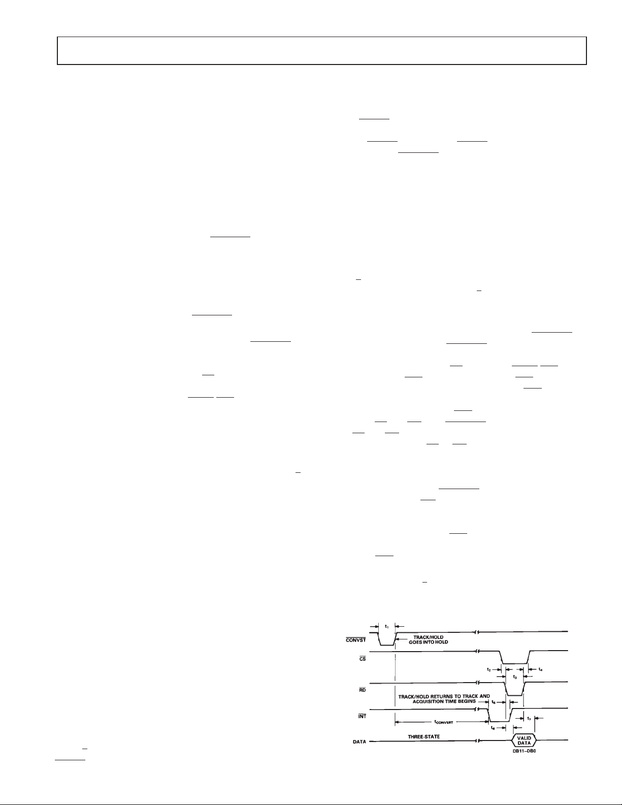
MODE 1 INTERFACE
Conversion is initiated by a low going pulse on the CONVST
input. The rising edge of this
and drives the track/hold amplifier into its hold mode. Conversion will not be initiated if the
output assumes its
high and goes low at the end of conversion. This
be used to interrupt the microprocessor. A read operation to the
ADC accesses the data and the
ing edge of
when
rectly in this mode. The
wired low in this mode. Data cannot be read from the part
during conversion because the on-chip latches are disabled
when conversion is in progress. In applications where precise
sampling is not critical, the
from a microprocessor
dress. In some applications, depending on power supply turn-on
time, the AD7870/AD7875/AD7876 may perform a conversion
on power-up. In this case, the
dummy read to the AD7870/AD7875/AD7876 will be required
to reset the
Figure 9 shows the Mode 1 timing diagram for a 12-bit parallel
data output format (12/
the end of conversion accesses all 12 bits of data at the same
time. Serial data is not available for this data output format.
SSTRB output is low. SSTRB goes low within three
CONVST, and the first serial data bit (the first
8/CLK input. With this input at –5 V, the serial clock
8/CLK is at 0 V, SCLK is
CONVST pulse starts conversion
CS is low. The BUSY/INT status
INT function in this mode. INT is normally
INT line can
INT line is reset high on the fall-
CS and RD. The CONVST input must be high
CS and RD are brought low for the ADC to operate cor-
CS or RD input should not be hard-
CONVST pulse can be generated
WR line OR-gated with a decoded ad-
INT line will power-up low and a
INT line before starting conversion.
8/CLK = +5 V). A read to the ADC at
Figure 9. Mode 1 Timing Diagram, 12-Bit Parallel Read
2

AD7870/AD7875/AD7876
Figure 10. Mode 1 Timing Diagram, Byte or Serial Read
The Mode 1 timing diagram for byte and serial data is shown in
Figure 10.
high by the first falling edge of
end of conversion can either access the low byte or high byte of
data depending on the status of HBEN (Figure 10 shows low
byte only for example). The diagram shows both a noncontinuously and a continuously running clock (dashed line).
MODE 2 INTERFACE
The second interface mode is achieved by hard wiring CONVST
low and conversion is initiated by taking
low. The track/hold amplifier goes into the hold mode on the
falling edge of
INT goes low at the end of conversion and is reset
CS and RD. This first read at the
CS low while HBEN is
CS. In this mode, the BUSY/INT pin assumes
its BUSY function. BUSY goes low at the start of conversion,
stays low during the conversion and returns high when the conversion is complete. It is normally used in parallel interfaces to
drive the microprocessor into a WAIT state for the duration of
conversion.
Figure 11 shows the Mode 2 timing diagram for the 12-bit parallel data output format (12/
ADC behaves like slow memory. The major advantage of this
interface is that it allows the microprocessor to start conversion,
WAIT and then read data with a single READ instruction. The
user does not have to worry about servicing interrupts or ensuring that software delays are long enough to avoid reading during
conversion.
8/CLK = +5 V). In this case, the
Figure 11. Mode 2 Timing Diagram, 12-Bit Parallel Read
–10–
REV. B

AD7870/AD7875/AD7876
Figure 12. Mode 2 Timing Diagram, Byte or Serial Read
2
The Mode 2 timing diagram for byte and serial data is shown in
Figure 12. For two-byte data read, the lower byte (DB0–DB7)
has to be accessed first since HBEN must be low to start conversion. The ADC behaves like slow memory for this first read,
but the second read to access the upper byte of data is a normal
read. Operation of the serial functions is identical between
Mode 1 and Mode 2. The timing diagram of Figure 12 shows
both a noncontinuously and a continuously running SCLK
(dashed line).
DYNAMIC SPECIFICATIONS
The AD7870 and AD7875 are specified and 100% tested for
dynamic performance specifications as well as traditional dc
specifications such as integral and differential nonlinearity. Although the AD7876 is not production tested for ac parameters,
its dynamic performance is similar to the AD7870 and AD7875.
The ac specifications are required for signal processing applications such as speech recognition, spectrum analysis and high
speed modems. These applications require information on the
ADC’s effect on the spectral content of the input signal. Hence,
the parameters for which the AD7870 and AD7875 are specified include SNR, harmonic distortion, intermodulation distortion and peak harmonics. These terms are discussed in more
detail in the following sections.
Signal-to-Noise Ratio (SNR)
SNR is the measured signal-to-noise ratio at the output of the
ADC. The signal is the rms magnitude of the fundamental.
Noise is the rms sum of all the nonfundamental signals up to
half the sampling frequency (FS/2) excluding dc. SNR is dependent upon the number of quantization levels used in the digitization process; the more levels, the smaller the quantization
noise. The theoretical signal-to-noise ratio for a sine wave input
is given by
SNR = (6.02N + 1.76) dB (1)
where N is the number of bits. Thus for an ideal 12-bit converter, SNR = 74 dB.
sine-wave signal of very low distortion to the V
sampled at a 100 kHz sampling rate. A Fast Fourier Transform
(FFT) plot is generated from which the SNR data can be obtained. Figure 13 shows a typical 2048 point FFT plot of the
AD7870KN/AD7875KN with an input signal of 25 kHz and a
sampling frequency of 100 kHz. The SNR obtained from this
graph is 72.6 dB. It should be noted that the harmonics are
taken into account when calculating the SNR.
Figure 13. FFT Plot
Effective Number of Bits
The formula given in (1) relates SNR to the number of bits.
Rewriting the formula, as in (2), it is possible to get a measure
of performance expressed in effective number of bits (N).
SNR – 1.76
N = (2)
The effective number of bits for a device can be calculated directly from its measured SNR.
6.02
input which is
IN
REV. B
–11–

AD7870/AD7875/AD7876
Figure 14 shows a typical plot of effective number of bits versus
frequency for an AD7870KN/AD7875KN with a sampling frequency of 100 kHz. The effective number of bits typically falls
between 11.7 and 11.85 corresponding to SNR figures of 72.2
and 73.1 dB.
Figure 14. Effective Number of Bits vs. Frequency
Total Harmonic Distortion (THD)
THD is the ratio of the rms sum of harmonics to the rms value
of the fundamental. For the AD7870/AD7875, THD is defined
as
2
THD = 20 log
V
2
+V
2
+V
3
V
where V1 is the rms amplitude of the fundamental and V2, V3,
V
, V5 and V6 are the rms amplitudes of the second through the
4
sixth harmonic. The THD is also derived from the FFT plot of
the ADC output spectrum.
Intermodulation Distortion
With inputs consisting of sine waves at two frequencies, fa and
fb, any active device with nonlinearities will create distortion
products at sum and difference frequencies of mfa ± nfb where
m, n = 0, 1, 2, 3, etc. Intermodulation terms are those for which
neither m nor n are equal to zero. For example, the second order terms include (fa + fb) and (fa – fb), while the third order
terms include (2fa + fb), (2fa – fb), (fa + 2fb) and (fa – 2fb).
Using the CCIF standard, where two input frequencies near the
top end of the input bandwidth are used, the second and third
order terms are of different significance. The second order terms
are usually distanced in frequency from the original sine waves
while the third order terms are usually at a frequency close to
the input frequencies. As a result, the second and third order
terms are specified separately. The calculation of the intermodulation distortion is as per the THD specification where it is the
ratio of the rms sum of the individual distortion products to the
rms amplitude of the fundamental expressed in dBs. In this
case, the input consists of two, equal amplitude, low distortion
sine waves. Figure 15 shows a typical IMD plot for the AD7870/
AD7875.
Peak Harmonic or Spurious Noise
Peak harmonic or spurious noise is defined as the ratio of the
rms value of the next largest component in the ADC output
spectrum (up to FS/2 and excluding dc) to the rms value of the
fundamental. Normally, the value of this specification will be
determined by the largest harmonic in the spectrum, but for
parts where the harmonics are buried in the noise floor the peak
will be a noise peak.
2
2
+V
4
1
2
+V
5
6
Figure 15. IMD Plot
AC Linearity Plot
When a sine wave of specified frequency is applied to the V
IN
input of the AD7870/AD7875 and several million samples are
taken, a histogram showing the frequency of occurrence of each
of the 4096 ADC codes can be generated. From this histogram
data it is possible to generate an ac integral linearity plot as
shown in Figure 16. This shows very good integral linearity performance from the AD7870/AD7875 at an input frequency of
25 kHz. The absence of large spikes in the plot shows good differential linearity. Simplified versions of the formulae used are
outlined below.
INL(i) =
V(i)–V(o)
V(fs)–V(o)
⋅ 4096
–i
where INL(i) is the integral linearity at code i. V(fs) and V(o)
are the estimated full-scale and offset transitions and V(i) is the
estimated transition for the i
th
code.
V(i) the estimated code transition point is derived as follows:
π⋅cum(i )
V(i) = –A • Cos
[]
N
where A is the peak signal amplitude,
N is the number of histogram samples
and cum(i) = Σ
i
V(n) occurrences
n=0
–12–
Figure 16. AC INL Plot
REV. B

MICROPROCESSOR INTERFACE
The AD7870/AD7875/AD7876 has a wide variety of interfacing
options. It offers two operating modes and three data-output formats. Fast data access times allow direct interfacing to most microprocessors including the DSP processors.
Parallel Read Interfacing
Figures 17 to 19 show interfaces to the ADSP-2100, TMS32010
and the TMS32020 DSP processors. The ADC is operating in
Mode 1, parallel read for all three interfaces. An external timer
controls conversion start asynchronously to the microprocessor.
At the end of each conversion the ADC
the microprocessor. The conversion result is read from the ADC
with the following instruction:
ADSP-2100: MR0 = DM(ADC)
TMS32010: IN D,ADC
TMS32020: IN D,ADC
MR0 = ADSP-2100 MR0 Register
D = Data Memory Address
ADC = AD7870/AD7875/AD7876 Address
Some applications may require that conversions be initiated by
the microprocessor rather than an external timer. One option is
to decode the
write operation to the ADC starts a conversion. Data is read at
the end of conversion as described earlier. Note: a read operation
must not be attempted during conversion.
CONVST signal from the address bus so that a
Figure 17. ADSP-2100 Parallel Interface
BUSY/INT interrupts
AD7870/AD7875/AD7876
Figure 19. TMS32020 Parallel Interface
Two Byte Read Interfacing
68008 Interface
Figure 20 shows an 8-bit bus interface for the MC68008 microprocessor. For this interface, the 12/
and the DB11/HBEN pin is driven from the microprocessor
least significant address bit. Conversion start control is provided
by the microprocessor. In this interface example, a Move instruction from the ADC address both starts a conversion and
reads the conversion result.
MOVEW ADC,DO
ADC = AD7870/AD7875/AD7876 address
D0 = 68008 D0 register
This is a two byte read instruction. During the first read opera-
tion
BUSY, in conjunction with CS, forces the microprocessor
to WAIT for the ADC conversion. At the end of conversion the
ADC low byte (DB7–DB0) is loaded into D15–D8 of the D0
register and the ADC high byte (DB15–DB7) is loaded into
D7–D0 of the D0 register. The following Rotate instruction to
the D0 register swaps the high and low bytes to the correct
format.
R0L = 8, D0.
Note: while executing the two byte read instruction above,
WAIT states are inserted during the first read operation only
and not for the second.
8/CLK input is tied to 0 V
2
REV. B
Figure 18. TMS32010 Parallel Interface
Figure 20. MC68008 Byte Interface
–13–
AD7870/AD7875/AD7876
Serial Interfacing
Figures 21 to 24 show the AD7870/AD7875/AD7876 configured for serial interfacing. In all four interfaces, the ADC is configured for Mode 1 operation. The interfaces show a timer
driving the
decoded address if required. The SCLK, SDAT and
open-drain outputs. If these are required to drive capacitive
loads in excess 35 pF, buffering is recommended.
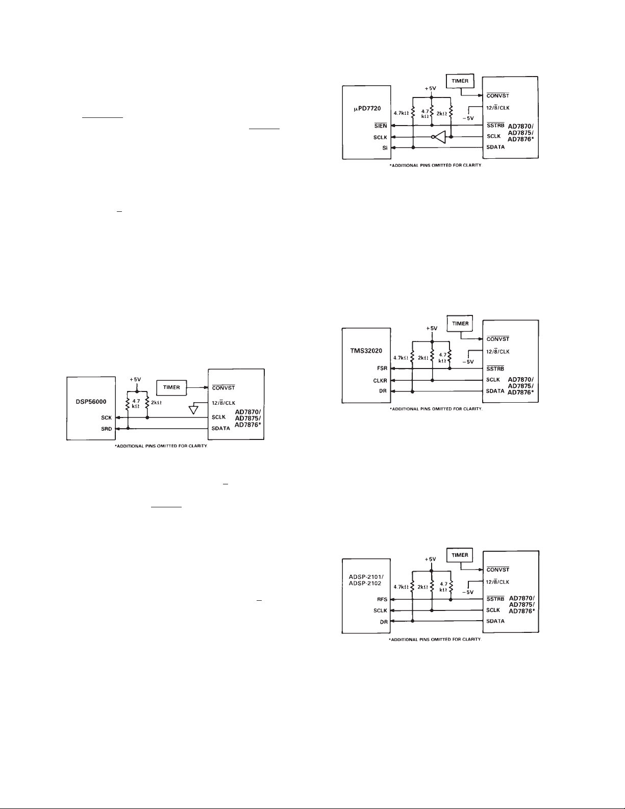
DSP56000 Serial Interface
Figure 21 shows a serial interface between the AD7870/
AD7875/AD7876 and the DSP56000. The interface arrangement is two-wire with the ADC configured for noncontinuous
clock operation (12/
ured for normal mode asynchronous operation with gated clock.
It is also set up for a 16-bit word with SCK and SC1 as inputs
and the FSL control bit set to a 0. In this configuration, the
DSP56000 assumes valid data on the first falling edge of SCK.
Since the ADC provides valid data on this first edge, there is no
need for a strobe or framing pulse for the data. SCLK and
SDATA are gated off when the ADC is not performing a conversion. During conversion, data is valid on the SDATA output
of the ADC and is clocked into the receive data shift register of
the DSP56000. When this register has received 16 bits of data,
it generates an internal interrupt on the DSP56000 to read the
data from the register.
CONVST input, but this could be generated from a
SSTRB are
8/CLK = 0 V). The DSP56000 is config-
Figure 22. NEC7720 Serial Interface
TMS32020 Serial Interface
Figure 23 shows a serial interface between the AD7870/ AD7875/
AD7876 and the TMS32020. The AD7870/AD7875/AD7876 is
configured for continuous clock operation. Note, the ADC will
not interface correctly to the TMS32020 if the ADC is configured for a noncontinuous clock. Data is clocked into the data
receive register (DRR) of the TMS32020 during conversion. As
with the previous interfaces, when a 16-bit word is received by
the TMS32020 it generates an internal interrupt to read the
data from the DRR.
Figure 21. DSP56000 Serial Interface
The DSP56000 and AD7870/AD7875/AD7876 can also be
configured for continuous clock operation (12/
In this case, a strobe pulse is required by the DSP56000 to indicate when data is valid. The
verted and applied to the SC1 input of the DSP56000 to
provide this strobe pulse. All other conditions and connections
are the same as for gated clock operation.
NEC7720/77230 Serial Interface
A serial interface between the AD7870/AD7875/AD7876 and
the NEC7720 is shown in Figure 22. In the interface shown, the
ADC is configured for continuous clock operation. This can be
changed to a noncontinuous clock by simply tying the 12/
input of the ADC to 0 V with all other connections remaining
the same. The NEC7720 expects valid data on the rising edge of
its SCK input and therefore an inverter is required on the
SCLK output of the ADC. The NEC7720 is configured for a
16-bit data word. Once the 16 bits of data have been received
by the SI register of the NEC7720, an internal interrupt is generated to read the contents of the SI register.
The NEC77230 interface is similar to that just outlined for the
NEC7720. However, the clock input of the NEC77230 is
SICLK. Additionally, no inverter is required between the ADC
SCLK output and this SICLK input since the NEC77230 assumes data is valid on the falling edge of SICLK.
SSTRB output of the ADC is in-
8/CLK = –5 V).
8/CLK
Figure 23. TMS32020 Serial Interface
ADSP-2101/ADSP-2102 Serial Interface
Figure 24 shows a serial interface between the AD7870/AD7875/
AD7876 and the ADSP-2101/ADSP-2102. The ADC is configured for continuous clock operation. Data is clocked into the
serial port register of the ADSP-2101/ADSP-2102 during conversion. As with the previous interfaces, when a 16-bit data
word is received by the ADSP-2101/ADSP-2102 an internal microprocessor interrupt is generated and the data is read from the
serial port register.
Figure 24. ADSP-2101/ADSP-2102 Serial Interface
–14–
REV. B

AD7870/AD7875/AD7876
STAND-ALONE OPERATION
The AD7870/AD7875/AD7876 can be used in its Mode 2, parallel interface mode for stand-alone operation. In this case, conversion is initiated with a pulse to the ADC
pulse must be longer than the conversion time of the ADC. The
BUSY output is used to drive the RD input. Data is latched
from the ADC DB0–DB11 outputs to an external latch on the
rising edge of
APPLICATION HINTS
Good printed circuit board (PCB) layout is as important as the
overall circuit design itself in achieving high speed A/D performance. The designer has to be conscious of noise both in the
ADC itself and in the preceding analog circuitry. Switching
mode power supplies are not recommended as the switching
spikes will feed through to the comparator causing noisy code
transitions. Other causes of concern are ground loops and digital feedthrough from microprocessors. These are factors which
influence any ADC, and a proper PCB layout which minimizes
these effects is essential for best performance.
LAYOUT HINTS
Ensure that the layout for the printed circuit board has the digital and analog signal lines separated as much as possible. Take
care not to run any digital track alongside an analog signal track.
Guard (screen) the analog input with AGND.
Establish a single point analog ground (star ground) separate
from the logic system ground at the AGND pin or as close as
possible to the ADC. Connect all other grounds and the
AD7870/AD7875/AD7876 DGND to this single analog ground
point. Do not connect any other digital grounds to this analog
ground point.
Low impedance analog and digital power supply common returns are essential to low noise operation of the ADC, so make
the foil width for these tracks as wide as possible. The use of
ground planes minimizes impedance paths and also guards the
analog circuitry from digital noise. The circuit layout of Figures
30 and 31 have both analog and digital ground planes which are
kept separated and only joined together at the AD7870/
AD7875/AD7876 AGND pin.
BUSY.
Figure 25. Stand-Alone Operation
CS input. This
grounds between the signal source and the ADC appears as an
error voltage in series with the input signal.
DATA ACQUISITION BOARD
Figure 28 shows the AD7870/AD7875/AD7876 in a data acquisition circuit. The corresponding printed circuit board (PCB)
layout and silkscreen are shown in Figures 29 to 31. The board
layout has three interface ports: one serial and two parallel. One
of the parallel ports is directly compatible with the ADSP-2100
evaluation board expansion connector.
The only additional component required for a full data acquisition system is an antialiasing filter. A component grid is provided near the analog input on the PCB, which may be used for
such a filter or any other input conditioning circuitry. To facilitate this option there is a shorting plug (labelled LK1 on the
PCB) on the analog input track. If this shorting plug is used, the
analog input connects to the buffer amplifier driving the ADC;
if this shorting plug is omitted, a wire link can be used to connect the analog input to the PCB component grid.
INTERFACE CONNECTIONS
There are two parallel connectors labeled SKT4 and SKT6 and
one serial connector labeled SKT5. A shorting plug option
(LK3 in Figure 28) on the ADC 12/
the ADC for the appropriate interface (see Pin Function
Description).
SKT6 is a 96-contact (3-ROW) Eurocard connector that is
directly compatible with the ADSP-2100 Evaluation Board
Prototype Expansion Connector. The expansion connector on
the ADSP-2100 has eight decoded chip enable outputs labeled
ECE1 to ECE8. ECE6 is used to drive the ADC CS input on
the data acquisition board. To avoid selecting on board RAM
sockets at the same time, LK6 on the ADSP-2100 board must
be removed. In addition, the ADSP-2100 expansion connector
has four interrupts labelled
INT output connects to EIRQ0. There is a single wait state gen-
erator connected to EDMACK to allow the ADC to interface to
the faster versions of the ADSP-2100.
SKT4 is a 26-way (2-ROW) IDC connector. This connector
contains all the signal contacts as SKT6 with the exception of
EDMACK which is connected to SKT6 only. It also contains
decoded R/
TMS32020 interfacing. The SKT4 pinout is shown in Figure 26.
W and STRB inputs which are necessary for
EIRQ0 to EIRQ3. The ADC BUSY/
8/CLK input configures
2
NOISE
Keep the input signal leads to VIN and signal return leads from
AGND as short as possible to minimize input noise coupling. In
applications where this is not possible, use a shielded cable between the source and the ADC. Reduce the ground circuit impedance as much as possible since any potential difference in
REV. B
–15–
Figure 26. SKT4, IDC Connector Pinout
AD7870/AD7875/AD7876
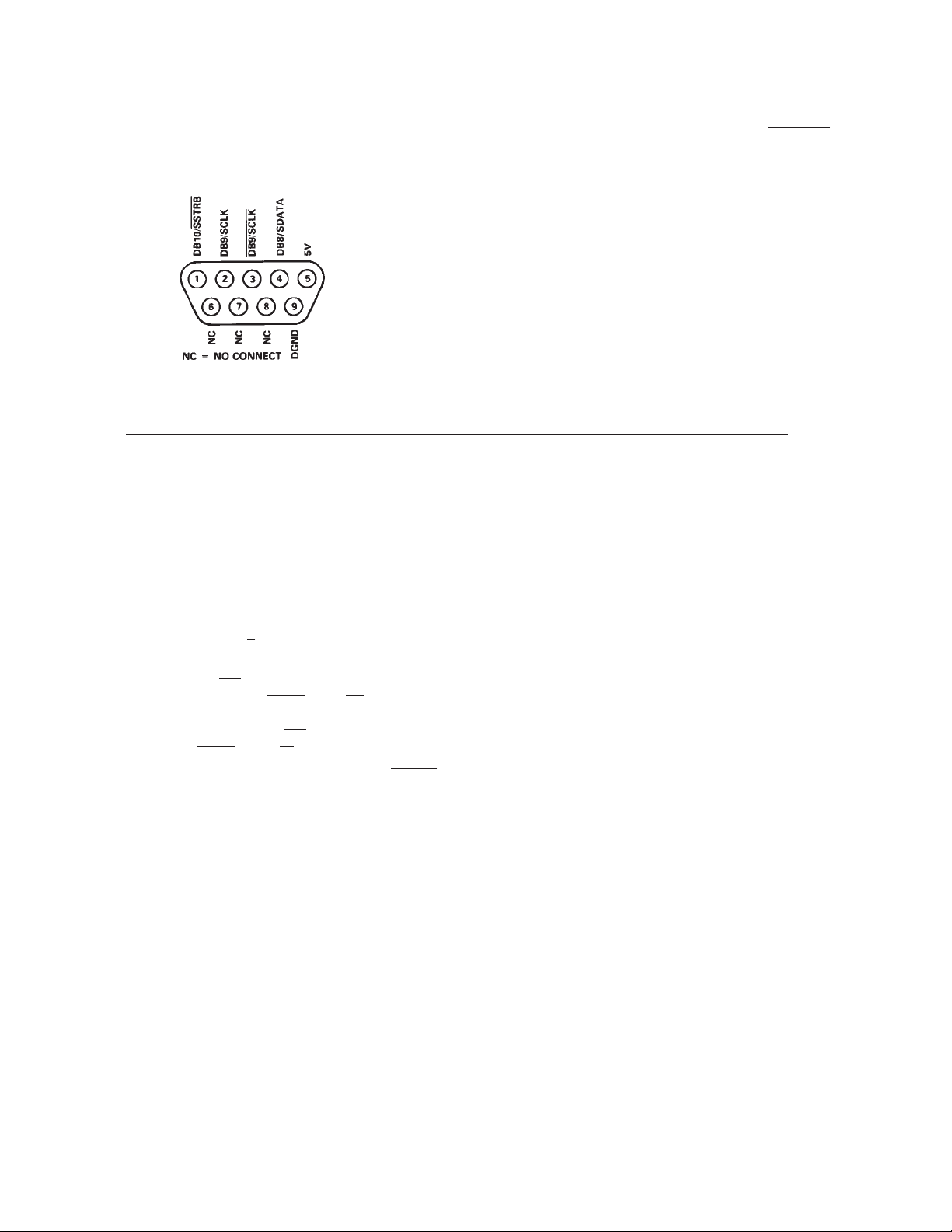
SKT5 is a 9-way D-type connector that is meant for serial interfacing only. An inverted DB9/SCLK output is also provided on
this connector for systems that accept data on a rising clock
edge. The SKT5 pinout is shown in Figure 27.
Figure 27. SKT5, D-Type Connector Pinout
SHORTING PLUG OPTIONS
There are seven shorting plug options that must be set before
using the board. These are outlined below:
LK1 Connects the analog input to a buffer amplifier. The
analog input may also be connected to a component grid
for signal conditioning.
LK2 Selects either the ADC internal clock or an external
clock source.
LK3 Configures the ADC 12/
ate serial or parallel interface.
LK4 Connects the ADC
connectors or to a decoded
shorting plug setting depends on the microprocessor e.g.,
the TMS32010 has a separate
TMS32020 has
LK5– Connect the pull-up resistors R3, R4 and R5 to
LK7 SCLK and SDATA. These shorting plugs should be
removed for parallel interfacing.
STRB and R/W outputs.
8/CLK input for the appropri-
RD input directly to the two parallel
STRB and R/W input. This
RD output while the
SSTRB,
SKT1, SKT2 and SKT3 are three BNC connectors which provide input connections for the analog input, the
and an external clock input. The use of an external clock source
is optional; there is a shorting plug (LK2) on the ADC CLK input that must be connected to either –5 V (for the ADCs own
internal clock) or to SKT3.
POWER SUPPLY CONNECTIONS
The PCB requires two analog power supplies and one 5 V digital supply . The analog supplies are labelled V+ and V–, and the
range for both supplies is 12 V to 15 V (see silkscreen in Figure
29). Connection to the 5 V digital supply is made through any
of the connectors (SKT4 to SKT6). The –5 V supply required
by the ADC is generated from a voltage regulator on the V–
power supply input (IC3 in Figure 27).
COMPONENT LIST
IC1 AD711 Op Amp
IC2 AD7870/AD7875/AD7876 Analog-to-
Digital Converter
IC3 MC79L05 –5 V Regulator
IC4 74HC00 Quad NAND Gate
IC5 74HC74 Dual D-Type Flip Flop
C1, C3, C5, C7, 10 µF Capacitors
C9, C11
C2, C4, C6, C8, 0.1 µF Capacitors
C10, C12
R1, R2 10 kΩ Pull-Up Resistors
R3*, R5* 4.7 kΩ Pull-Up Resistors
R4* 2 kΩ Pull-Up Resistor
LK1, LK2 Shorting Plugs
LK3, LK4
LK5, LK6, LK7
SKT1, SKT2, SKT3 BNC Sockets
SKT4 26-Contact (2-Row) IDC Connector
SKT5 9-Contact D-Type Connector
SKT6 96-Contact (3-Row) Eurocard Connector
*Required for Serial Communication only.
CONVST input
–16–
REV. B

AD7870/AD7875/AD7876
2
Figure 28. Data Acquisition Circuit Using the AD7870/AD7875/AD7876
REV. B
Figure 29. PCB Silkscreen for Figure 28
–17–

AD7870/AD7875/AD7876
Figure 30. PCB Component Side Layout for Figure 28
Figure 31. PCB Solder Side Layout for Figure 28
–18–
REV. B

OUTLINE DIMENSIONS
Dimensions shown in inches and (mm).
AD7870/AD7875/AD7876
24-Pin Plastic DIP (N-24)
24-Pin Cerdip (Q-24)
28-Pin PLCC (P-28A)
2
24-Pin SOIC (R-24)
REV. B
–19–

C1336–10–8/90
–20–
PRINTED IN U.S.A.
 Loading...