

LC2MOS 4-Channel, 12-Bit Simultaneous
AGND
CLK
DGND
DB11
DB0
V
SS
CS
12-BIT
DAC
V
IN1
V
IN2
V
IN3
V
IN4
COMP
REFERENCE
BUFFER
INT
RD
AD7874
CONVST
VDDV
DD
REF IN
REF OUT
3V
REFERENCE
DATA
REGISTERS
SAR
MUX
CONTROL LOGIC
INTERNAL
CLOCK
TRACK/
HOLD 3
TRACK/
HOLD 4
TRACK/
HOLD 2
TRACK/
HOLD 1
a
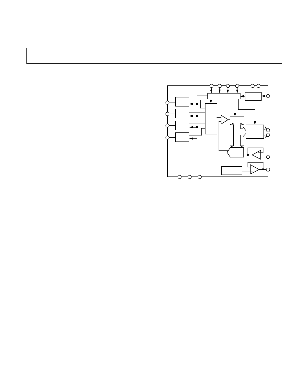
Sampling Data Acquisition System
AD7874
FEATURES
Four On-Chip Track/Hold Amplifiers
Simultaneous Sampling of 4 Channels
Fast 12-Bit ADC with 8 ms Conversion Time/Channel
29 kHz Sample Rate for All Four Channels
On-Chip Reference
610 V Input Range
65 V Supplies
APPLICATIONS
Sonar
Motor Controllers
Adaptive Filters
Digital Signal Processing
GENERAL DESCRIPTION
The AD7874 is a four-channel simultaneous sampling, 12-bit
data acquisition system. The part contains a high speed 12-bit
ADC, on-chip reference, on-chip clock and four track/hold amplifiers. This latter feature allows the four input channels to be
sampled simultaneously, thus preserving the relative phase
information of the four input channels, which is not possible if
all four channels share a single track/hold amplifier. This makes
the AD7874 ideal for applications such as phased-array sonar
and ac motor controllers where the relative phase information is
important.
The aperture delay of the four track/hold amplifiers is small and
specified with minimum and maximum limits. This allows several AD7874s to sample multiple input channels simultaneously
without incurring phase errors between signals connected to
several devices. A reference output/reference input facility also
allows several AD7874s to be driven from the same reference
source.
In addition to the traditional dc accuracy specifications such as
linearity, full-scale and offset errors, the AD7874 is also fully
specified for dynamic performance parameters including distortion and signal-to-noise ratio.
The AD7874 is fabricated in Analog Devices’ Linear Compatible CMOS (LC
that combines precision bipolar circuits with low-power CMOS
logic. The part is available in a 28-pin, 0.6" wide, plastic or hermetic dual-in-line package (DIP), in a 28-terminal leadless ceramic chip carrier (LCCC) and in a 28-pin SOIC.
REV. C
Information furnished by Analog Devices is believed to be accurate and
reliable. However, no responsibility is assumed by Analog Devices for its
use, nor for any infringements of patents or other rights of third parties
which may result from its use. No license is granted by implication or
otherwise under any patent or patent rights of Analog Devices.
2
MOS) process, a mixed technology process
PRODUCT HIGHLIGHTS
1. Simultaneous Sampling of Four Input Channels.
Four input channels, each with its own track/hold amplifier,
allow simultaneous sampling of input signals. Track/hold acquisition time is 2 µs, and the conversion time per channel is
8 µs, allowing 29 kHz sample rate for all four channels.
2. Tight Aperture Delay Matching.
The aperture delay for each channel is small and the aperture
delay matching between the four channels is less than 4 ns.
Additionally, the aperture delay specification has upper and
lower limits allowing multiple AD7874s to sample more than
four channels.
3. Fast Microprocessor Interface.
The high speed digital interface of the AD7874 allows direct
connection to all modern 16-bit microprocessors and digital
signal processors.
One Technology Way, P.O. Box 9106, Norwood, MA 02062-9106, U.S.A.
Tel: 617/329-4700 Fax: 617/326-8703
FUNCTIONAL BLOCK DIAGRAM

AD7874–SPECIFICA TIONS
(VDD = +5 V, VSS = –5 V, AGND = DGND = 0 V, REF IN = +3 V, f
external. All specifications T
MIN
to T
unless otherwise noted.)
MAX
= 2.5 MHz
CLK
Parameter A Version B Version S Version Units Test Conditions/Comments
SAMPLE-AND-HOLD
Acquisition Time2 to 0.01% 2 2 2 µs max
Droop Rate
–3 dB Small Signal Bandwidth
Aperture Delay
Aperture Jitter
Aperture Delay Matching
2, 3
2, 3
2
3
1 1 2 mV/ms max
500 500 500 kHz typ VIN = 500 mV p-p
0 0 0 ns min
40 40 40 ns max
2
200 200 200 ps typ
4 4 4 ns max
SAMPLE-AND-HOLD AND ADC
DYNAMIC PERFORMANCE
Signal-to-Noise Ratio 70 71 70 dB min fIN = 10 kHz Sine Wave, f
Total Harmonic Distortion –78 –80 –78 dB max fIN = 10 kHz Sine Wave, f
Peak Harmonic or Spurious Noise –78 –80 –78 dB max fIN = 10 kHz Sine Wave, f
Intermodulation Distortion fa = 9 kHz, fb = 9.5 kHz, f
SAMPLE
SAMPLE
SAMPLE
SAMPLE
= 29 kHz
= 29 kHz
= 29 kHz
= 29 kHz
2nd Order Terms –80 –80 –80 dB max
3rd Order Terms –80 –80 –80 dB max
Channel-to-Channel Isolation
2
–80 –80 –80 dB max
DC ACCURACY
Resolution 12 12 12 Bits
Relative Accuracy ± 1 ±1/2 ± 1 LSB max
Differential Nonlinearity ± 1 ±1 ±1 LSB max No Missing Codes Guaranteed
Positive Full-Scale Error
Negative Full-Scale Error
4
4
± 5 ± 5 ±5 LSB max Any Channel
±5 ±5 ±5 LSB max Any Channel
Full-Scale Error Match 5 5 5 LSB max Between Channels
Bipolar Zero Error ±5 ±5 ±5 LSB max Any Channel
Bipolar Zero Error Match 4 4 4 LSB max Between Channels
ANALOG INPUTS
Input Voltage Range ±10 ±10 ±10 Volts
Input Current ± 600 ±600 ± 600 µA max
REFERENCE OUTPUTS
REF OUT 333V nom
REF OUT Error @ +25°C ±0.33 ±0.33 ±0.33 % max
T
MIN
to T
MAX
±1 ±1 ±1 % max
REF OUT Temperature Coefficient ±35 ±35 ± 35 ppm/°C typ
Reference Load Change ±1 ±1 ±2 mV max Reference Load Current Change (0–500 µA)
Reference Load Should Not Be Changed During Conversion
REFERENCE INPUT
Input Voltage Range 2.85/3.15 2.85/3.15 2.85/3.15 V min/V max 3 V ± 5%
Input Current ± 1 ±1 ±1 µA max
Input Capacitance
3
10 10 10 pF max
LOGIC INPUTS
Input High Voltage, V
Input Low Voltage, V
Input Current, I
Input Capacitance, C
IN
IN
INH
INL
3
2.4 2.4 2.4 V min VDD = 5 V ± 5%
0.8 0.8 0.8 V max VDD = 5 V ± 5%
±10 ±10 ±10 µA max VIN = 0 V to V
10 10 10 pF max
DD
LOGIC OUTPUTS
Output High Voltage, V
Output Low Voltage, V
OL
OH
4.0 4.0 4.0 V min VDD = 5 V ± 5%; I
0.4 0.4 0.4 V max VDD = 5 V ± 5%; I
SOURCE
= 1–6 mA
SINK
= 40 µA
DB0–DB11
Floating-State Leakage Current ±10 ±10 ±10 µA max VIN = 0 V to V
DD
Floating-State Output Capacitance 10 10 10 pF max
Output Coding 2s COMPLEMENT
POWER REQUIREMENTS
V
DD
V
SS
I
DD
I
SS
+5 +5 +5 V nom ± 5% for Specified Performance
–5 –5 –5 V nom ±5% for Specified Performance
18 18 18 mA max CS = RD = CONVST = +5 V; Typically 12 mA
12 12 12 mA max CS = RD = CONVST = +5 V; Typically 8 mA
Power Dissipation 150 150 150 mW max CS = RD = CONVST = +5 V; Typically 100 mW
NOTES
1
Temperature ranges are as follows: A, B Versions: –40°C to +85°C; S Version: –55°C to +125°C.
2
See Terminology.
3
Sample tested @ +25°C to ensure compliance.
4
Measured with respect to the REF IN voltage and includes bipolar offset error.
5
For capacitive loads greater than 50 pF a series resistor is required.
Specifications subject to change without notice.
–2–
REV. C
AD7874
TIMING CHARACTERISTICS
(VDD = +5 V 6 5%, VSS = –5 V 6 5%, AGND = DGND = O V, t
1
otherwise noted.)
= 2.5 MHz external unless
CLK
Parameter A, B Versions S Version Units Conditions/Comments
t
1
t
2
t
3
t
4
t
5
2
t
6
3
t
7
50 50 ns min CONVST Pulse Width
0 0 ns min CS to RD Setup Time
60 70 ns min RD Pulse Width
0 0 ns min CS to RD Hold Time
60 60 ns max RD to INT Delay
57 70 ns max Data Access Time after RD
55ns min Bus Relinquish Time after RD
45 50 ns max
t
8
t
CONV
t
CLK
NOTES
1
Timing Specifications in bold print are 100% production tested. All other times are sample tested at +25°C to ensure compliance. All input signals are specified with
tr = tf = 5 ns (10% to 90% of +5 V) and timed from a voltage level of 1.6 V.
2
t6 is measured with the load circuit of Figure 1 and defined as the time required for an output to cross 0.8 V or 2.4 V.
3
t7 is derived from the measured time taken by the data outputs to change 0.5 V when loaded with the circuit of Figure 2. The measured number is then extrapolated
back to remove the effects of charging or discharging the 50 pF capacitor. This means that the time, t
time of the part and as such is independent of external bus loading capacitances.
Specifications subject to change without notice.
130 150 ns min Delay Time between Reads
31 31 µs min CONVST to INT, External Clock
32.5 32.5 µs max
31 31 µs min
35 35 µs max
CONVST to INT, External Clock
CONVST to INT, Internal Clock
CONVST to INT, Internal Clock
10 10 µs max Minimum Input Clock Period
, quoted in the timing characteristics is the true bus relinquish
7
1.6mA
ABSOLUTE MAXIMUM RATINGS*
(TA = +25°C unless otherwise noted)
VDD to AGND . . . . . . . . . . . . . . . . . . . . . . . . . –0.3 V to +7 V
V
to DGND . . . . . . . . . . . . . . . . . . . . . . . . . –0.3 V to +7 V
DD
V
to AGND . . . . . . . . . . . . . . . . . . . . . . . . . +0.3 V to –7 V
SS
AGND to DGND . . . . . . . . . . . . . . . . –0.3 V to V
V
to AGND . . . . . . . . . . . . . . . . . . . . . . . . .–15 V to +15 V
IN
REF OUT to AGND . . . . . . . . . . . . . . . . . . . . . . . 0 V to V
DD
+ 0.3 V
DD
TO OUTPUT
PIN
50pF
2.1V+
200µA
Digital Inputs to DGND . . . . . . . . . . . –0.3 V to VDD + 0.3 V
Digital Outputs to DGND . . . . . . . . . . –0.3 V to V
+ 0.3 V
DD
Figure 1. Load Circuit for Access Time
Operating Temperature Range
Commercial (A, B Versions) . . . . . . . . . . . –40°C to +85°C
1.6mA
Extended (S Version) . . . . . . . . . . . . . . . . –55°C to +125°C
Storage Temperature Range . . . . . . . . . . . . –65°C to +150°C
Lead Temperature (Soldering, 10 secs) . . . . . . . . . . . +300°C
Power Dissipation (Any Package) to +75°C . . . . . . 1,000 mW
Derates above +75°C by . . . . . . . . . . . . . . . . . . . . 10 mW/°C
*Stresses above those listed under “Absolute Maximum Ratings” may cause
permanent damage to the device. This is a stress rating only and functional
operation of the device at these or any other conditions above those listed in the
operational sections of this specifications is not implied. Exposure to absolute
maximum rating conditions for extended periods may affect device reliability.
TO OUTPUT
PIN
50pF
200µA
2.1V+
Figure 2. Load Circuit for Bus Relinquish Time
CAUTION
ESD (electrostatic discharge) sensitive device. Electrostatic charges as high as 4000 V readily
accumulate on the human body and test equipment and can discharge without detection.
Although the AD7874 features proprietary ESD protection circuitry, permanent damage may
occur on devices subjected to high energy electrostatic discharges. Therefore, proper ESD
precautions are recommended to avoid performance degradation or loss of functionality.
REV. C
–3–
WARNING!
ESD SENSITIVE DEVICE
AD7874
V
IN1
V
IN2
V
IN4
V
IN3
REF IN
AGND
DB0 (LSB)
V
DD
V
SS
REF OUT
CLK DB1
V
DD
DB2
DB11 (MSB) DB3
DB10 DB4
DB9 DB5
DB8 DB6
DGND DB7
13
18
1
2
28
27
5
6
7
24
23
22
3
4
26
25
821
920
10
19
1111
12
17
16
14
15
TOP VIEW
(Not to Scale)
AD7874
INT
CONVST
RD
CS
V
DD
CLK
V
DD
V
IN4
V
IN2
V
IN1
DB9
DB8
DB6
DGND
DB7
REF OUT
REF IN
DB1
AGND
DB0 (LSB)
DB10
DB11 (MSB)
DB4
DB5
V
SS
V
IN3
DB3
DB2
AD7874
2712822634
25
22
24
23
21
19
20
181712 13 1614 15
11
10
9
8
7
6
5
TOP VIEW
(Not to Scale)
CONVST
RD
CS
INT
TERMINOLOGY
ACQUISITION TIME
Acquisition Time is the time required for the output of the
track/hold amplifiers to reach their final values, within ±1/2
LSB, after the falling edge of
holds return to track mode). This includes switch delay time,
slewing time and settling time for a full-scale voltage change.
APERTURE DELAY
Aperture Delay is defined as the time required by the internal
switches to disconnect the hold capacitors from the inputs. This
produces an effective delay in sample timing. It is measured by
applying a step input and adjusting the
until the output code follows the step input change.
APERTURE DELAY MATCHING
Aperture Delay Matching is the maximum deviation in aperture
delays across the four on-chip track/hold amplifiers.
APERTURE JITTER
Aperture Jitter is the uncertainty in aperture delay caused by
internal noise and variation of switching thresholds with signal
level.
DROOP RATE
Droop Rate is the change in the held analog voltage resulting
from leakage currents.
INT (the point at which the track/
CONVST input position
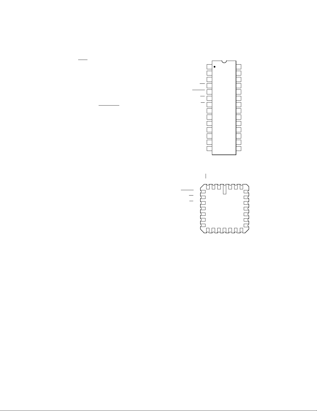
PIN CONFIGURATIONS
DIP and SOIC
LCCC
CHANNEL-TO-CHANNEL ISOLATION
Channel-to-Channel Isolation is a measure of the level of
crosstalk between channels. It is measured by applying a fullscale 1 kHz signal to the other three inputs. The figure given is
the worst case across all four channels.
SNR, THD, IMD
See DYNAMIC SPECIFICATIONS section.
–4–
REV. C
PIN FUNCTION DESCRIPTION
Pin Mnemonic Description
AD7874
1V
IN1
Analog Input Channel 1. This is the first of the four input channels to be converted in a con-
version cycle. Analog input voltage range is ± 10 V.
2V
3V
4
5
IN2
DD
INT Interrupt. Active low logic output indicating converter status. See Figure 7.
CONVST Convert Start. Logic Input. A low to high transition on this input puts the track/hold into its
Analog Input Channel 2. Analog input voltage range is ±10 V.
Positive supply voltage, +5 V ± 5%. This pin should be decoupled to AGND.
hold mode and starts conversion. The four channels are converted sequentially, Channel 1 to
Channel 4. The
6
RD Read. Active low logic input. This input is used in conjunction with CS low to enable the
CONVST input is asynchronous to CLK and independent of CS and RD.
data outputs. Four successive reads after a conversion will read the data from the four chan-
nels in the sequence, Channel 1, 2, 3, 4.
7
CS Chip Select. Active low logic input. The device is selected when this input is active.
8 CLK Clock Input. An external TTL-compatible clock may be applied to this input pin. Alterna-
9V
DD
tively, tying this pin to V
Positive Supply Voltage, +5 V ± 5%. Same as Pin 3; both pins must be tied together at the
enables the internal laser trimmed clock oscillator.
SS
package. This pin should be decoupled to DGND.
10 DB11 Data Bit 11 (MSB). Three-state TTL output. Output coding is 2s complement.
11–13 DB10–DB8 Data Bit 10 to Data Bit 8. Three-state TTL outputs.
14 DGND Digital Ground. Ground reference for digital circuitry.
15–21 DB7–DB1 Data Bit 7 to Data Bit 1. Three-state TTL outputs.
22 DB0 Data Bit 0 (LSB). Three-state TTL output.
23 AGND Analog Ground. Ground reference for track/hold, reference and DAC.
24 REF IN Voltage Reference Input. The reference voltage for the part is applied to this pin. It is inter-
nally buffered, requiring an input current of only ±1 µA. The nominal reference voltage for
correct operation of the AD7874 is 3 V.
25 REF OUT Voltage Reference Output. The internal 3 V analog reference is provided at this pin. To oper-
ate the AD7874 with internal reference, REF OUT is connected to REF IN. The external
load capability of the reference is 500 µA.
26 V
27 V
28 V
SS
IN3
IN4
Negative Supply Voltage, –5 V ± 5%.
Analog Input Channel 3. Analog input voltage range is ±10 V.
Analog Input Channel 4. Analog input voltage range is ±10 V.
REV. C
ORDERING GUIDE
Relative
Temperature SNR Accuracy Package
Range (dBs) (LSB) Option
Model
1
AD7874AN –40°C to +85°C 70 min ±1 max N-28
AD7874BN –40°C to +85°C 72 min ±1/2 max N-28
AD7874AR –40°C to +85°C 70 min ±1 max R-28
AD7874BR –40°C to +85°C 72 min ±1/2 max R-28
AD7874AQ –40°C to +85°C 70 min ±1 max Q-28
AD7874BQ –40°C to +85°C 72 min ±1/2 max Q-28
AD7874SQ
AD7874SE
NOTES
1
To order MIL-STD-883, Class B processed parts, add /883B to part number. Contact
1
our local sales office for military data sheet and availability.
2
E = Leaded Ceramic Chip Carrier; N = Plastic DIP; Q = Cerdip; R = SOIC.
3
Available to /883B processing only.
3
–55°C to +125°C 70 min ±1 max Q-28
3
–55°C to +125°C 70 min ±1 max E-28A
–5–
2
AD7874
CONVERTER DETAILS
The AD7874 is a complete 12-bit, 4-channel data acquisition
system. It is comprised of a 12-bit successive approximation
ADC, four high speed track/hold circuits, a four-channel analog
multiplexer and a 3 V Zener reference. The ADC uses a successive approximation technique and is based on a fast-settling,
voltage switching DAC, a high speed comparator, a fast CMOS
SAR and high speed logic.
Conversion is initiated on the rising edge of
CONVST. All four
input track/holds go from track to hold on this edge. Conversion
is first performed on the Channel 1 input voltage, then Channel
2 is converted and so on. The four results are stored in on-chip
registers. When all four conversions have been completed,
INT
goes low indicating that data can be read from these locations.
The conversion sequence takes either 78 or 79 rising clock edges
depending on the synchronization of
CONVST with CLK. Internal delays and reset times bring the total conversion time
from
CONVST going high to INT going low to 32.5 µs maxi-
mum for a 2.5 MHz external clock. The AD7874 uses an implicit addressing scheme whereby four successive reads to the
same memory location access the four data words sequentially.
The first read accesses Channel 1 data, the second read accesses
Channel 2 data and so on. Individual data registers cannot be
accessed independently.
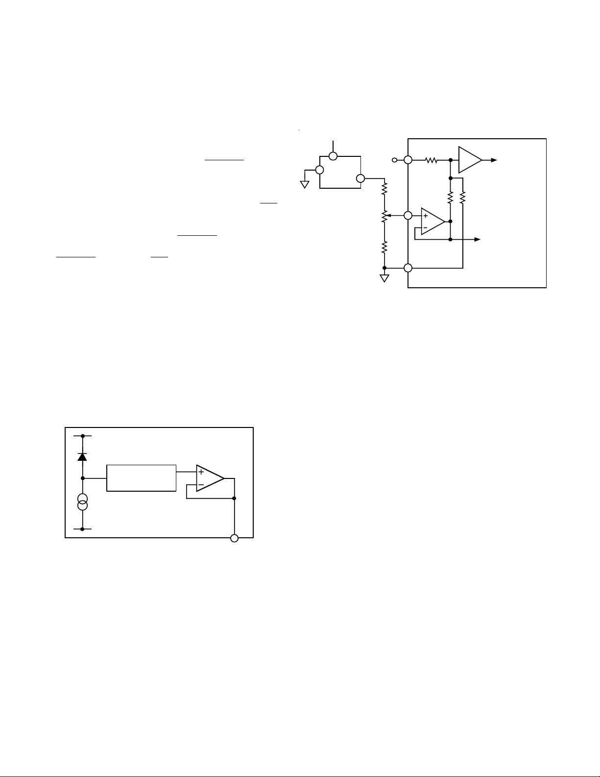
INTERNAL REFERENCE
The AD7874 has an on-chip temperature compensated buried
Zener reference which is factory trimmed to 3 V ± 10 mV (see
Figure 3). The reference voltage is provided at the REF OUT
pin. This reference can be used to provide both the reference
voltage for the ADC and the bipolar bias circuitry. This is
achieved by connecting REF OUT to REF IN.
V
DD
TEMPERATURE
COMPENSATION
V
SS
AD7874
REF OUT
Figure 3. AD7874 Internal Reference
The reference can also be used as a reference for other components and is capable of providing up to 500 µA to an external
load. In systems using several AD7874s, using the REF OUT of
one device to provide the REF IN for the other devices ensures
good full-scale tracking between all the AD7874s. Because the
AD7874 REF IN is buffered, each AD7874 presents a high impedance to the reference so one AD7874 REF OUT can drive
several AD7874 REF INs.
The maximum recommended capacitance on REF OUT for
normal operation is 50 pF. If the reference is required for other
system uses, it should be decoupled to AGND with a 200 Ω resistor in series with a parallel combination of a 10 µF tantalum
capacitor and a 0.1 µF ceramic capacitor.
EXTERNAL REFERENCE
In some applications, the user may require a system reference or
some other external reference to drive the AD7874 reference input. Figure 4 shows how the AD586 5 V reference can be used
to provide the 3 V reference required by the AD7874 REF IN.
+
15V
+V
GND
IN
V
AD586
OUT
10kΩ
1kΩ
15kΩ
V
REF
AGND
7R*
IN1
TRACK/HOLD 1
2.1R* 3R*
IN
TO ADC
REFERENCE
CIRCUITRY
*R = 3.6kΩ TYP
**ADDITIONAL PINS OMITTED FOR CLARITY
TO INTERNAL
COMPARATOR
AD7874**
Figure 4. AD586 Driving AD7874 REF IN
TRACK-AND-HOLD AMPLIFIER
The track-and-hold amplifier on each analog input of the
AD7874 allows the ADC to accurately convert an input sine
wave of 20 V p-p amplitude to 12-bit accuracy. The input bandwidth of the track/hold amplifier is greater than the Nyquist rate
of the ADC even when the ADC is operated at its maximum
throughput rate. The small signal 3 dB cutoff frequency occurs
typically at 500 kHz.
The four track/hold amplifiers sample their respective input
channels simultaneously. The aperture delay of the track/hold
circuits is small and, more importantly, is well matched across
the four track/holds on one device and also well matched from
device to device. This allows the relative phase information between different input channels to be accurately preserved. It also
allows multiple AD7874s to sample more than four channels
simultaneously.
The operation of the track/hold amplifiers is essentially transparent to the user. Once conversion is initiated, the four channels
are automatically converted and there is no need to select which
channel is to be digitized.
ANALOG INPUT
The analog input of Channel 1 of the AD7874 is as shown in
Figure 4. The analog input range is ±10 V into an input resistance of typically 30 kΩ. The designed code transitions occur
midway between successive integer LSB values (i.e., 1/2 LSB,
3/2 LSBs, 5/2 LSBs, . . . FS – 3/2 LSBs). The output code is
2s complement binary with 1 LSB = FS/4096 = 20 V/4096 =
4.88 mV. The ideal input/output transfer function is shown in
Figure 5.
–6–
REV. C

AD7874
OUTPUT
CODE
011...111
011...110
000...010
–
000...001
000...000
111...111
111...110
100...001
100...000
FS
2
+
FS
1LSB–
2
FS=20V
FS
1LSB =
4096
0V
INPUT VOLTAGE
Figure 5. Input/Output Transfer Function
OFFSET AND FULL-SCALE ADJUSTMENT
In most Digital Signal Processing (DSP) applications, offset and
full-scale errors have little or no effect on system performance.
Offset error can always be eliminated in the analog domain by
ac coupling. Full-scale error effect is linear and does not cause
problems as long as the input signal is within the full dynamic
range of the ADC. Invariably, some applications will require
that the input signal span the full analog input dynamic range.
In such applications, offset and full-scale error will have to be
adjusted to zero.
Figure 6 shows a circuit which can be used to adjust the offset
and full-scale errors on the AD7874 (Channel 1 is shown for example purposes only). Where adjustment is required, offset error must be adjusted before full-scale error. This is achieved by
trimming the offset of the op amp driving the analog input of
the AD7874 while the input voltage is a 1/2 LSB below analog
ground. The trim procedure is as follows: apply a voltage of
–2.44 mV (–1/2 LSB) at V
in Figure 6 and adjust the op amp
1
offset voltage until the ADC output code flickers between 1111
1111 1111 and 0000 0000 0000.
INPUT
RANGE = ±10V
V
1
R1
10kΩ
R2
500Ω
R4
10kΩ
R5
R3
10kΩ
10kΩ
*ADDITIONAL PINS OMITTED FOR CLARITY
V
IN1
AD7874*
AGND
Figure 6. AD7874 Full-Scale Adjust Circuit
Gain error can be adjusted at either the first code transition
(ADC negative full scale) or the last code transition (ADC positive full scale). The trim procedures for both cases are as
follows:
Positive Full-Scale Adjust
Apply a voltage of +9.9927 V (FS/2 – 3/2 LSBs) at V1. Adjust
R2 until the ADC output code flickers between 0111 1111 1110
and 0111 1111 1111.
Negative Full-Scale Adjust
Apply a voltage of –9.9976 V ( –FS + 1/2 LSB) at V1 and adjust
R2 until the ADC output code flickers between 1000 0000 0000
and 1000 0000 0001.
An alternative scheme for adjusting full-scale error in systems
which use an external reference is to adjust the voltage at the
REF IN pin until the full-scale error for any of the channels is
adjusted out. The good full-scale matching of the channels will
ensure small full-scale errors on the other channels.
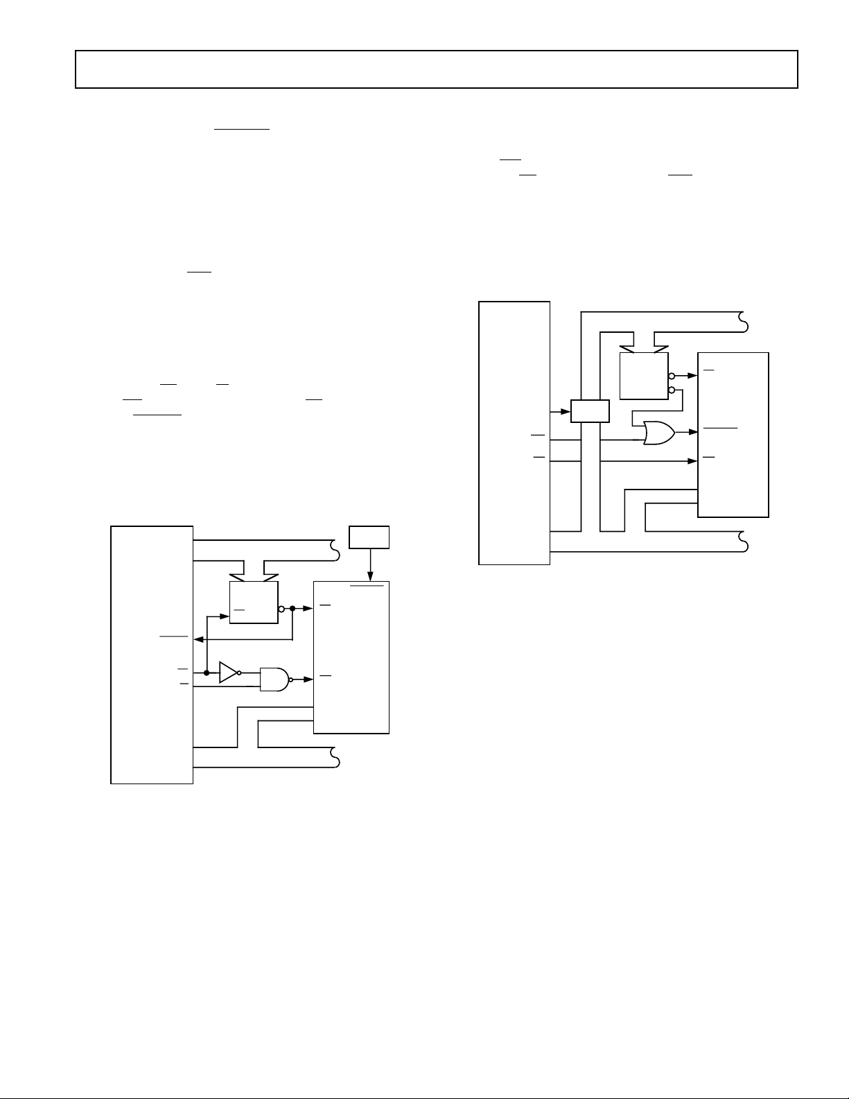
TIMING AND CONTROL
Conversion is initiated on the AD7874 by asserting the
CONVST input. This CONVST input is an asynchronous input
which is independent of the ADC clock. This is essential for
applications where precise sampling in time is important. In
these applications, the signal sampling must occur at exactly
equal intervals to minimize errors due to sampling uncertainty
or jitter. In these cases, the
CONVST input is driven from a
timer or precise clock source. Once conversion is started,
CONVST should not be asserted again until conversion is complete on all four channels.
In applications where precise time interval sampling is not critical, the
CONVST pulse can be generated from a microprocessor WRITE or READ line gated with a decoded address
(different to the AD7874
CS address). CONVST should not be
derived from a decoded address alone because very short
CONVST pulses (which may occur in some microprocessor systems as the address bus is changing at the start of an instruction
cycle) could initiate a conversion.
All four track/hold amplifiers go from track to hold on the rising
edge of the
CONVST pulse. The four track/hold amplifiers remain in their hold mode while all four channels are converted.
The rising edge of
Channel 1 input voltage (V
CONVST also initiates a conversion on the
). When conversion is complete
IN1
on Channel 1, its result is stored in Data Register 1, one of four
on-chip registers used to store the conversion results. When the
result from the first conversion is stored, conversion is initiated
on the voltage held by track/hold 2. When conversion has been
completed on the voltage held by track/hold 4 and its result is
stored in Data Register 4,
INT goes low to indicate that the
conversion process is complete.
The sequence in which the channel conversions takes place is
automatically taken care of by the AD7874. This means that the
user does not have to provide address lines to the AD7874 or
worry about selecting which channel is to be digitized.
Reading data from the device consists of four read operations to
the same microprocessor address. Addressing of the four
on-chip data registers is again automatically taken care of by the
AD7874.
REV. C
–7–

AD7874
z
The first read operation to the AD7874 after conversion always
accesses data from Data Register 1 (i.e., the conversion result
from the V
RD during this first read operation. The second read always accesses data from Data Register 2 and so on. The address pointer
is reset to point to Data Register 1 on the rising edge of
CONVST. A read operation to the AD7874 should not be attempted during conversion. The timing diagram for the
AD7874 conversion sequence is shown in Figure 7.
CONVST
INT
CS
RD
DATA
TIMES t2, t3, t4, t6, t7, AND t8 ARE THE SAME FOR ALL FOUR READ OPERATIONS.
AD7874 DYNAMIC SPECIFICATIONS
The AD7874 is specified and 100% tested for dynamic performance specifications as well as traditional dc specifications such
as Integral and Differential Nonlinearity. These ac specifications
are required for the signal processing applications such as
phased array sonar, adaptive filters and spectrum analysis.
These applications require information on the ADC’s effect on
the spectral content of the input signal. Hence, the parameters
for which the AD7874 is specified include SNR, harmonic distortion, intermodulation distortion and peak harmonics. These
terms are discussed in more detail in the following sections.
Signal-to-Noise Ratio (SNR)
SNR is the measured signal to noise ratio at the output of the
ADC. The signal is the rms magnitude of the fundamental.
Noise is the rms sum of all the nonfundamental signals up to
half the sampling frequency (fs/2) excluding dc. SNR is dependent upon the number of quantization levels used in the digitization process; the more levels, the smaller the quantization
noise. The theoretical signal to noise ratio for a sine wave input
is given by
where N is the number of bits.
Thus for an ideal 12-bit converter, SNR = 74 dB.
The output spectrum from the ADC is evaluated by applying a
sine wave signal of very low distortion to the V
sampled at a 29 kHz sampling rate. A Fast Fourier Transform
(FFT) plot is generated from which the SNR data can be obtained. Figure 8 shows a typical 2048 point FFT plot of the
AD7874BN with an input signal of 10 kHz and a sampling
frequency of 29 kHz. The SNR obtained from this graph is
73.2 dB. It should be noted that the harmonics are taken into
account when calculating the SNR.
input). INT is reset high on the falling edge of
IN1
TRACK/HOLDS GO
INTO HOLD
t
1
t
HIGH-IMPEDANCE
CONV
t
2
t
3
t
6
CH1
DATA
t
5
t
8
HIGH-
t
4
t
7
Z
t
ACQUISITION
CH2
HIGH-
DATA
CH4
HIGH-
CH3
DATA
Z
Z
DATA
HIGH-Z
Figure 7. AD7874 Timing Diagram
SNR = (6.02N + 1.76) dB (1)
input which is
IN
Figure 8. AD7874 FFT Plot
Effective Number of Bits
The formula given in Equation 1 relates the SNR to the number
of bits. Rewriting the formula, as in Equation 2, it is possible to
get a measure of performance expressed in effective number of
bits (N).
SNR −1.76
N =
6.02
(2)
The effective number of bits for a device can be calculated directly from its measured SNR.
Figure 9 shows a typical plot of effective number of bits versus
frequency for an AD7874BN with a sampling frequency of
29 kHz. The effective number of bits typically falls between
11.75 and 11.87 corresponding to SNR figures of 72.5 dB and
73.2 dB.
Figure 9. Effective Numbers of Bits vs. Frequency
–8–
REV. C

AD7874
Total Harmonic Distortion (THD)
Total Harmonic Distortion (THD) is the ratio of the rms sum
of harmonics to the rms value of the fundamental. For the
AD7874, THD is defined as
2
2
2
2
2
+V
5
6
THD = 20log
+V
+V
V
2
3
+V
4
V
1
where V1 is the rms amplitude of the fundamental and V2, V3,
V
, V5 and V6 are the rms amplitudes of the second through the
4
sixth harmonic. The THD is also derived from the FFT plot of
the ADC output spectrum.
Intermodulation Distortion
With inputs consisting of sine waves at two frequencies, fa and
fb, any active device with nonlinearities will create distortion
products at sum and difference frequencies of mfa ± nfb where
m, n = 0, 1, 2, 3 . . ., etc. Intermodulation terms are those for
which neither m or n are equal to zero. For example, the second
order terms include (fa + fb) and (fa – fb) while the third order
terms include (2fa + fb), (2fa – fb), (fa + 2fb) and (fa – 2fb).
Using the CCIF standard where two input frequencies near the
top end of the input bandwidth are used, the second and third
order terms are of different significance. The second order terms
are usually distanced in frequency from the original sine waves
while the third order terms are usually at a frequency close to
the input frequencies. As a result, the second and third order
terms are specified separately. The calculation of the intermodulation distortion is as per the THD specification where it is the
ratio of the rms sum of the individual distortion products to the
rms amplitude of the fundamental expressed in dBs. In this case,
the input consists of two, equal amplitude, low distortion sine
waves. Figure 10 shows a typical IMD plot for the AD7874.
Peak Harmonic or Spurious Noise
Harmonic or Spurious Noise is defined as the ratio of the rms
value of the next largest component in the ADC output spectrum (up to fs/2 and excluding dc) to the rms value of the fundamental. Normally, the value of this specification will be
determined by the largest harmonic in the spectrum, but for
parts where the harmonics are buried in the noise floor the peak
will be a noise peak.
AC Linearity Plot
When a sine wave of specified frequency is applied to the VIN input of the AD7874 and several million samples are taken, a histogram showing the frequency of occurrence of each of the 4096
ADC codes can be generated. From this histogram data it is
possible to generate an ac integral linearity plot as shown in Figure 11. This shows very good integral linearity performance
from the AD7874 at an input frequency of 10 kHz. The absence
of large spikes in the plot shows good differential linearity. Simplified versions of the formulae used are outlined below.
INL(i) =
(V(i) −V(o))⋅4096
V( fs)−V(o)
− i
where INL(i) is the integral linearity at code i. V(fs) and V(o) are
the estimated full-scale and offset transitions, and V(i) is the estimated transition for the i
th
code.
V(i), the estimated code transition point is derived as follows:
π⋅cum(i)
V(i)=−A⋅Cos
[]
N
where A is the peak signal amplitude, N is the number of histogram samples
i
and cum(i) =
V(n)occurrences
∑
n=o
REV. C
Figure 11. AD7874 AC INL Plot
Figure 10. AD7874 IMD Plot
–9–

AD7874
A0
A15
D15
D0
IS
EN
ADDR
DECODE
ADDRESS BUS
TIMER
DATA BUS
CONVST
CS
DB11
DB0
RD
INT
AD7874*
TMS320C25
*ADDITIONAL PINS OMITTED FOR CLARITY
INTn
R/W
STRB
MSC
READY
MICROPROCESSOR INTERFACING
The AD7874 high speed bus timing allows direct interfacing to
DSP processors as well as modern 16-bit microprocessors.
Suitable microprocessor interfaces are shown in Figures 12
through 16.
AD7874–ADSP-2100 Interface
Figure 12 shows an interface between the AD7874 and the
ADSP-2100. Conversion is initiated using a timer which allows
very accurate control of the sampling instant on all four channels. The AD7874
INT line provides an interrupt to the ADSP2100 when conversion is completed on all four channels. The
four conversion results can then be read from the AD7874 using
four successive reads to the same memory address. The following instruction reads one of the four results (this instruction is
repeated four times to read all four results in sequence):
MR0 = DM(ADC)
where MR0 is the ADSP-2100 MR0 register and
ADC is the AD7874 address.
DMA13
DMA0
ADSP-2100
(ADSP-2101/
ADSP-2102)
IRQn
DMRD (RD)
DMD15
DMD0
ADDRESS BUS
ADDR
DECODE
DMS
EN
DATA BUS
* ADDITIONAL PINS OMITTED FOR CLARITY
CS
INT
RD
DB11
DB0
TIMER
CONVST
AD7874*
TIMER
PA2
ADDRESS BUS
PA0
TMS32010
ADDR
DECODE
MEN
INT
DEN
D15
EN
DATA BUS
D0
*ADDITIONAL PINS OMITTED FOR CLARITY
CONVST
CS
AD7874*
INT
RD
DB11
DB0
Figure 13. AD7874–TMS32010 Interface
AD7874–TMS320C25 Interface
Figure 14 shows an interface between the AD7874 and the
TMS320C25. As with the two previous interfaces, conversion is
initiated with a timer and the processor is interrupted when the
conversion sequence is completed. The TMS320C25 does not
have a separate
RD output to drive the AD7874 RD input directly. This has to be generated from the processor STRB and
R/
W outputs with the addition of some logic gates. The RD sig-
nal is OR-gated with the MSC signal to provide the one WAIT
state required in the read cycle for correct interface timing.
Conversion results are read from the AD7874 using the following instruction:
IN D,ADC
where D is Data Memory address and
ADC is the AD7874 address.
Figure 12. AD7874–ADSP-2100 Interface
AD7874–ADSP-2101/ADSP-2102 Interface
The interface outlined in Figure 12 also forms the basis for an
interface between the AD7874 and the ADSP-2101/ADSP-2102.
The READ line of the ADSP-2101/ADSP-2102 is labeled
In this interface, the
programmed using the Data Memory Wait State Control Register. The instruction used to read one of the four results is as
outlined for the ADSP-2100.
AD7874–TMS32010 Interface
An interface between the AD7874 and the TMS32010 is shown
in Figure 13. Once again the conversion is initiated using an ex-
RD pulse width of the processor can be
ternal timer and the TMS32010 is interrupted when all four
conversions have been completed. The following instruction is
used to read the conversion results from the AD7874:
where D is Data Memory address and
IN D,ADC
ADC is the AD7874 address.
RD.
–10–
Figure 14. AD7874–TMS320C25 Interface
REV. C
AD7874
ALE
AD15
AD0
ADDR
DECODE
ADDRESS BUS
ADDRESS/DATA BUS
CONVST
CS
DB11
DB0
RD
AD7874*
8086
*ADDITIONAL PINS OMITTED FOR CLARITY
WR
RD
LATCH
Some applications may require that the conversion is initiated
by the microprocessor rather than an external timer. One option
is to decode the AD7874
CONVST from the address bus so
that a write operation starts a conversion. Data is read at the
end of the conversion sequence as before. Figure 16 shows an
example of initiating conversion using this method. Note that
for all interfaces, a read operation should not be attempted during conversion.
AD7874–MC68000 Interface
An interface between the AD7874 and the MC68000 is shown
in Figure 15. As before, conversion is initiated using an external
timer. The AD7874
INT line can be used to interrupt the processor or, alternatively, software delays can ensure that conversion has been completed before a read to the AD7874 is
attempted. Because of the nature of its interrupts, the 68000
requires additional logic (not shown in Figure 15) to allow it to
be interrupted correctly. For further information on 68000 interrupts, consult the 68000 users manual.
The MC68000
separate
the 68000
AS and R/W outputs are used to generate a
RD input signal for the AD7874. CS is used to drive
DTACK input to allow the processor to execute a
normal read operation to the AD7874. The conversion results
are read using the following 68000 instruction:
MOVE.W ADC,D0
where D0 is the 68000 D0 register and
ADC is the AD7874 address.
AD7874–8086 Interface
Figure 16 shows an interface between the AD7874 and the 8086
microprocessor. Unlike the previous interface examples, the
microprocessor initiates conversion. This is achieved by gating
the 8086
the AD7874
WR signal with a decoded address output (different to
CS address). The AD7874 INT line is used to in-
terrupt the microprocessor when the conversion sequence is
completed. Data is read from the AD7874 using the following
instruction:
MOV AX,ADC
where AX is the 8086 accumulator and
ADC is the AD7874 address.
A15
A0
MC68000
DTACK
AS
R/W
D15
D0
ADDRESS BUS
ADDR
DECODE
EN
DATA BUS
*ADDITIONAL PINS OMITTED FOR CLARITY
Figure 15. AD7874–MC68000 Interface
CS
AD7874*
RD
DB11
DB0
TIMER
CONVST
Figure 16. AD7874–8086 Interface
REV. C
–11–

AD7874
APPLICATIONS
Vector Motor Control
The current drawn by a motor can be split into two components: one produces torque and the other produces magnetic
flux. For optimal performance of the motor, these two components should be controlled independently. In conventional
methods of controlling a three-phase motor, the current (or
voltage) supplied to the motor and the frequency of the drive are
the basic control variables. However, both the torque and flux
are functions of current (or voltage) and frequency. This coupling effect can reduce the performance of the motor because,
for example, if the torque is increased by increasing the frequency, the flux tends to decrease.
Vector control of an ac motor involves controlling phase in addition to drive and current frequency. Controlling the phase of the
motor requires feedback information on the position of the rotor
relative to the rotating magnetic field in the motor. Using this
information, a vector controller mathematically transforms the
three phase drive currents into separate torque and flux components. The AD7874, with its four-channel simultaneous sampling capability, is ideally suited for use in vector motor control
applications.
DSP
MICROPROCESSOR
TORQUE & FLUX
CONTROL LOOP
CALCULATIONS &
TWO TO THREE
PHASE
INFORMATION
DAC
DAC
DAC
A block diagram of a vector motor control application using the
AD7874 is shown in Figure 17. The position of the field is derived by determining the current in each phase of the motor.
Only two phase currents need to be measured because the third
can be calculated if two phases are known. Channel 1 and
Channel 2 of the AD7874 are used to digitize this information.
Simultaneous sampling is critical to maintain the relative phase
information between the two channels. A current sensing isolation amplifier, transformer or Hall effect sensor is used between
the motor and the AD7874. Rotor information is obtained by
measuring the voltage from two of the inputs to the motor.
Channel 3 and Channel 4 of the AD7874 are used to obtain this
information. Once again the relative phase of the two channels
is important. A DSP microprocessor is used to perform the
mathematical transformations and control loop calculations on
the information fed back by the AD7874.
I
C
DRIVE
CIRCUITRY
I
B
I
A
V
3
B
PHASE
MOTOR
V
A
TORQUE
SETPOINT
FLUX
SETPOINT
TRANSFORMATION
TO TORQUE &
FLUX CURRENT
COMPONENTS
*ADDITIONAL PINS OMITTED FOR CLARITY
AD7874*
V
IN1
V
IN2
V
IN3
V
IN4
ISOLATION
AMPLIFIERS
ATTENUATORS
Figure 17. Vector Motor Control Using the AD7874
VOLTAGE
–12–
REV. C

AD7874
MULTIPLE AD7874s
Figure 18 shows a system where a number of AD7874s can be
configured to handle multiple input channels. This type of configuration is common in applications such as sonar, radar, etc.
The AD7874 is specified with maximum and minimum limits on
aperture delay. This means that the user knows the maximum
difference in the sampling instant between all channels. This allows the user to maintain relative phase information between the
different channels.
A common read signal from the microprocessor drives the
RD
input of all AD7874s. Each AD7874 is designated a unique address selected by the address decoder. The reference output of
AD7874 number 1 is used to drive the reference input of all
other AD7874s in the circuit shown in Figure 18. One REF
OUT pin can drive several AD7874 REF IN pins. Alternatively,
an external or system reference can be used to drive all REF IN
inputs. A common reference ensures good full-scale tracking between all channels.
V
CH1
V
V
V
V
CH2
V
CH3
V
CH4
V
CH5
V
CH6
V
CH7
V
CH8
V
CHm
CHm+1
CHm+2
CHm+3
RD
AD7874(1)
CS
REF OUT
RD
AD7874(2)
CS
REF IN
REF IN
RD
AD7874(n)
CS
ADDRESS
DECODE
RD
ADDRESS
the input signal connects to the buffer amplifier driving the analog input of the ADC. If the shorting plug is omitted, a wire link
can be used to connect the input signal to the PCB component
grid.
Microprocessor connections to the board are made via a 26contact IDC connector, SKT8, the pinout for which is shown in
Figure 19. This connector contains all data, control and status
signals of the AD7874 (with the exception of the CLK input
and the
SKT7, respectively). It also contains decoded R/
CONVST input which are provided via SKT5 and
W and STRB
inputs which are necessary for TMS32020 interfacing (and also
for 68000 interfacing although pin labels on the 68000 are different). Note that the AD7874
CS input must be decoded prior
to the AD7874 evaluation board.
SKT1, SKT2, SKT3 and SKT4 provide the inputs for V
V
, V
, V
IN2
IN3
respectively. Assuming LK1 to LK4 are in
IN4
IN1
,
place, these input signals are fed to four buffer amplifiers, IC1,
before being applied to the AD7874. The use of an external
clock source is optional; there is a shorting plug (LK5) on the
AD7874 CLK input which must be connected to either –5 V
(for the ADCs own internal clock) or to SKT5. SKT6 and
SKT7 provide the reference and
CONVST inputs respectively.
Shorting plug LK6 provides the option of using the external reference or the ADCs own internal reference.
1
2
R/W
N/C
N/C
DB10
DB8
DB6
DB4
DB2
DB0
+
GND
RD
CS
3
5
7
9
11
13
15
17
19
21
23
5V
25
STRB
4
N/C
6
N/C
8
INT
10
N/C
12
DB11
14
DB9
16
DB7
18
DB5
20
DB3
22
DB1
24
+
5V
26
GND
Figure 18. Multiple AD7874s in Multichannel System
DATA ACQUISITION BOARD
Figure 20 shows the AD7874 in a data acquisition circuit. The
corresponding printed circuit board (PCB) layout and silkscreen
are shown in Figures 21 to 23. A 26-contact IDC connector provides for a microprocessor connection to the board.
A component grid is provided near the analog inputs on the
PCB which may be used to provide antialiasing filters for the
analog input channels or to provide signal conditioning circuitry.
To facilitate this option, four shorting plugs (labeled LK1 to
LK4 on the PCB) are provided on the analog inputs, one plug
per input. If the shorting plug for a particular channel is used,
REV. C
–13–
Figure 19. SKT8, IDC Connector Pinout
POWER SUPPLY CONNECTIONS
The PCB requires two analog power supplies and one 5 V digital supply. The analog supplies are labeled V+ and V– and the
range for both supplies is 12 V to 15 V (see silkscreen in Figure
23). Connection to the 5 V digital supply is made via SKT8.
The +5 V supply and the –5 V supply required by the AD7874
are generated from voltage regulators (IC3 and IC4) on the V+
and V– supplies.

AD7874
SKT1
SKT2
SKT3
SKT4
C4
C2
78L05
V
DD
IN
IC3
IC1
AD713
79L05
IC4
C7
V
IN1
V
IN2
V
IN3
V
IN4
AGND
DGND
OUT
C5
C8
V
DD
CONVST
DB11
DB0
INT
IC2
AD7874
REF IN
REF
OUT
V
CLK
SS
C6
CONVST
SKT6
CS
RD
LK5
AB
CLK
SKT5
DATA BUS
A
IC5
B
A
B
REFERENCE
SKT6
IC5
+
5V
R1R2
DGND
SKT8
11
22
8
5
23, 24
2
1
3
25, 26
+
V
C3
LK1
LK2
LK3
LK4
V
SS
C1
V–
Figure 20. Data Acquisition Circuit Using the AD7874
Figure 21. PCB Silkscreen for Figure 20
–14–
REV. C
AD7874
Figure 22. PCB Component Side Layout for the Circuit of Figure 20
REV. C
Figure 23. PCB Solder Side Layout for the Circuit of Figure 20
–15–

AD7874
SHORTING PLUG OPTIONS
There are seven shorting plug options which must be set before
using the board. These are outlined below:
LK1–LK4 Connects the analog inputs to the buffer amplifi-
ers. The analog inputs may also be connected to a
component grid for signal conditioning.
LK5 Selects either the AD7874 internal clock or an ex-
ternal clock source.
LK6 Selects either the AD7874 internal reference or an
external reference source.
LK7 Connects the AD7874
RD input directly to the
RD input of SKT8 or to a decoded STRB and
R/
W input. This shorting plug setting depends on
the microprocessor, e.g., the TMS32020 and
68000 require a decoded
RD signal.
OUTLINE DIMENSIONS
Dimensions shown in inches and (mm).
Plastic (N-28)
COMPONENT LIST
IC1 AD713 Quad Op Amp
IC2 AD7874 Analog-to-Digital Converter
IC3 MC78L05 +5 V Regulator
IC4 MC79L05 –5 V Regulator
IC5 74HC00 Quad NAND Gate
C1, C3, C5, C7, C9 10 µF Capacitors
C2, C4, C6, C8, C10 0.1 µF Capacitors
R1, R2 10 kΩ Pull-Up Resistors
LK1, LK2, LK3 Shorting Plugs
LK4, LK5, LK6
LK7
SKT1, SKT2, SKT3, BNC Sockets
SKT4, SKT5, SKT6,
SKT7
SKT8 26-Contact (2-Row) IDC Connector
SOIC (R-28)
C1388a–5–5/91
Cerdip (Q-28)
–16–
0.100 (2.54)
0.064 (1.63)
1
0.050 ± 0.005
(1.27 ± 0.13)
0.040 x 45°
(1.02 x 45°)
REF 3 PLCS
0.055 (1.40)
0.045 (1.14)
LCCC (E-28A)
0.075
(1.91)
REF
0.028 (0.71)
0.022 (0.56)
28
NO. 1 PIN INDEX
BOTTOM VIEW
0.020 x 45°
0.458 (11.63)
NOTES
1. THIS DIMENSION CONTROLS THE OVERALL PACKAGE
THICKNESS.
2. APPLIES TO ALL FOUR SIDES.
3. ALL TERMINALS ARE GOLD PLATED.
0.442 (11.23)
2
(0.51 x 45°) REF
PRINTED IN U.S.A.
REV. C
 Loading...