Analog Devices AD7818, AD7817, AD7816 Datasheet

REV. A
Information furnished by Analog Devices is believed to be accurate and
reliable. However, no responsibility is assumed by Analog Devices for its
use, nor for any infringements of patents or other rights of third parties
which may result from its use. No license is granted by implication or
otherwise under any patent or patent rights of Analog Devices.
a
AD7816/AD7817/AD7818
One Technology Way, P.O. Box 9106, Norwood, MA 02062-9106, U.S.A.
Tel: 781/329-4700 World Wide Web Site: http://www.analog.com
Fax: 781/326-8703 © Analog Devices, Inc., 2000
Single- and 4-Channel, 9 s, 10-Bit ADCs
with On-Chip Temperature Sensor
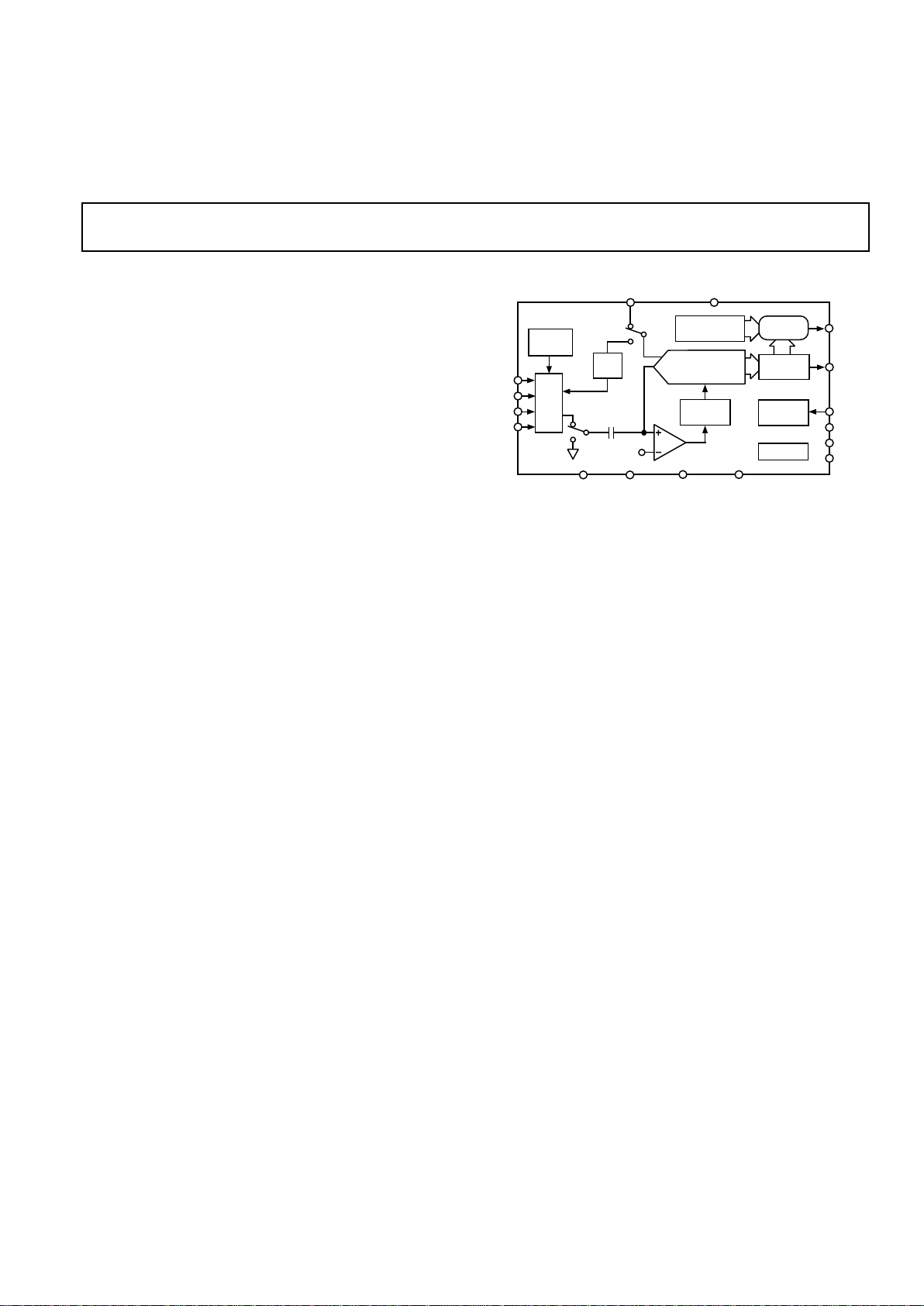
FUNCTIONAL BLOCK DIAGRAM
FEATURES
10-Bit ADC with 9 s Conversion Time
One (AD7818) and Four (AD7817) Single-Ended Analog
Input Channels
The AD7816 Is a Temperature Measurement Only Device
On-Chip Temperature Sensor
Resolution of 0.25ⴗC
ⴞ2ⴗC Error from –40ⴗC to +85ⴗC
–55ⴗC to +125ⴗC Operating Range
Wide Operating Supply Range
+2.7 V to +5.5 V
Inherent Track-and-Hold Functionality
On-Chip Reference (2.5 V ⴞ 1%)
Over-Temperature Indicator
Automatic Power-Down at the End of a Conversion
Low Power Operation
4 W at a Throughput Rate of 10 SPS
40 W at a Throughput Rate of 1 kSPS
400 W at a Throughput Rate of 10 kSPS
Flexible Serial Interface
APPLICATIONS
Ambient Temperature Monitoring (AD7816)
Thermostat and Fan Control
High Speed Microprocessor
Temperature Measurement and Control
Data Acquisition Systems with Ambient Temperature
Monitoring (AD7817 and AD7818)
Industrial Process Control
Automotive
Battery Charging Applications
GENERAL DESCRIPTION
The AD7818 and AD7817 are 10-bit, single- and 4-channel
A/D converters with on-chip temperature sensor that can operate from a single 2.7 V to 5.5 V power supply. Each part con-
tains a 9 µs successive-approximation converter based around
a capacitor DAC, an on-chip temperature sensor with an accu-
racy of ±2°C, an on-chip clock oscillator, inherent track-and-
hold functionality and an on-chip reference (2.5 V). The
AD7816 is a temperature monitoring only device in a SOIC/
µSOIC package.
The on-chip temperature sensor of the AD7817 and AD7818
can be accessed via Channel 0. When Channel 0 is selected and
a conversion is initiated, the resulting ADC code at the end of
the conversion gives a measurement of the ambient temperature
with a resolution of ±0.25°C. See Measuring Temperature section
of the data sheet.
The AD7816, AD7817 and AD7818 have a flexible serial interface that allows easy interfacing to most microcontrollers.
The interface is compatible with the Intel 8051, Motorola
SPI™ and QSPI™ protocols and National Semiconductors
MICROWIRE™ protocol. For more information refer to the
Serial Interface section of this data sheet.
The AD7817 is available in a narrow body 0.15" 16-lead Small
Outline IC (SOIC), in a 16-lead, Thin Shrink Small Outline
Package (TSSOP), while the AD7816/AD7818 come in an
8-lead Small Outline IC (SOIC) and an 8-lead microsmall
Outline IC (µSOIC).
PRODUCT HIGHLIGHTS
1. The devices have an on-chip temperature sensor that allows an
accurate measurement of the ambient temperature to be
made. The measurable temperature range is –55°C to +125°C.
2. An over-temperature indicator is implemented by carrying
out a digital comparison of the ADC code for Channel 0
(temperature sensor) with the contents of the on-chip overtemperature register. The over-temperature indicator pin goes
logic low when a predetermined temperature is exceeded.
3. The automatic power-down feature enables the AD7816,
AD7817 and AD7818 to achieve superior power perfor-
mance at slower throughput rates, e.g., 40 µW at 1 kSPS
throughput rate.
SPI and QSPI are trademarks of Motorola, Inc.
MICROWIRE is a trademark of National Semiconductor Corporation.
CHARGE
REDISTRIBUTION
DAC
CLOCK
D
OUT
SCLK
RD/WR
CONVST
AGND
CONTROL
REG
A
B
OVER-TEMP
REG
A > B
OTI
CONTROL
LOGIC
V
BALANCE
SAMPLING
CAPACITOR
MUX
REF
2.5V
TEMP
SENSOR
REF
IN
V
DD
DATA
OUT
D
IN
DGND
BUSY
CS
V
IN1
V
IN2
V
IN3
V
IN4
AD7817

–2– REV. A
AD7816/AD7817/AD7818
Parameter A Version *B Version *S Version Units Test Conditions/Comments
DYNAMIC PERFORMANCE Sample Rate = 100 kSPS, Any
Channel, f
IN
= 20 kHz
Signal to (Noise + Distortion) Ratio
2
58 58 58 dB min
Total Harmonic Distortion
2
–65 –65 –65 dB max –75 dB typ
Peak Harmonic or Spurious Noise
2
–65 –65 –65 dB max –75 dB typ
Intermodulation Distortion
2
fa =19.9␣ kHz, fb = 20.1␣ kHz
Second Order Terms –67 –67 –67 dB typ
Third Order Terms –67 –67 –67 dB typ
Channel-to-Channel Isolation
2
–80 –80 –80 dB typ fIN = 20 kHz
DC ACCURACY Any Channel
Resolution 10 10 10 Bits
Minimum Resolution for Which
No Missing Codes Are Guaranteed 10 10 10 Bits
Relative Accuracy
2
±1 ±1 ±1 LSB max
Differential Nonlinearity
2
±1 ±1 ±1 LSB max
Gain Error
2
±2 ±2 ±2 LSB max External Reference
±10 ±10 +20/–10 LSB max Internal Reference
Gain Error Match
2
±1/2 ±1/2 ±1/2 LSB max
Offset Error
2
±2 ±2 ±2 LSB max
Offset Error Match ±1/2 ±1/2 ±1/2 LSB max
TEMPERATURE SENSOR
1
Measurement Error External Reference V
REF
= 2.5 V
Ambient Temperature +25°C ±2 ±1 ±2 °C max
T
MIN
to T
MAX
±3 ±2 ±3 °C max
Measurement Error On-Chip Reference
Ambient Temperature +25°C ±2.25 ±2.25 ±2.25 °C max
T
MIN
to T
MAX
±3 ±3 ±6 °C max
Temperature Resolution 1/4 1/4 1/4 °C/LSB
REFERENCE INPUT
3, 4
REFIN Input Voltage Range
3
2.625 2.625 2.625 V max 2.5 V + 5%
2.375 2.375 2.375 V min 2.5 V – 5%
Input Impedance 40 40 40 kΩ min
Input Capacitance 10 10 10 pF max
ON-CHIP REFERENCE
5
Nominal 2.5 V
Temperature Coefficient
3
80 80 150 ppm/°C typ
CONVERSION RATE
Track/Hold Acquisition Time
4
400 400 400 ns max Source Impedance < 10 Ω
Conversion Time
Temperature Sensor 27 27 27 µs max
Channels 1 to 4 9 9 9 µs max
POWER REQUIREMENTS
V
DD
+5.5 +5.5 +5.5 V max For Specified Performance
+2.7 +2.7 +2.7 V min
I
DD
Logic Inputs = 0 V or V
DD
Normal Operation 2 2 2 mA max 1.6 mA typ
Using External Reference 1.75 1.75 1.75 mA max 2.5 V External Reference Connected
Power-Down 1 1 2 µA max 50 nA typ
Auto Power-Down Mode V
DD
= 3 V
10 SPS Throughput Rate 6 6 6 µW typ See Power vs. Throughput Section
1 kSPS Throughput Rate 60 60 60 µW typ for Description of Power Dissipation
10 kSPS Throughput Rate 600 600 600 µW typ in Auto Power-Down Mode
Power-Down 3 3 6 µW max Typically 0.15 µW
AD7817–SPECIFICATIONS
1
(VDD = +2.7 V to +5.5 V, GND = 0␣ V, REFIN = +2.5␣ V unless otherwise noted)

–3–REV. A
AD7816/AD78186–SPECIFICATIONS
1
(VDD = +2.7 V to +5.5 V, GND = 0 V, REFIN = +2.5 V unless
otherwise noted)
Parameter A Version Units Test Conditions/Comments
DYNAMIC PERFORMANCE (AD7818 Only) Sample Rate = 100 kSPS, Any
Channel, f
IN
= 20 kHz
Signal to (Noise + Distortion) Ratio
2
57 dB min
Total Harmonic Distortion
2
–65 dB max –75 dB typ
Peak Harmonic or Spurious Noise
2
–67 dB typ –75 dB typ
Intermodulation Distortion
2
fa = 19.9␣ kHz, fb = 20.1␣ kHz
Second Order Terms –67 dB typ
Third Order Terms –67 dB typ
Channel-to-Channel Isolation
2
–80 dB typ fIN = 20 kHz
DC ACCURACY (AD7818 Only) Any Channel
Resolution 10 Bits
Minimum Resolution for Which
No Missing Codes Are Guaranteed 10 Bits
Relative Accuracy
2
±1LSB max
Differential Nonlinearity
2
±1LSB max
Gain Error
2
±10 LSB max
Offset Error
2
±4LSB max
TEMPERATURE SENSOR
1
Measurement Error External Reference V
REF
= 2.5 V
Ambient Temperature +25°C ±2 °C max
T
MIN
to T
MAX
±3 °C max
Measurement Error On-Chip Reference
Ambient Temperature +25°C ±2 °C max
T
MIN
to T
MAX
±3 °C max
Temperature Resolution 1/4 °C/LSB
REFERENCE INPUT
3, 4
(AD7816 Only)
REF
IN
Input Voltage Range
3
2.625 V max 2.5 V + 5%
2.375 V min 2.5 V – 5%
Input Impedance 50 kΩ min
Input Capacitance 10 pF max
ON-CHIP REFERENCE
5
Nominal 2.5 V
Temperature Coefficient
3
30 ppm/°C typ
CONVERSION RATE
Track/Hold Acquisition Time
4
400 ns max Source Impedance < 10 Ω
Conversion Time
Temperature Sensor 27 µs max
Channel 1 9 µs max (AD7818 Only)
POWER REQUIREMENTS
V
DD
+5.5 V max For Specified Performance
+2.7 V min
I
DD
Logic Inputs = 0 V or V
DD
Normal Operation 2 mA max 1.3 mA typ
Using External Reference 1.75 mA max 2.5 V External Reference Connected
Power-Down 2 µA max 500 nA typ
Auto Power-Down Mode V
DD
= 3 V
10 SPS Throughput Rate 4 µW typ See Power vs. Throughput Section for
1 kSPS Throughput Rate 40 µW typ Description of Power Dissipation in
10 kSPS Throughput Rate 400 µW typ Auto Power-Down Mode
Power-Down 3 µW max Typically 0.15 µW
AD7816/AD7817/AD7818

–4–
Parameter A Version *B Version *S Version Units Test Conditions/Comments
ANALOG INPUTS
7
(AD7817 and AD7818)
Input Voltage Range V
REF
V
REF
V
REF
V max
000V min
Input Leakage ±1 ±1 ±1 µA min
Input Capacitance 10 10 10 pF max
LOGIC INPUTS
4
Input High Voltage, V
INH
2.4 2.4 2.4 V min V
DD
= 5 V ± 10%
Input Low Voltage, V
INL
0.8 0.8 0.8 V max V
DD
= 5 V ± 10%
Input High Voltage, V
INH
222V minV
DD
= 3 V ± 10%
Input Low Voltage, V
INL
0.4 0.4 0.4 V max V
DD
= 3 V ± 10%
Input Current, I
IN
±3 ±3 ±3 µA max Typically 10 nA, V
IN
= 0 V to V
DD
Input Capacitance, C
IN
10 10 10 pF max
LOGIC OUTPUTS
4
Output High Voltage, V
OH
I
SOURCE
= 200␣ µA
444V minV
DD
= 5 V ± 10%
2.4 2.4 2.4 V min V
DD
= 3 V ± 10%
Output Low Voltage, V
OL
I
SINK
= 200 µA
0.4 0.4 0.4 V max V
DD
= 5 V ± 10%
0.2 0.2 0.2 V max V
DD
= 3 V ± 10%
High Impedance Leakage Current ±1 ±1 ±1 µA max
High Impedance Capacitance 15 15 15 pF max
NOTES
*B and S Versions apply to AD7817 only. For operating temperature ranges, see Ordering Guide.
1
AD7816 and AD7817 temperature sensors specified with external +2.5 V reference, AD7818 specified with on-chip reference. All other specifications with external
and on-chip reference (+2.5 V). For VDD = +2.7 V, T
A
= +85°C max and temperature sensor measurement error = ±3°C.
2
See Terminology.
3
The accuracy of the temperature sensor is affected by reference tolerance. The relationship between the two is explained in the section titled Temperature Measurement Error Due to Reference Error.
4
Sample tested during initial release and after any redesign or process change that may affect this parameter.
5
On-chip reference shuts down when external reference is applied.
6
All specifications are typical for AD7818 at temperatures above +85°C and with V
DD
greater than +3.6 V.
7
Refers to the input current when the part is not converting. Primarily due to reverse leakage current in the ESD protection diodes.
Specifications subject to change without notice.
CHARGE
REDISTRIBUTION
DAC
CLOCK
DATA
OUT
D
IN/
OUT
SCLK
RD/WR
CONVST
AGND
CONTROL
REG
A
B
OVER-TEMP
REG
A > B
OTI
CONTROL
LOGIC
V
BALANCE
SAMPLING
CAPACITOR
MUX
REF
2.5V
TEMP
SENSOR
REF
IN
V
DD
AD7816
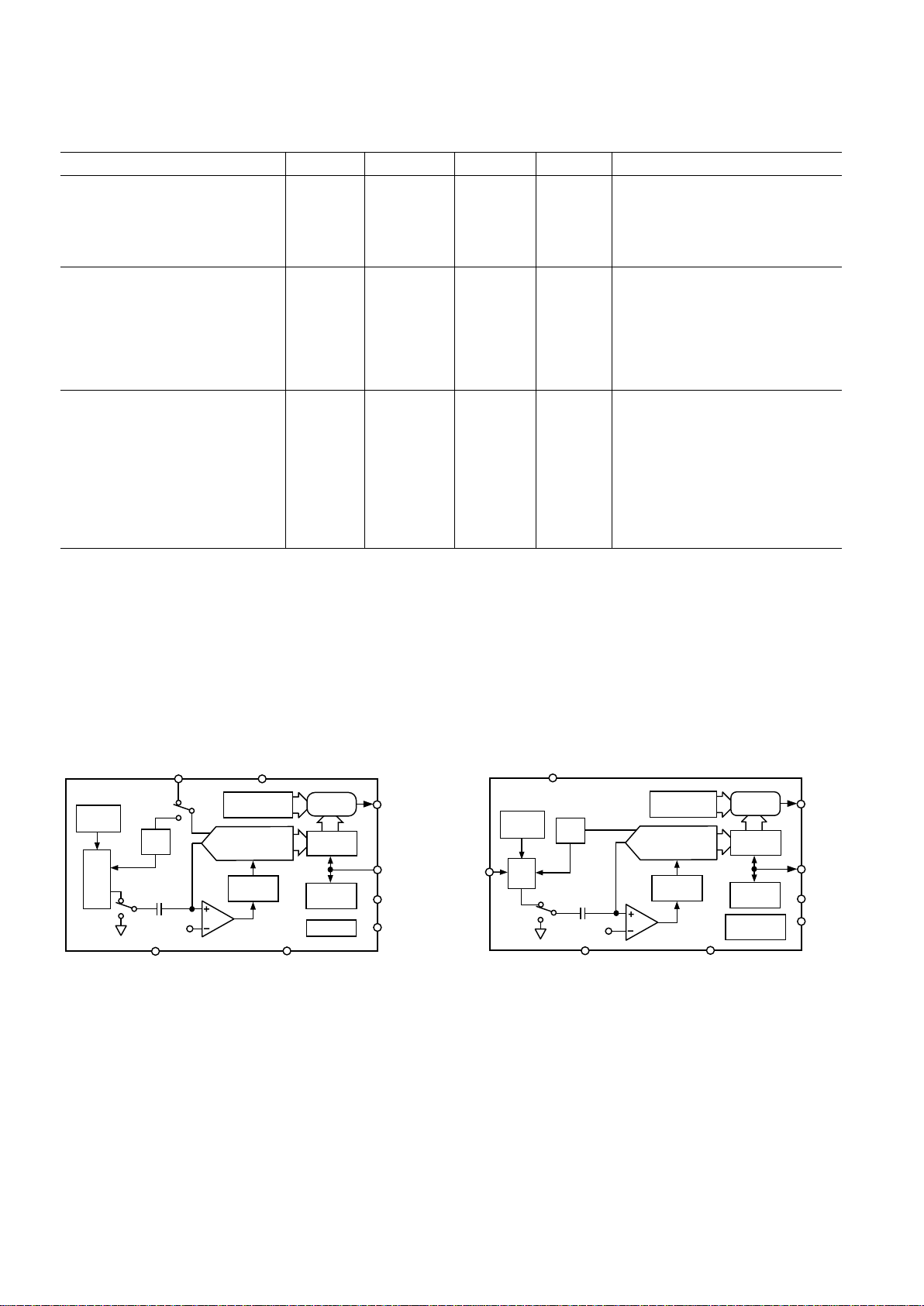
Figure 1. AD7816 Functional Block Diagram
CHARGE
REDISTRIBUTION
DAC
CLOCK
GENERATOR
DATA
OUT
D
IN/
OUT
SCLK
RD/WR
CONVST
AGND
CONTROL
REG
A
B
OVER-TEMP
REG
A > B
OTI
CONTROL
LOGIC
V
BALANCE
SAMPLING
CAPACITOR
MUX
REF
2.5V
TEMP
SENSOR
V
DD
V
IN1
AD7818
Figure 2. AD7818 Functional Block Diagram
AD7816/AD7817/AD7818–SPECIFICATIONS
1
REV. A

AD7816/AD7817/AD7818
–5–REV. A
TIMING CHARACTERISTICS
1, 2
Parameter A, B Versions Units Test Conditions/Comments
t
POWER-UP
2 µs max Power-Up Time from Rising Edge of CONVST
t
1a
9 µs max Conversion Time Channels 1 to 4
t
1b
27 µs max Conversion Time Temperature Sensor
t
2
20 ns min CONVST Pulsewidth
t
3
50 ns max CONVST Falling Edge to BUSY Rising Edge
t
4
0 ns min CS Falling Edge to RD/WR Falling Edge Setup Time
t
5
0 ns min RD/WR Falling Edge to SCLK Falling Edge Setup
t
6
10 ns min DIN Setup Time before SCLK Rising Edge
t
7
10 ns min DIN Hold Time after SCLK Rising Edge
t
8
40 ns min SCLK Low Pulsewidth
t
9
40 ns min SCLK High Pulsewidth
t
10
0 ns min CS Falling Edge to RD/WR Rising Edge Setup Time
t
11
0 ns min RD/WR Rising Edge to SCLK Falling Edge Setup Time
t
12
3
20 ns max D
OUT
Access Time after RD/WR Rising Edge
t
13
3
20 ns max D
OUT
Access Time after SCLK Falling Edge
t
14a
3, 4
30 ns max D
OUT
Bus Relinquish Time after Falling Edge of RD/WR
t
14b
3, 4
30 ns max D
OUT
Bus Relinquish Time after Rising Edge of CS
t
15
150 ns max BUSY Falling Edge to OTI Falling Edge
t
16
40 ns min RD/WR Rising Edge to OTI Rising Edge
t
17
400 ns min SCLK Rising Edge to CONVST Falling Edge (Acquisition Time of T/H)
NOTES
1
Sample tested during initial release and after any redesign or process change that may affect this parameter. All input signals are measured with tr = tf = 1␣ ns (10% to
90% of +5 V) and timed from a voltage level of +1.6␣ V.
2
See Figures 16, 17, 20 and 21.
3
These figures are measured with the load circuit of Figure 3. They are defined as the time required for D
OUT
to cross 0.8 V or 2.4 V for V
DD
= 5 V ± 10% and 0.4 V
or 2 V for V
DD
= 3 V ± 10%, as quoted on the specifications page of this data sheet.
4
These times are derived from the measured time taken by the data outputs to change 0.5␣ V when loaded with the circuit of Figure 3. The measured number is then
extrapolated back to remove the effects of charging or discharging the 50 pF capacitor. This means that the times quoted in the timing characteristics are the true bus
relinquish times of the part and as such are independent of external bus loading capacitances.
Specifications subject to change without notice.
1.6V
I
OL
200mA
200mA
I
OL
TO
OUTPUT
PIN
C
L
50pF
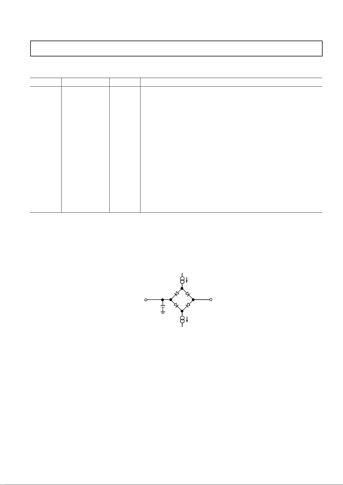
Figure 3. Load Circuit for Access Time and Bus Relinquish Time
(VDD = +2.7 V to +5.5 V, GND = 0␣ V, REFIN = +2.5␣ V. All specifications T
MIN
to T
MAX
unless
otherwise noted)
 Loading...