Analog Devices AD7810YRM, AD7810YR, AD7810YN Datasheet

2.7 V to 5.5 V, 2.3 s, 10-Bit
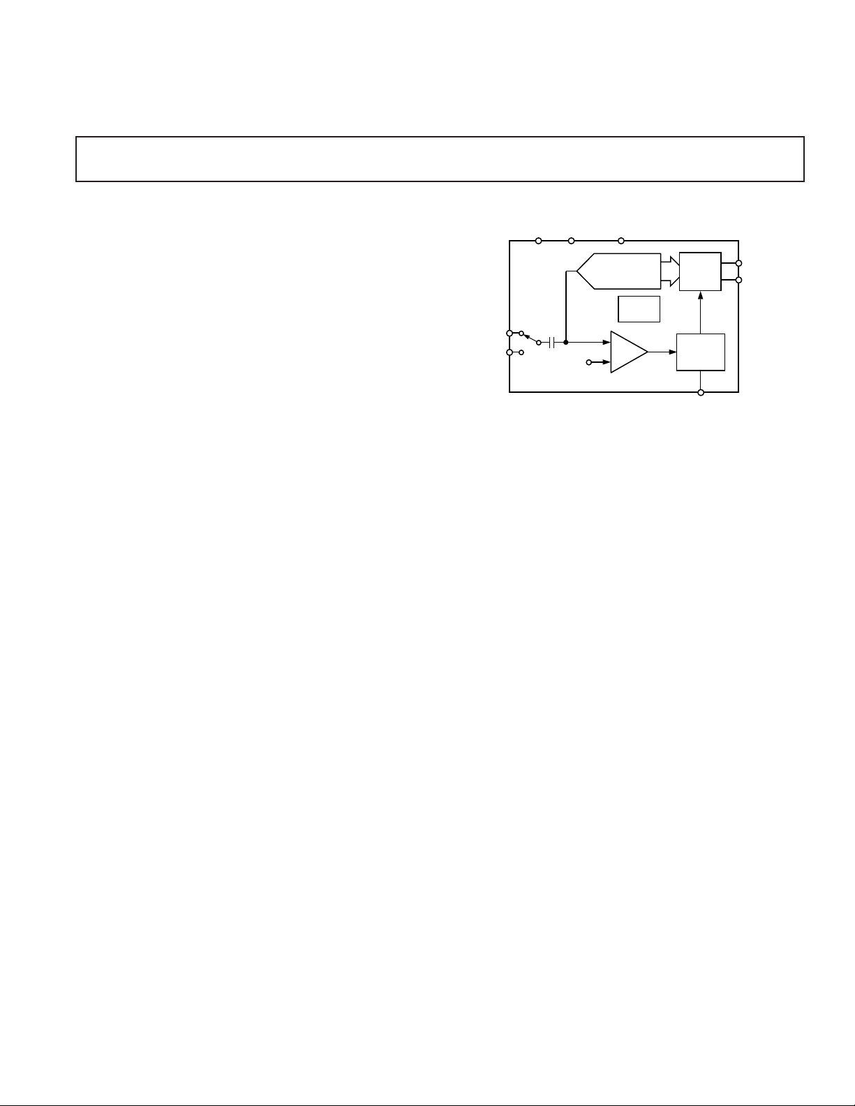
CLOCK
OSC
D
OUT
SCLK
V
REF
AGND
V
DD
VIN+
V
IN
–
CONVST
SERIAL
PORT
CHARGE
REDISTRIBUTION
DAC
CONTROL
LOGIC
AD7810
COMP
VDD/
3
a
FEATURES
10-Bit ADC with 2.3 s Conversion Time
Small Footprint 8-Lead microSOIC Package
Specified Over a –40ⴗC to +105ⴗC Temperature Range
Inherent Track-and-Hold Functionality
Operating Supply Range: 2.7 V to 5.5 V
Specifications at 2.7 V to 5.5 V
Microcontroller-Compatible Serial Interface
Optional Automatic Power-Down
at End of Conversion
Low Power Operation
270 W at 10 kSPS Throughput Rate
2.7 mW at 100 kSPS Throughput Rate
Analog Input Range: 0 V to V
Reference Input Range: 0 V to V
APPLICATIONS
Low Power, Hand-Held Portable Applications that
Require Analog-to-Digital Conversion with 10-Bit
Accuracy; e.g., Battery Powered Test Equipment,
Battery-Powered Communications Systems
REF
DD
ADC in 8-Lead microSOIC/DIP
AD7810
FUNCTIONAL BLOCK DIAGRAM
GENERAL DESCRIPTION
The AD7810 is a high speed, low power, 10-bit A/D converter that operates from a single 2.7 V to 5.5 V supply. The
part contains a 2.3 µs successive approximation A/D converter,
with inherent track/hold functionality, a pseudo differential
input and a high speed serial interface that interfaces to most
microcontrollers. The AD7810 is fully specified over a temperature range of –40°C to +105°C.
By using a technique that samples the state of the CONVST
(convert start) signal at the end of a conversion, the AD7810
may be used in an automatic power-down mode. When used in
this mode, the AD7810 automatically powers down at the end
of a conversion and “wakes up” at the start of a new conversion.
This feature significantly reduces the power consumption of the
part at lower throughput rates. The AD7810 can also operate in
a high speed mode where the part is not powered down between
conversions. In this high speed mode of operation, the conversion time of the AD7810 is 2.3 µs. The maximum throughput
rate is dependent on the speed of the serial interface of the
microcontroller.
The part is available in a small 8-lead, 0.3" wide, plastic dualin-line package (mini-DIP); in an 8-lead, small outline IC
(SOIC); and in an 8-lead microSOIC package.
REV. B
Information furnished by Analog Devices is believed to be accurate and
reliable. However, no responsibility is assumed by Analog Devices for its
use, nor for any infringements of patents or other rights of third parties
which may result from its use. No license is granted by implication or
otherwise under any patent or patent rights of Analog Devices.
PRODUCT HIGHLIGHTS
1. Complete, 10-Bit ADC in 8-Lead Package
The AD7810 is a 10-bit 2.3 µs ADC with inherent track/hold
functionality and a high speed serial interface—all in an
8-lead microSOIC package. V
may be connected to V
REF
DD
to eliminate the need for an external reference. The result is
a high speed, low power, space saving ADC solution.
2. Low Power, Single Supply Operation
The AD7810 operates from a single 2.7 V to 5.5 V supply
and typically consumes only 9 mW of power while converting. The power dissipation can be significantly reduced at
lower throughput rates by using the automatic power-down
mode, e.g., at a throughput rate of 10 kSPS the power
consumption is only 270 µW.
3. Automatic Power-Down
The automatic power-down mode, whereby the AD7810
powers down at the end of a conversion and “wakes up”
before the next conversion, means the AD7810 is ideal for
battery powered applications. See Power vs. Throughput
Rate section.
4. Serial Interface
An easy to use, fast serial interface allows connection to most
popular microprocessors with no external circuitry.
One Technology Way, P.O. Box 9106, Norwood, MA 02062-9106, U.S.A.
Tel: 781/329-4700 World Wide Web Site: http://www.analog.com
Fax: 781/326-8703 © Analog Devices, Inc., 2000

AD7810–SPECIFICATIONS
(GND = 0 V, V
= VDD. All specifications –40ⴗC to +105ⴗC unless otherwise noted.)
REF
Parameter Y Version Unit Test Conditions/Comments
DYNAMIC PERFORMANCE f
Signal to (Noise + Distortion) Ratio
Total Harmonic Distortion
Peak Harmonic or Spurious Noise –64 dB max
Intermodulation Distortion
1
2
1
58 dB min
–64 dB max
= 30 kHz, f
IN
fa = 48 kHz, fb = 48.5 kHz
SAMPLE
= 350 kHz
2nd Order Terms –67 dB typ
3rd Order Terms –67 dB typ
DC ACCURACY
Resolution 10 Bits
Relative Accuracy
Differential Nonlinearity (DNL)
Offset Error
Gain Error
1
1
1
1
± 1 LSB max
± 1 LSB max
± 2 LSB max
± 2 LSB max
Minimum Resolution for Which
No Missing Codes Are Guaranteed 10 Bits
ANALOG INPUT
Input Voltage Range 0 V min
V
Input Leakage Current
Input Capacitance
REFERENCE INPUTS
V
Input Voltage Range 1.2 V min
REF
2
2
2
REF
± 1 µA max
15 pF max
V
DD
V max
V max
Input Leakage Current ± 3 µA max
Input Capacitance 20 pF max
LOGIC INPUTS
V
Input High Voltage 2.0 V min
INH,
V
, Input Low Voltage 0.4 V max
INL
Input Current, I
Input Capacitance, C
2
IN
IN
± 1 µA max Typically 10 nA, VIN = 0 V to V
8 pF max
LOGIC OUTPUTS
Output High Voltage, V
Output Low Voltage, V
OL
OH
2.4 V min I
0.4 V max I
SOURCE
= 200 µA
SINK
= 200 µA
High Impedance Leakage Current ± 10 µA max
High Impedance Capacitance 15 pF max
CONVERSION RATE
Conversion Time 2.3 µs max
Track/Hold Acquisition Time
1
100 ns max See DC Acquisition Time Section
POWER SUPPLY
V
DD
I
DD
Power Dissipation 17.5 mW max Inputs at V
2.7–5.5 Volts For Specified Performance
3.5 mA max Sampling at 350 kSPS and Logic
or 0 V. VDD = 5 V
DD
Power-Down Mode
I
DD
1 µA max VDD = 5 V; VDD = 3 V
Power Dissipation 5 µW max
Automatic Power Down
1 kSPS Throughput 27 µW max
10 kSPS Throughput 270 µW max
100 kSPS Throughput 2.7 mW max
NOTES
1
See Terminology section.
2
Sample tested during initial release and after any redesign or process change that may affect this parameter.
Specifications subject to change without notice.
DD
–2–
REV. B

AD7810
1, 2
Timing Characteristics
(–40ⴗC to +105ⴗC, V
Parameter VDD = 5 V ⴞ 10% VDD = 3 V ⴞ 10% Unit Conditions/Comments
t
1
t
2
t
3
t
4
3
t
5
3
t
6
3
t
7
3, 4
t
8
2.3 2.3 µs (max) Conversion Time Mode 1 Operation (High Speed Mode)
20 20 ns (min) CONVST Pulsewidth
25 25 ns (min) SCLK High Pulsewidth
25 25 ns (min) SCLK Low Pulsewidth
5 5 ns (min) CONVST Rising Edge to SCLK Rising Edge Set-Up Time
10 10 ns (max) SCLK Rising Edge to D
5 5 ns (max) Data Hold Time after Rising Edge SCLK
20 20 ns (max) Bus Relinquish Time after Falling Edge of SCLK
10 10 ns (min)
t
POWER UP
NOTES
1
Sample tested to ensure compliance.
2
See Figures 14, 15 and 16.
3
These numbers are measured with the load circuit of Figure 1. They are defined as the time required for the o/p to cross 0.8 V or 2.4 V for VDD = 5 V ± 10% and
0.4 V or 2 V for VDD = 3 V ± 10%.
4
Derived from the measured time taken by the data outputs to change 0.5 V when loaded with the circuit of Figure 1. The measured number is then extrapolated back
to remove the effects of charging or discharging the 50 pF capacitor. This means that the time, t8, quoted in the Timing Characteristics is the true bus relinquish time
of the part and as such is independent of external bus loading capacitances.
Specifications subject to change without notice.
1.5 1.5 µs (max) Power-Up Time after Rising Edge of CONVST
= VDD, unless otherwise noted)
REF
Data Valid Delay
OUT
ABSOLUTE MAXIMUM RATINGS*
(TA = 25°C unless otherwise noted)
V
to GND . . . . . . . . . . . . . . . . . . . . . . . . . . –0.3 V to +7 V
DD
Digital Input Voltage to GND
(CONVST, SCLK) . . . . . . . . . . . . . . –0.3 V, V
+ 0.3 V
DD
Digital Output Voltage to GND
) . . . . . . . . . . . . . . . . . . . . . . . . –0.3 V, VDD + 0.3 V
(D
OUT
V
to GND . . . . . . . . . . . . . . . . . . . . . . –0.3 V, V
REF
+ 0.3 V
DD
Analog Inputs
, V
(V
IN+
) . . . . . . . . . . . . . . . . . . . . –0.3 V, VDD + 0.3 V
IN–
Storage Temperature Range . . . . . . . . . . . . –65°C to +150°C
Junction Temperature . . . . . . . . . . . . . . . . . . . . . . . . . 150°C
Plastic DIP Package, Power Dissipation . . . . . . . . . . 450 mW
Thermal Impedance . . . . . . . . . . . . . . . . . . . . 125°C/W
θ
JA
θ
Thermal Impedance . . . . . . . . . . . . . . . . . . . . . 50°C/W
JC
Lead Temperature Soldering (10 sec) . . . . . . . . . . . 260°C
ORDERING GUIDE
Linearity Temperature Package Package Branding
Model Error (LSB) Range Description Options Information
AD7810YN ± 1 LSB –40°C to +105°C Plastic DIP N-8
AD7810YR ± 1 LSB –40°C to +105°C Small Outline IC (SOIC) SO-8
AD7810YRM ± 1 LSB –40°C to +105°C microSOIC RM-8 C1Y
SOIC Package, Power Dissipation . . . . . . . . . . . . . . . 450 mW
Thermal Impedance . . . . . . . . . . . . . . . . . . . . 160°C/W
θ
JA
θ
Thermal Impedance . . . . . . . . . . . . . . . . . . . . . 56°C/W
JC
Lead Temperature, Soldering
Vapor Phase (60 sec) . . . . . . . . . . . . . . . . . . . . . . 215°C
Infrared (15 sec) . . . . . . . . . . . . . . . . . . . . . . . . . . 220°C
MicroSOIC Package, Power Dissipation . . . . . . . . . . 450 mW
Thermal Impedance . . . . . . . . . . . . . . . . . . . . 206°C/W
θ
JA
θ
Thermal Impedance . . . . . . . . . . . . . . . . . . . . . 44°C/W
JC
Lead Temperature, Soldering
Vapor Phase (60 sec) . . . . . . . . . . . . . . . . . . . . . . 215°C
Infrared (15 sec) . . . . . . . . . . . . . . . . . . . . . . . . . . 220°C
*Stresses above those listed under Absolute Maximum Ratings may cause perma-
nent damage to the device. This is a stress rating only; functional operation of the
device at these or any other conditions above those listed in the operational
sections of this specification is not implied. Exposure to absolute maximum rating
conditions for extended periods may affect device reliability.
REV. B
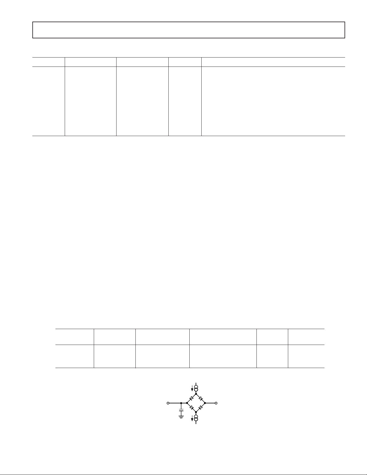
I
OL
200A
TO
OUTPUT
PIN
50pF
C
L
I
OH
200A
1.6V
Figure 1. Load Circuit for Digital Output Timing Specifications
–3–

AD7810
PIN FUNCTION DESCRIPTIONS
Pin No. Mnemonic Description
1 CONVST Convert Start. Falling edge puts the track-and-hold into hold mode and initiates a conversion.
A rising edge on the CONVST pin enables the serial port of the AD7810. This is useful in multipackage applications where a number of devices share the same serial bus. The state of this pin at
the end of conversion also determines whether the part is powered down or not. See Operating
Modes section of this data sheet.
2V
3V
IN+
IN–
4 GND Ground reference for analog and digital circuitry.
5V
6D
REF
OUT
7 SCLK Serial Clock. An external serial clock is applied here.
8VDDPositive Supply Voltage 2.7 V to 5.5 V.
Positive input of the pseudo differential analog input.
Negative input of the pseudo differential analog input.
External reference is connected here.
Serial data is shifted out on this pin.
PIN CONFIGURATION
DIP/SOIC
CONVST
V
IN
V
IN
GND
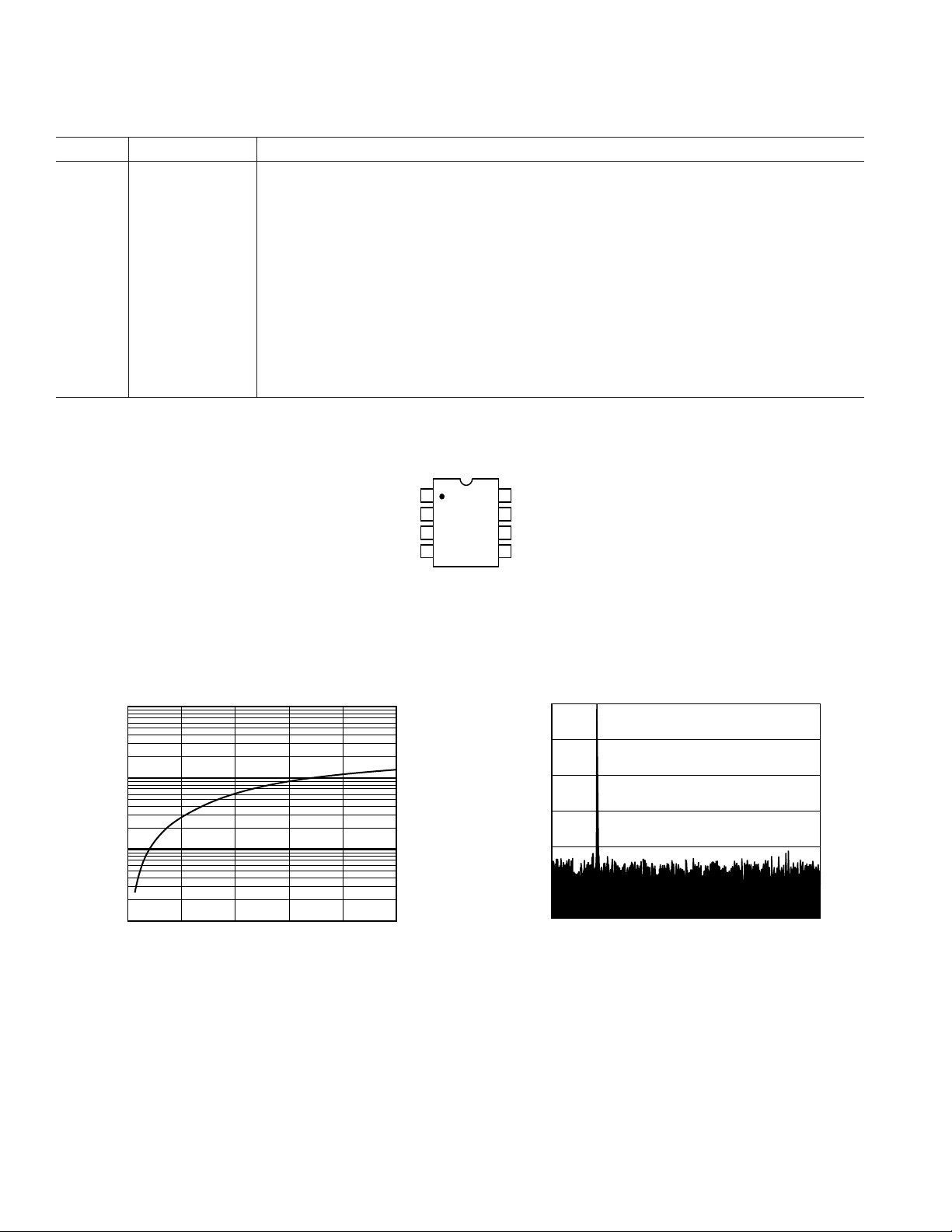
Typical Performance Characteristics
10
1
POWER – mW
0.1
0.01
030
10
THROUGHPUT – kSPS
20
40 50
1
2
+
3
–
4
AD7810
TOP VIEW
(Not to Scale)
8
7
6
5
V
DD
SCLK
D
OUT
V
REF
dBs
–115
–15
–35
–55
–75
–95
1
234567
2048 POINT FFT
SAMPLING 357.142kSPS
FIN = 30kHz
89
111
133
155
177
199
221
243
265
287
309
331
353
375
397
419
441
463
485
507
529
551
573
595
617
639
661
683
705
727
749
771
793
815
837
859
881
903
925
947
969
991
FREQUENCY BINS
1013
Figure 2. Power vs. Throughput
–4–
Figure 3. AD7810 SNR
REV. B
 Loading...