Analog Devices AD780CR-REEL7, AD780CR, AD780BR-REEL7, AD780BR-REEL, AD780BR Datasheet
...
REV. B
Information furnished by Analog Devices is believed to be accurate and
reliable. However, no responsibility is assumed by Analog Devices for its
use, nor for any infringements of patents or other rights of third parties
which may result from its use. No license is granted by implication or
otherwise under any patent or patent rights of Analog Devices.
a
2.5 V/3.0 V
High Precision Reference
AD780
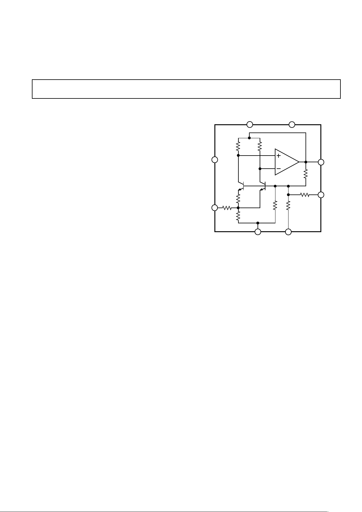
FUNCTIONAL BLOCK DIAGRAM
NC
TEMP
+V
IN
V
OUT
TRIM
GND
O/P SELECT
2.5V - NC
3.0V - GND
Q6
Q7
R10
R11
R5
R4
R14 R15
R16
R13
NC = NO CONNECT
NC
7
2
1
3
4
8
6
5
AD780
PRODUCT DESCRIPTION
The AD780 is an ultrahigh precision bandgap reference voltage
which provides a 2.5 V or 3.0 V output from inputs between
4.0 V and 36 V. Low initial error and temperature drift combined with low output noise and the ability to drive any value of
capacitance make the AD780 the ideal choice for enhancing the
performance of high resolution ADCs and DACs and for any
general purpose precision reference application. A unique low
headroom design facilitates a 3.0 V output from a 5.0 V ± 10%
input, providing a 20% boost to the dynamic range of an ADC,
over performance with existing 2.5 V references.
The AD780 can be used to source or sink up to 10 mA and can
be used in series or shunt mode, thus allowing positive or negative output voltages without external components. This makes it
suitable for virtually any high performance reference application.
Unlike some competing references, the AD780 has no “region
of possible instability.” The part is stable under all load conditions when a 1 µF bypass capacitor is used on the supply.
A temperature output pin is provided on the AD780. This provides an output voltage that varies linearly with temperature, allowing the AD780 to be configured as a temperature transducer
while providing a stable 2.5 V or 3.0 V output.
The AD780 is a pin-compatible performance upgrade for the
LT1019(A)–2.5 and the AD680. The latter is targeted toward
low power applications.
The AD780 is available in three grades in plastic DIP, SOIC,
and cerdip packages. The AD780AN, AD780AR, AD780BN,
AD780BR, and AD780CR are specified for operation from –40°C
to +85°C.
FEATURES
Pin-Programmable 2.5 V or 3.0 V Output
Ultralow Drift: 3 ppm/C max
High Accuracy: 2.5 V or 3.0 V 1 mV max
Low Noise: 100 nV/
√
Hz
Noise Reduction Capability
Low Quiescent Current: 1 mA max
Output Trim Capability
Plug-In Upgrade for Present References
Temperature Output Pin
Series or Shunt Mode Operation (2.5 V, 3.0 V)
PRODUCT HIGHLIGHTS
1. The AD780 provides a pin-programmable 2.5 V or 3.0 V
output from a 4 V to 36 V input.
2. Laser trimming of both initial accuracy and temperature
coefficients results in low errors over temperature without the
use of external components. The AD780BN has a maximum
variation of 0.9 mV from –40°C to +85°C.
3. For applications requiring even higher accuracy, an optional
fine-trim connection is provided.
4. The AD780 noise is extremely low, typically 4 µV p-p from
0.1 Hz to 10 Hz and a wideband spectral noise density of
typically 100 nV/√Hz. This can be further reduced if desired,
by simply using two external capacitors.
5. The temperature output pin enables the AD780 to be configured as a temperature transducer while providing a stable
output reference voltage.
One Technology Way, P.O. Box 9106, Norwood, MA 02062-9106, U.S.A.
Tel: 781/329-4700 World Wide Web Site: http://www.analog.com
Fax: 781/326-8703 © Analog Devices, Inc., 2000

AD780–SPECIFICATIONS
AD780AN/AR AD780CR AD780BN/BR
Parameter Min Typ Max Min Typ Max Min Typ Max Unit
OUTPUT VOLTAGE
2.5 V Out 2.495 2.505 2.4985 2.5015 2.499 2.501 Volts
3.0 V Out 2.995 3.005 2.9950 3.0050 2.999 3.001 Volts
OUTPUT VOLTAGE DRIFT
1
–40°C to +85°C 7 7 3 ppm/°C
–55°C to +125°C 20 20 ppm/°C
LINE REGULATION
2.5 V Output, 4 V ≤ +V
IN
≤ 36 V
T
MIN
to T
MAX
10 * * µV/V
3.0 V Output, 4.5 V ≤ +V
IN
≤ 36 V
T
MIN
to T
MAX
10 * * µV/V
LOAD REGULATION, SERIES MODE
Sourcing 0 < I
OUT
< 10 mA 50 * * µV/mA
T
MIN
to T
MAX
75 * * µV/mA
Sinking –10 < I
OUT
< 0 mA 75 * * µV/mA
–40°C to +85°C75**µV/mA
–55°C to +125°C 150 * * µV/mA
LOAD REGULATION, SHUNT MODE
I < I
SHUNT
< 10 mA 75 * * µV/mA
QUIESCENT CURRENT, 2.5 V SERIES MODE
2
–40°C to +85°C 0.75 1.0 * * * * mA
–55°C to +125°C 0.8 1.3 * * * * mA
MINIMUM SHUNT CURRENT 0.7 1.0 * * * * mA
OUTPUT NOISE
0.1 Hz to 10 Hz 4 * * * * µV p-p
Spectral Density, 100 Hz 100 * * * * nV/√Hz
LONG TERM STABILITY
3
20 * * ±ppm/
1000 Hr
TRIM RANGE 4.0 * * ±%
TEMPERATURE PIN
Voltage Output @ 25°C 500 560 620 * * * * * * mV
Temperature Sensitivity 1.9 * * mV/°C
Output Resistance 3 * * kΩ
SHORT CIRCUIT CURRENT TO GROUND 30 * * mA
TEMPERATURE RANGE
Specified Performance (A, B, C) –40 +85 * * * * °C
Operating Performance (A, B, C)
4
–55 +125 * * * * °C
Specified Performance (S) –55 +125 * * * * °C
Operating Performance (S) –55 +125 * * * * ° C
NOTES
1
Maximum output voltage drift is guaranteed for all packages.
2
3.0 V mode typically adds 100 µA to the quiescent current. Also, Iq increases by 2 µA/V above an input voltage of 5 V.
3
The long term stability specification is noncumulative. The drift in subsequent 1000 hr. periods is significantly lower than in the first 1000 hr. period.
4
The operating temperature range is defined as the temperature extremes at which the device will still function. Parts may deviate from their specified performance
outside their specified temperature range.
*Same as AD780AN/AR specification.
Specifications subject to change without notice.
REV. B
–2–
(TA = +25C, VIN = +5 V unless otherwise noted)

AD780
REV. B
–3–
ORDERING GUIDE
Initial Temperature Temperature Package
Model Error Range Coefficient Options
AD780AN ⫾5.0 mV –40°C to +85°C 7 ppm/°C Plastic Dip
AD780AR ⫾5.0 mV –40°C to +85°C 7 ppm/°C SOIC
AD780AR-REEL7 ⫾5.0 mV –40°C to +85°C 7 ppm/°C SOIC
AD780BN ⫾1.0 mV –40°C to +85°C 3 ppm/°C Plastic Dip
AD780BR ⫾1.0 mV –40°C to +85°C 3 ppm/°C SOIC
AD780BR-REEL ⫾1.0 mV –40°C to +85°C 3 ppm/°C SOIC
AD780BR-REEL7 ⫾1.0 mV –40°C to +85°C 3 ppm/°C SOIC
AD780CR ⫾ 1.5 mV –40°C to +85°C 7 ppm/°C SOIC
AD780CR-REEL7 ⫾1.5 mV –40°C to +85°C 7 ppm/°C SOIC
ABSOLUTE MAXIMUM RATINGS*
VIN to Ground . . . . . . . . . . . . . . . . . . . . . . . . . . . . . . . . . .36 V
Trim Pin to Ground . . . . . . . . . . . . . . . . . . . . . . . . . . . . . 36 V
Temp Pin to Ground . . . . . . . . . . . . . . . . . . . . . . . . . . . . . 36 V
Power Dissipation (25°C) . . . . . . . . . . . . . . . . . . . . . . 500 mW
Storage Temperature . . . . . . . . . . . . . . . . . . .–65°C to +150°C
Lead Temperature (Soldering, 10 sec) . . . . . . . . . . . . . 300°C
Output Protection: Output safe for indefinite short to ground
and momentary short to V
IN
.
ESD Classification . . . . . . . . . . . . . . . . . . . . . Class 1 (1000 V)
*Stresses above those listed under Absolute Maximum Ratings may cause perma-
nent damage to the device. This is a stress rating only; functional operation of the
device at these or any conditions above those indicated in the operational specification is not implied. Exposure to absolute maximum specifications for extended
periods may affect device reliability.
PIN CONFIGURATION
8-Lead Plastic DIP, SOIC and Cerdip Packages
1
2
3
4
8
7
6
5
TOP VIEW
(Not to Scale)
AD780
2.5/3.0V SELECT
(NC OR GND)
NC
V
OUT
TRIM
NC
+V
IN
TEMP
GND
NC = NO CONNECT
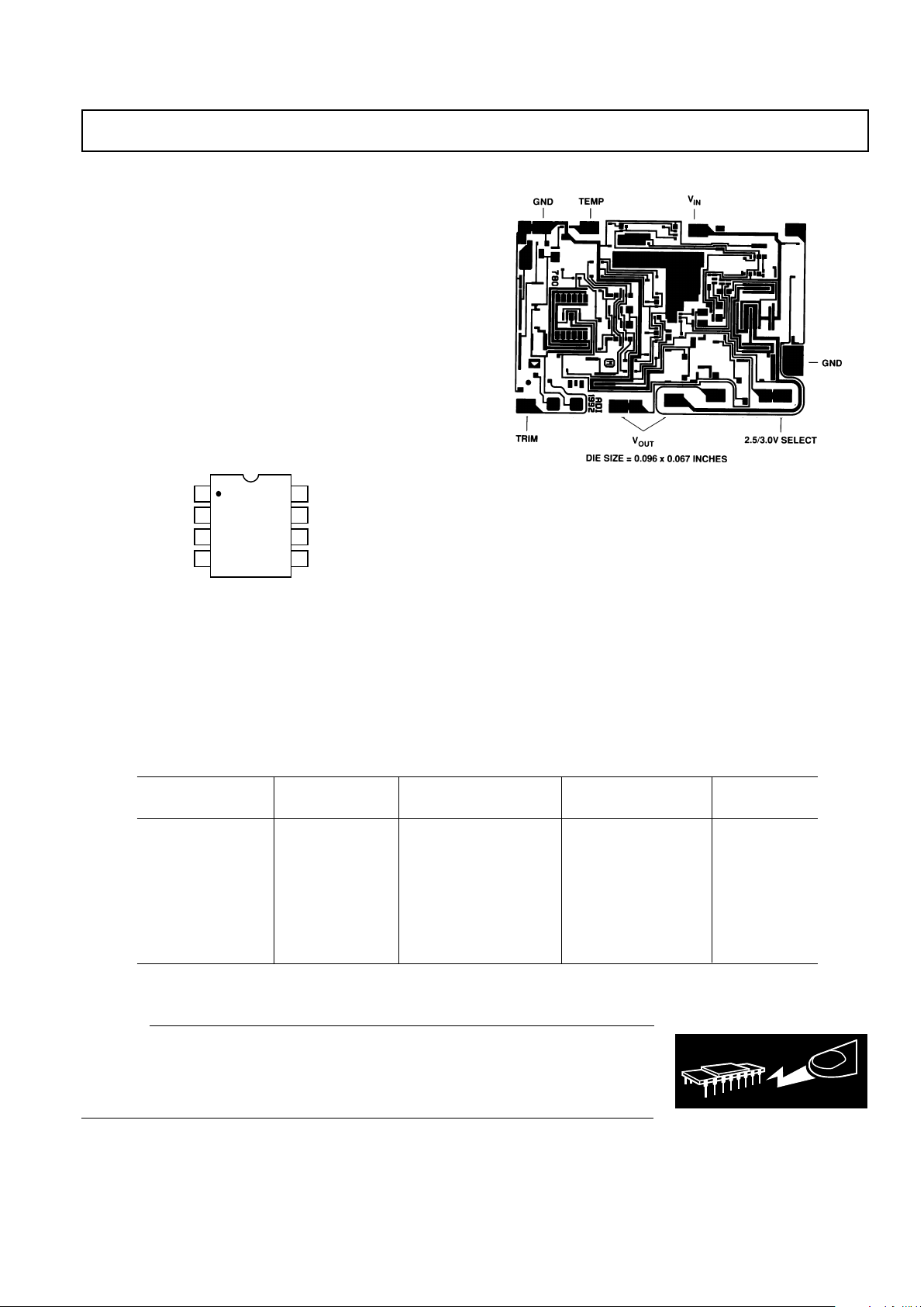
DIE LAYOUT
NOTES
Both V
OUT
pads should be connected to the output
Die Thickness: The standard thickness of Analog Devices Bipolar dice is
24 mils ±2 mils.
Die Dimensions: The dimensions given have a tolerance of ± 2 mils.
Backing: The standard backside surface is silicon (not plated). Analog Devices
does not recommend gold-backed dice for most applications.
Edges: A diamond saw is used to separate wafers into dice thus providing perpendicular edges half-way through the die.
In contrast to scribed dice, this technique provides a more uniform die shape
and size. The perpendicular edges facilitate handling (such as tweezer pick-up)
while the uniform shape and size simplifies substrate design and die attach.
Top Surface: The standard top surface of the die is covered by a layer of
glassivation. All areas are covered except bonding pads and scribe lines.
Surface Metalization: The metalization to Analog Devices bipolar dice is aluminum. Minimum thickness is 10,000Å.
Bonding Pads: All bonding pads have a minimum size of 4.0 mils by 6.0 mils.
The passivation windows have a 3.6 mils by 5.6 mils minimum size.
CAUTION
ESD (electrostatic discharge) sensitive device. Electrostatic charges as high as 4000 V readily
accumulate on the human body and test equipment and can discharge without detection.
Although the AD780 features proprietary ESD protection circuitry, permanent damage may
occur on devices subjected to high-energy electrostatic discharges. Therefore, proper ESD
precautions are recommended to avoid performance degradation or loss of functionality.
WARNING!
ESD SENSITIVE DEVICE
 Loading...