

Analog Devices AD7794 Datasheet
6-Channel, Low Noise, Low Power, 24-Bit
∑-Δ
FEATURES
Up to 22.5 effective bits
RMS noise: 40 nV @ 4.17 Hz
85 nV @ 16.7 Hz
Current: 400 µA typ
Power-down: 1 µA max
Low noise programmable gain instrumentation-amp
Band gap reference with 4 ppm/°C drift typ
Update rate: 4.17 Hz to 500 Hz
Six differential analog inputs
Internal clock oscillator
Simultaneous 50 Hz/60 Hz rejection
Reference detect
Programmable current sources
On-chip bias voltage generator
Burnout currents
Low-side power switch
Power supply: 2.7 V to 5.25 V
–40°C to +105°C temperature range
Independent interface power supply
24-lead TSSOP package
INTERFACE
3-wire serial
SPI®-, QSPI™-, MICROWIRE™-, and DSP-compatible
Schmitt trigger on SCLK
APPLICATIONS
Temperature measurement
Pressure measurement
Weigh scales
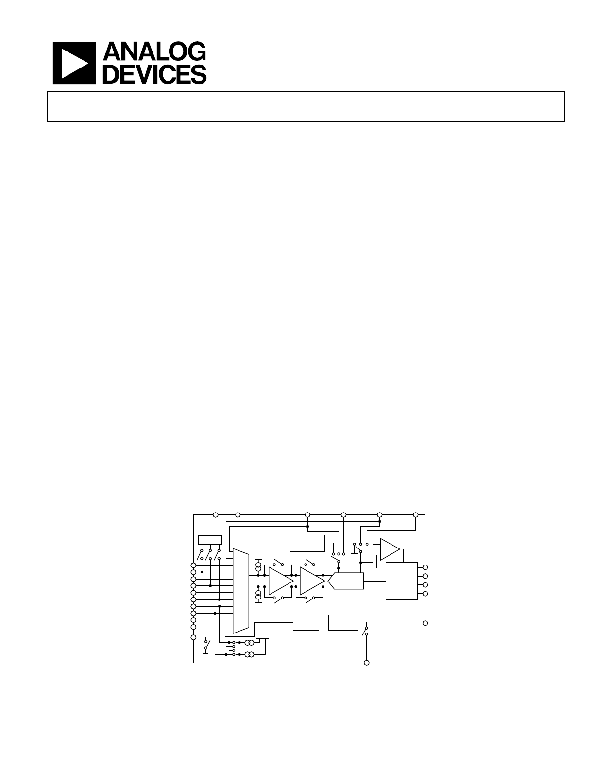
FUNCTIONAL BLOCK DIAGRAM
GND AV
DD
ADC with On-Chip In-Amp and Reference
AD7794
Strain gauge transducers
Gas analysis
Industrial process control
Instrumentation
Blood analysis
Smart transmitters
Liquid/gas chromotography
6-digit DVM
GENERAL DESCRIPTION
The AD7794 is a low power, low noise, complete analog front
end for high precision measurement applications. It contains a
low noise, 24-bit ∑-∆ ADC with six differential inputs. The
on-chip low noise instrumentation amplifier means that signals
of small amplitude can be interfaced directly to the ADC.
The device contains a precision low noise, low drift internal
band gap reference and can also accept up to two external
differential references. Other on-chip features include programmable excitation current sources, burnout currents and a bias
voltage generator, this feature being used to set the common
mode voltage of a channel to AV
switch can be used to power down bridge sensors between
conversions, minimizing the system’s power consumption. The
device can be operated with the internal clock or, alternatively,
an external clock can be used. The output data rate from the
part can be varied from 4.17 Hz to 500 Hz.
The part operates with a power supply from 2.7 V to 5.25 V. It
consumes a current of 400 µA typical and is housed in a 24-lead
TSSOP package.
AIN4(+)/REFIN2(+) REFIN1(+) AIN4(–)/REFIN2(–) REFIN1(–)
/2. The low-side power
DD
V
BIAS
V
MUX
GND
DD
V
DD
AIN1(+)
AIN1(–)
AIN2(+)
AIN2(–)
AIN3(+)
AIN3(–)
AIN5(+)/IOUT2
AIN5(–)/IOUT1
AIN6(+)/P1
AIN6(+)/P2
PSW
GND
Rev. 0
Information furnished by Analog Devices is believed to be accurate and reliable.
However, no responsibility is assumed by Analog Devices for its use, nor for any
infringements of patents or other rights of third parties that may result from its use.
Specifications subject to change without notice. No license is granted by implication
or otherwise under any patent or patent rights of Analog Devices. Trademarks and
registered trademarks are the property of their respective owners.
BAND GAP
REFERENCE
IN-AMPBUF
TEMP
SENSOR
Figure 1.
REFERENCE
DETECT
GND
SERIAL
CLK
INTERFACE
AND
LOGIC
CONTROL
AD7794
Σ-∆
ADC
INTERNAL
CLOCK
One Technology Way, P.O. Box 9106, Norwood, MA 02062-9106, U.S.A.
Tel: 781.329.4700 www.analog.com
Fax: 781.326.8703 © 2004 Analog Devices, Inc. All rights reserved.
DOUT/RDY
DIN
SCLK
CS
DV
DD
04854-001

AD7794
TABLE OF CONTENTS
Specifications..................................................................................... 3
Timing Characteristics..................................................................... 7
Absolute Maximum Ratings............................................................ 9
ESD Caution.................................................................................. 9
Pin Configuration and Function Descriptions........................... 10
Output Noise and Resolution Specifications .............................. 12
Chopping Enabled...................................................................... 12
External Reference ................................................................. 12
Internal Reference.................................................................. 13
Chopping Disabled..................................................................... 14
Typical Performance Characteristics ...........................................15
On-Chip Registers.......................................................................... 16
Communications Register......................................................... 16
Status Register............................................................................. 17
Mode Register ............................................................................. 17
Single Conversion Mode....................................................... 26
Continuous Conversion Mode ............................................. 26
Continuous Read........................................................................ 27
Circuit Description......................................................................... 28
Analog Input Channel ............................................................... 28
Instrumentation Amplifier........................................................ 28
Bipolar/Unipolar Configuration .............................................. 28
Data Output Coding .................................................................. 28
Burnout Currents....................................................................... 29
Excitation Currents .................................................................... 29
Bias Voltage Generator .............................................................. 29
Reference ..................................................................................... 29
Reference Detect......................................................................... 30
Reset ............................................................................................. 30
AV
Monitor ............................................................................. 30
DD
Configuration Register ..............................................................19
Data Register............................................................................... 21
ID Register................................................................................... 21
IO Register................................................................................... 21
Offset Register............................................................................. 22
Full-Scale Register ...................................................................... 22
ADC Circuit Information.............................................................. 23
Overview...................................................................................... 23
Digital Interface.......................................................................... 25
REVISION HISTORY
10/04—Revision 0: Initial Version
Calibration................................................................................... 30
Grounding and Layout .............................................................. 31
Applications..................................................................................... 32
Flowmeter.................................................................................... 32
Outline Dimensions....................................................................... 33
Ordering Guide .......................................................................... 33
Rev. 0 | Page 2 of 36
AD7794
SPECIFICATIONS
AVDD = 2.7 V to 5.25 V; DVDD = 2.7 V to 5.25 V; GND = 0 V; all specifications T
Table 1.
Parameter1 AD7794B Unit Test Conditions/Comments
AD7794 (CHOP ENABLED)
Output Update Rate 4.17 – 500 Hz nom Settling Time = 2/Output Update Rate
No Missing Codes2 24 Bits min f
Resolution See Tables in ADC
Description
Output Noise and Update Rates See Tables in ADC
Description
Integral Nonlinearity ±15 ppm of FSR max
Offset Error3 ±1 µV typ
Offset Error Drift vs. Temperature4 ±10 nV/°C typ
Full-Scale Error
3, 5
Gain Drift vs. Temperature4
±10 µV typ
±1 ppm/°C typ Gain = 1 to 16, External Reference
±3 ppm/°C typ Gain = 32 to 128, External Reference
Power Supply Rejection 100 dB min AIN = 1 V/Gain, Gain ≥ 4, External Reference
ANALOG INPUTS
Differential Input Voltage Ranges ± V
Absolute AIN Voltage Limits2
/Gain V nom V
REF
Unbuffered Mode GND – 30 mV V min Gain = 1 or 2
AVDD + 30 mV V max
Buffered Mode GND + 100 mV V min Gain = 1 or 2
AVDD – 100 mV V max
In-Amp Active GND + 300 mV V min Gain = 4 to 128
AVDD – 1.1 V max
Common-Mode Voltage, VCM 0.5 V min VCM = (AIN(+) + AIN(–))/2, Gain = 4 to 128
Analog Input Current
Buffered Mode or In-Amp Active
Average Input Current2
±1 nA max Gain = 1 or 2, Update Rate < 100 Hz
±250 pA max Gain = 4 to 128, Update Rate < 100 Hz
±1 nA max AIN6(+)/AIN6(−)
Average Input Current Drift ±2 pA/°C typ
Unbuffered Mode Gain = 1 or 2
Average Input Current ±400 nA/V typ Input current varies with input voltage
Average Input Current Drift ±50 pA/V/°C typ
Normal Mode Rejection2
Internal Clock
@ 50 Hz, 60 Hz 65 dB min 80 dB typ, 50 ± 1 Hz, 60 ± 1 Hz, FS[3:0] = 10106
@ 50 Hz 80 dB min
@ 60 Hz 90 dB min
External Clock
@ 50 Hz, 60 Hz 80 dB min
@ 50 Hz 94 dB min
@ 60 Hz 90 dB min
Common-Mode Rejection
@ DC 100 dB min AIN = 1 V/Gain, Gain ≥ 4
@ 50 Hz, 60 Hz2
@ 50 Hz, 60 Hz2
100 dB min
100 dB min
MIN
to T
, unless otherwise noted.
MAX
≤ 250 Hz
ADC
= REFIN(+) – REFIN(−) or Internal Reference,
REF
Gain = 1 to 128
6
90 dB typ, 50 ± 1 Hz, FS[3:0] = 1001
100 dB typ, 60 ± 1 Hz, FS[3:0] = 1000
6
90 dB typ, 50 ± 1 Hz, 60 ± 1 Hz, FS[3:0] = 1010
6
100 dB typ, 50 ± 1 Hz, FS[3:0] = 1001
100 dB typ, 60 ± 1 Hz, FS[3:0] = 1000
6
50 ± 1 Hz, 60 ± 1 Hz, FS[3:0] = 10106
50 ± 1 Hz (FS[3:0] = 10016), 60 ± 1 Hz (FS[3:0] = 10006)
6
Rev. 0 | Page 3 of 36

AD7794
Parameter1 AD7794B Unit Test Conditions/Comments
AD7794 (CHOP DISABLED)
Output Update Rate 4.17 - 500 Hz nom Settling Time = 1/Output Update Rate
No Missing Codes2
Resolution See Tables in ADC
Output Noise and Update Rates See Tables in ADC
Integral Nonlinearity ±15 ppm of FSR max
Offset Error3
Offset Error Drift vs. Temperature4
10 nV/°C typ Gain = 32 to 128
Full-Scale Error
3, 5
Gain Drift vs. Temperature4
±3 ppm/°C typ Gain = 32 to 128, External Reference
Power Supply Rejection 100 dB typ AIN = 1 V/Gain, Gain ≥ 4, External Reference
ANALOG INPUTS
Differential Input Voltage Ranges ± V
Absolute AIN Voltage Limits2
Unbuffered Mode GND – 30 mV V min Gain = 1 or 2
AVDD + 30 mV V max
Buffered Mode GND + 100 mV V min Gain = 1 or 2
AVDD – 100 mV V max
In-Amp Active GND + 300 mV V min Gain = 4 to 128
AVDD – 1.1 V max
Common-Mode Voltage, VCM 0.2 + (Gain/2 x
AVDD – 0.2 – (Gain/2
Analog Input Current
Buffered Mode or In-Amp Active
Average Input Current2
±250 pA max Gain = 4 to 128
±1 nA max AIN6(+)/AIN6(−)
Average Input Current Drift ±2 pA/°C typ
Unbuffered Mode Gain = 1 or 2
Average Input Current ±400 nA/V typ Input current varies with input voltage.
Average Input Current Drift ±50 pA/V/°C typ
Normal Mode Rejection2
Internal Clock
@ 50 Hz, 60 Hz 60 dB min
@ 50 Hz 78 dB min
@ 60 Hz 86 dB min
External Clock
@ 50 Hz, 60 Hz 60 dB min
@ 50 Hz 94 dB min
@ 60 Hz 90 dB min
Common-Mode Rejection
@ DC 100 dB min AIN = 1 V/Gain with Gain = 4, AMP-CM Bit = 1
@ 50 Hz, 60 Hz2
@ 50 Hz, 60 Hz2
24 Bits min f
≤125 Hz
ADC
Description
Description
±100/Gain µV typ Without Calibration
±100/Gain nV/°C typ Gain = 1 to 16
±10 µV typ
±1 ppm/°C typ Gain = 1 to 16, External Reference
/Gain V nom V
REF
= REFIN(+)− REFIN(−) or Internal Reference,
REF
Gain = 1 to 128
V min AMP-CM = 1, VCM = (AIN(+) + AIN(–))/2, Gain = 4 to 128
(AIN(+) – AIN(-)))
V max
x (AIN(+) – AIN(-)))
±1 nA max Gain = 1 or 2
70 dB typ, 50 ± 1 Hz, 60 ± 1 Hz, FS[3:0] = 1010
90 dB typ, 50 ± 1 Hz, FS[3:0] = 1001
100 dB typ, 60 ± 1 Hz, FS[3:0] = 1000
70 dB typ, 50 ± 1 Hz, 60 ± 1 Hz, FS[3:0] = 1010
100 dB typ, 50 ± 1 Hz, FS[3:0] = 1001
100 dB typ, 60 ± 1 Hz, FS[3:0] = 1000
100 dB min
100 dB min
50 ± 1 Hz, 60 ± 1 Hz, FS[3:0] = 10106
50 ± 1 Hz (FS[3:0] = 10016), 60 ± 1 Hz (FS[3:0] = 10006)
6
6
6
6
6
6
Rev. 0 | Page 4 of 36
AD7794
Parameter1 AD7794B Unit Test Conditions/Comments
AD7794 (CHOP ENABLED or DISABLED)
REFERENCE INPUT
Internal Reference
Internal Reference Initial Accuracy 1.17 ±0.01% V min/max
Internal Reference Drift2
15 ppm/°C max
Power Supply Rejection 85 dB typ
External Reference
External REFIN Voltage 2.5 V nom REFIN = REFIN(+) – REFIN(–)
Reference Voltage Range2
AVDD V max When V
Absolute REFIN Voltage Limits2
AVDD + 30 mV V max
Average Reference Input Current 400 nA/V typ
Average Reference Input Current
Drift
Normal Mode Rejection2
Common-Mode Rejection 100
Reference Detect Levels 0.3 V min
0.65 V max NOXREF Bit Active if V
EXCITATION CURRENT SOURCES
(IEXC1 and IEXC2)
Output Current 10/210/1000 µA nom
Initial Tolerance at 25°C ±5 % typ
Drift 200 ppm/°C typ
Current Matching ±0.5 % typ Matching between IEXC1 and EXC2. V
Drift Matching 50 ppm/°C typ
Line Regulation (AVDD) 2 %/V typ AVDD = 5 V ± 5%
Load Regulation 0.2 %/V typ
Output Compliance AVDD – 0.65 V max Current Sources Programmed to 10 µA or 210 µA
AVDD – 1.1 V max Current Sources Programmed to 1 mA
GND – 30 mV V min
BIAS VOLTAGE GENERATOR
V
AVDD/2 V nom
BIAS
V
Generator Start-Up Time
BIAS
TEMPERATURE SENSOR
Accuracy
Sensitivity
LOW SIDE POWER SWITCH
RON 7 Ω max AVDD = 5 V
9 Ω max AVDD = 3 V
Allowable Current2
DIGITAL OUTPUTS (P1 and P2)
VOH, Output High Voltage2
VOL, Output Low Voltage2
VOH, Output High Voltage2
VOL, Output Low Voltage2
INTERNAL/EXTERNAL CLOCK
Internal Clock
Frequency2
Duty Cycle 50:50 % typ
AVDD = 4 V, TA = 25°C
4 ppm/°C typ
0.1 V min
= AVDD , the differential input must be limited to
REF
/Gain if the In-Amp is active
0.9×V
REF
GND – 30 mV V min
±0.03 nA/V/°C typ
Same as for Analog
Inputs
See
± 2
0.81
Figure 11
dB typ
ms/nF typ Dependent on the Capacitance connected to AIN
°C typ Applies if User Calibrates the Temp Sensor
mV/°C typ
30 mA max Continuous Current
AV
− 0.6 V min AVDD = 3 V, I
DD
0.4 V max AV
4 V min AV
0.4 V max AV
= 3 V, I
DD
= 5 V, I
DD
= 5 V, I
DD
= 100 µA
SOURCE
= 100 µA
SINK
= 200 µA
SOURCE
= 800 µA
SINK
64 ± 3% kHz min/max
< 0.3 V
REF
OUT
= 0 V
Rev. 0 | Page 5 of 36

AD7794
Parameter1 AD7794B Unit Test Conditions/Comments
External Clock
Frequency 64 kHz nom A 128 kHz external clock can be used if the divide by 2
Duty Cycle 45:55 to 55:45 % typ
LOGIC INPUTS
2
CS
V
, Input Low Voltage 0.8 V max DVDD = 5 V
INL
0.4 V max DVDD = 3 V
V
, Input High Voltage 2.0 V min DVDD = 3 V or 5 V
INH
SCLK, CLK and DIN (Schmitt-Triggered
Input)
2
VT(+) 1.4/2 V min/V max DVDD = 5 V
VT(–) 0.8/1.7 V min/V max DVDD = 5 V
VT(+) − VT(−)
0.1/0.17 V min/V max DV
VT(+) 0.9/2 V min/V max DVDD = 3 V
VT(−) 0.4/1.35 V min/V max DVDD = 3 V
VT(+)− VT(−) 0.06/0.13 V min/V max DVDD = 3 V
Input Currents ±10 µA max VIN = DVDD or GND
Input Capacitance 10 pF typ All Digital Inputs
LOGIC OUTPUTS (Including CLK)
DV
VOH, Output High Voltage2
VOL, Output Low Voltage2
VOH, Output High Voltage2
VOL, Output Low Voltage2
– 0.6 V min DVDD = 3 V, I
DD
0.4 V max DV
4 V min DV
0.4 V max
Floating-State Leakage Current ±10 µA max
Floating-State Output Capacitance 10 pF typ
Data Output Coding Offset Binary
SYSTEM CALIBRATION2
Full-Scale Calibration Limit 1.05 × FS V max
Zero-Scale Calibration Limit −1.05 × FS V min
Input Span 0.8 × FS V min
2.1 × FS V max
POWER REQUIREMENTS7
Power Supply Voltage
AVDD – GND 2.7/5.25 V min/max
DVDD – GND 2.7/5.25 V min/max
Power Supply Currents
IDD Current 140 µA max
185 µA max
400 µA max
500 µA max
IDD (Power-Down Mode) 1 µA max
1
Temperature Range: −40°C to +105°C.
2
Specification is not production tested but is supported by characterization data at initial product release.
3
Following a calibration, this error will be in the order of the noise for the programmed gain and update rate selected.
4
Recalibration at any temperature will remove these errors.
5
Full-scale error applies to both positive and negative full-scale and applies at the factory calibration conditions (AVDD = 4 V, gain = 1, TA = 25°C ).
6
FS[3:0] are the four bits used in the mode register to select the output word rate.
7
Digital inputs equal to DV
or GND with excitation currents and bias voltage generator disabled.
DD
function is used (Bit CLK1 = CLK0 = 1)
Applies for external 64 kHz clock.
have a less stringent duty cycle
= 5 V
DD
= 100 µA
SOURCE
= 3 V, I
DD
= 5 V, I
DD
DV
= 5 V, I
DD
110 µA typ @ AV
= 100 µA
SINK
= 200 µA
SOURCE
= 1.6 mA (DOUT/
SINK
= 3 V, 125 µA typ @ AVDD = 5 V,
DD
A 128 kHz clock can
RDY
)/800 µA (CLK)
Unbuffered Mode, Ext. Reference
130 µA typ @ AV
= 3 V, 165 µA typ @ AVDD = 5 V,
DD
Buffered Mode, Gain = 1 or 2, Ext Ref
300 µA typ @ AV
= 3 V, 350 µA typ @ AVDD = 5 V,
DD
Gain = 4 to 128, Ext. Ref
400 µA typ @ AV
= 3 V, 450 µA typ @ AVDD = 5 V,
DD
Gain = 4 to 128, Int Ref
Rev. 0 | Page 6 of 36
AD7794
TIMING CHARACTERISTICS
AVDD = 2.7 V to 5.25 V; DVDD = 2.7 V to 5.25 V; GND = 0 V, Input Logic 0 = 0 V, Input Logic 1 = DVDD, unless otherwise noted.
Table 2.
Parameter
t
3
t4 100 ns min SCLK Low Pulse Width
Read Operation
t1 0 ns min
60 ns max DVDD = 4.75 V to 5.25 V
80 ns max DVDD = 2.7 V to 3.6 V
t
2
60 ns max DVDD = 4.75 V to 5.25 V
80 ns max DVDD = 2.7 V to 3.6 V
t
5
80 ns max
t6 0 ns min
t7 10 ns min
Write Operation
t8 0 ns min
t9 30 ns min Data Valid to SCLK Edge Setup Time
t10 25 ns min Data Valid to SCLK Edge Hold Time
t11 0 ns min
1, 2
Limit at T
MIN
, T
(B Version) Unit Conditions/Comments
MAX
100 ns min SCLK High Pulse Width
Falling Edge to DOUT/RDY Active Time
CS
3
0 ns min SCLK Active Edge to Data Valid Delay4
5, 6
10 ns min
Bus Relinquish Time after CS
SCLK Inactive Edge to CS
SCLK Inactive Edge to DOUT/RDY
Falling Edge to SCLK Active Edge Setup Time4
CS
Rising Edge to SCLK Edge Hold Time
CS
Inactive Edge
Inactive Edge
High
1
Sample tested during initial release to ensure compliance. All input signals are specified with tR = tF = 5 ns (10% to 90% of DVDD) and timed from a voltage level of 1.6 V.
2
See Figure 3 and Figure 4.
3
These numbers are measured with the load circuit of Figure 2 and defined as the time required for the output to cross the VOL or VOH limits.
4
SCLK active edge is falling edge of SCLK.
5
These numbers are derived from the measured time taken by the data output to change 0.5 V when loaded with the circuit of Figure 2. The measured number is then
extrapolated back to remove the effects of charging or discharging the 50 pF capacitor. This means that the times quoted in the timing characteristics are the true bus
relinquish times of the part and, as such, are independent of external bus loading capacitances.
6
RDY
returns high after a read of the ADC. In single conversion mode and continuous conversion mode, the same data can be read again, if required, while
although care should be taken to ensure that subsequent reads do not occur close to the next output update. In continuous read mode, the digital word can be read
only once.
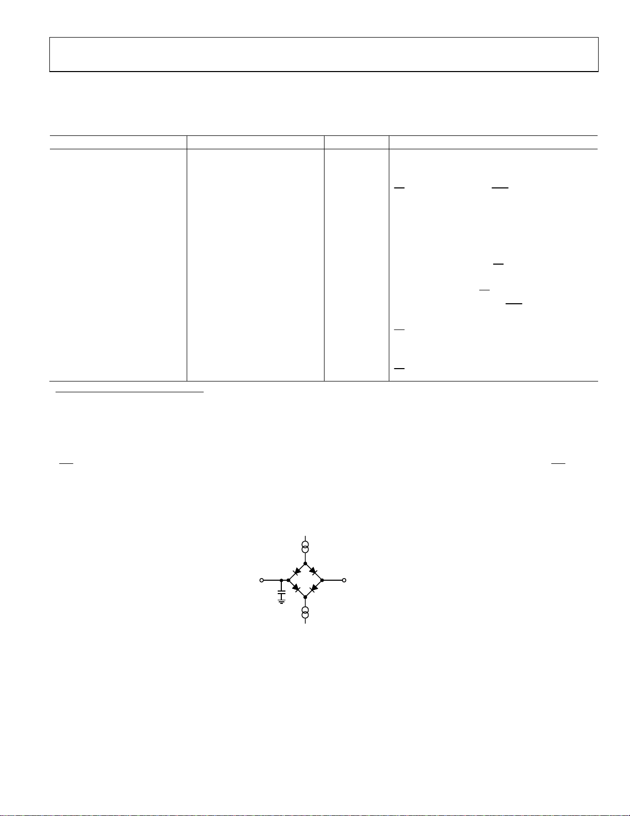
RDY
is high,
I
(1.6mA WITH DVDD = 5V,
SINK
OUTPUT
PIN
TO
50pF
100µA WITH DV
I
SOURCE
100µA WITH DV
= 3V)
DD
1.6V
(200µA WITH DVDD = 5V,
= 3V)
DD
04854-002
Figure 2. Load Circuit for Timing Characterization
Rev. 0 | Page 7 of 36
AD7794
S
CS (I)
DOUT/RDY (O)
SCLK (I)
CS (I)
t
1
MSB LSB
t
2
t
3
t
I = INPUT, O = OUTPUT
4
Figure 3. Read Cycle Timing Diagram
t
6
t
5
t
7
04854-003
t
11
04854-004
CLK (I)
DIN (I)
I = INPUT, O = OUTPUT
t
8
t
9
t
10
MSB LSB
Figure 4. Write Cycle Timing Diagram
Rev. 0 | Page 8 of 36

AD7794
ABSOLUTE MAXIMUM RATINGS
TA= 25°C, unless otherwise noted.
Table 3.
Parameter Rating
AVDD to GND –0.3 V to +7 V
DVDD to GND –0.3 V to +7 V
Analog Input Voltage to GND –0.3 V to AVDD + 0.3 V
Reference Input Voltage to GND –0.3 V to AVDD + 0.3 V
Digital Input Voltage to GND –0.3 V to DVDD + 0.3 V
Digital Output Voltage to GND –0.3 V to DVDD + 0.3 V
AIN/Digital Input Current 10 mA
Operating Temperature Range –40°C to +85°C
Storage Temperature Range –65°C to +85°C
Maximum Junction
Temperature
TSSOP
θJA Thermal Impedance 97.9°C/W
θJC Thermal Impedance 14°C/W
Lead Temperature, Soldering
Vapor Phase (60 sec) 215°C
Infrared (15 sec) 220°C
150°C
Stresses above those listed under Absolute Maximum Ratings
may cause permanent damage to the device. This is a stress
rating only; functional operation of the device at these or any
other conditions above those listed in the operational sections
of this specification is not implied. Exposure to absolute
maximum rating conditions for extended periods may affect
device reliability.
ESD CAUTION
ESD (electrostatic discharge) sensitive device. Electrostatic charges as high as 4000 V readily accumulate on the
human body and test equipment and can discharge without detection. Although this product features
proprietary ESD protection circuitry, permanent damage may occur on devices subjected to high energy
electrostatic discharges. Therefore, proper ESD precautions are recommended to avoid performance
degradation or loss of functionality.
Rev. 0 | Page 9 of 36
AD7794
A
A
PIN CONFIGURATION AND FUNCTION DESCRIPTIONS
SCLK
1
2
CLK
3
CS
NC
AIN1(+)
AIN1(–)
AIN2(+)
AIN2(–)
AIN3(+)
AIN3(–)
4
5
AD7794
6
TOP VIEW
7
(Not to Scale)
8
9
10
11
12
NC = NO CONNECT
IN6(+)/P1
IN6(–)/P2
Figure 5. Pin Configuration
Table 4. Pin Function Descriptions
Pin
No. Mnemonic Description
1 SCLK Serial Clock Input for Data Transfers to and from the ADC. The SCLK has a Schmitt-triggered input, making the interface
2 CLK Clock In/Clock Out. The internal clock can be made available at this pin. Alternatively, the internal clock can be disabled
3
CS
Chip Select Input. This is an active low logic input used to select the ADC. CS can be used to select the ADC in systems
4 NC No Connect.
5 AIN6(+)/P1 Analog Input/Digital Output Pin. AIN6(+) is the positive terminal of the differential analog input pair AIN6(+)/AIN6(−).
6 AIN6(−)/P2
7 AIN1(+) Analog Input. AIN1(+) is the positive terminal of the differential analog input pair AIN1(+)/AIN1(−).
8 AIN1(−) Analog Input. AIN1(−) is the negative terminal of the differential analog input pair AIN1(+)/AIN1(−).
9 AIN2(+) Analog Input. AIN2(+) is the positive terminal of the differential analog input pair AIN2(+)/AIN2(−).
10 AIN2(−) Analog Input. AIN2(−) is the negative terminal of the differential analog input pair AIN2(+)/AIN2(−).
11 AIN3(+) Analog Input. AIN3(+) is the positive terminal of the differential analog input pair AIN3(+)/AIN3(−).
12 AIN3(−) Analog Input. AIN3(−) is the negative terminal of the differential analog input pair AIN3(+)/AIN3(−).
13 REFIN1(+) Positive Reference Input. An external reference can be applied between REFIN1(+) and REFIN1(−). REFIN1(+) can lie
14 REFIN1(−) Negative Reference Input. This reference input can lie anywhere between GND and AVDD − 0.1 V.
15 AIN5(+)/IOUT2 Analog Input/Output of Internal Excitation Current Source.
16 AIN5(−)/IOUT1 Analog Input/Output of Internal Excitation Current Source. AIN5(−) is the negative terminal of the differential analog
17 AIN4(+)/REFIN2(+) Analog Input/Positive Reference Input.
suitable for opto-isolated applications. The serial clock can be continuous with all data transmitted in a continuous
train of pulses. Alternatively, it can be a noncontinuous clock with the information being transmitted to or from the
ADC in smaller batches of data.
and the ADC can be driven by an external clock. This allows several ADCs to be driven from a common clock, allowing
simultaneous conversions to be performed.
with more than one device on the serial bus or as a frame synchronization signal in communicating with the device.
can be hardwired low, allowing the ADC to operate in 3-wire mode with SCLK, DIN, and DOUT used to interface with
the device.
Alternatively, this pin can function as a general purpose output bit referenced between AV
Analog Input/ Digital Output Pin. AIN6(−) is the negative terminal of the differential analog input pair AIN6(+)/AIN6(−).
Alternatively, this pin can function as a general purpose output bit referenced between AV
anywhere between AV
and GND + 0.1 V. The nominal reference voltage (REFIN1(+)− REFIN1(−)) is 2.5 V, but the part
DD
functions with a reference from 0.1 V to AV
AIN5(+) is the positive terminal of the differential analog input pair AIN5(+)/AIN5(−).
Alternatively, the internal excitation current source can be made available at this pin. The excitation current source is
programmable so that the current can be 10 µA, 210 µA or 1 mA. Either IEXC1 or IEXC2 can be switched to this output
input pair AIN5(+)/AIN5(−).
Alternatively, the internal excitation current source can be made available at this pin. The excitation current source is
programmable so that the current can be 10 µA, 210 µA or 1 mA. Either IEXC1 or IEXC2 can be switched to this output.
AIN4(+) is the positive terminal of the differential analog input pair AIN4(+)/AIN4(−).
This pin can also function as a reference input. REFIN2(+) can lie anywhere between AV
nominal reference voltage (REFIN2(+)− REFIN2(−)) is 2.5 V, but the part functions with a reference from 0.1 V to AV
.
DD
DIN
24
23
DOUT/RDY
22
DV
DD
AV
21
DD
GND
20
PSW
19
AIN4(–)/REFIN2(–)
18
17
AIN4(+)/REFIN2(+)
16
AIN5(–)/IOUT1
AIN5(+)/IOUT2
15
REFIN1(–)
14
REFIN1(+)
13
04854-005
and GND.
DD
and GND.
DD
and GND + 0.1 V. The
DD
CS
.
DD
Rev. 0 | Page 10 of 36
AD7794
Pin
No. Mnemonic Description
18 AIN4(−)/REFIN2(−) Analog Input/Negative Reference Input.
19 PSW Low-Side Power Switch to GND.
20 GND Ground Reference Point.
21 AVDD Supply Voltage, 2.7 V to 5.25 V.
22 DVDD Serial Interface Supply Voltage, 2.7 V to 5.25 V. DVDD is independent of AVDD. Therefore, the serial interface can be
23
24 DIN Serial Data Input to the Input Shift Register on the ADC. Data in this shift register is transferred to the control registers
DOUT/
RDY
Serial Data Output/Data Ready Output. DOUT/
AIN4(−) is the negative terminal of the differential analog input pair AIN4(+)/AIN4(−). This pin also functions as the
negative reference input for REFIN2. This reference input can lie anywhere between GND and AV
operated at 3 V with AV
access the output shift register of the ADC. The output shift register can contain data from any of the on-chip data or
control registers. In addition, DOUT/
conversion. If the data is not read after the conversion, the pin will go high before the next update occurs.
The DOUT/
external serial clock, the data can be read using the DOUT/
placed on the DOUT/
within the ADC, the register selection bits of the communications register identifying the appropriate register.
RDY
falling edge can be used as an interrupt to a processor, indicating that valid data is available. With an
at 5 V or vice versa.
DD
RDY
serves a dual purpose. It functions as a serial data output pin to
RDY
operates as a data ready pin, going low to indicate the completion of a
RDY
pin. With CS low, the data/control word information is
RDY
pin on the SCLK falling edge and is valid on the SCLK rising edge.
− 0.1 V.
DD
Rev. 0 | Page 11 of 36
 Loading...