CMOS
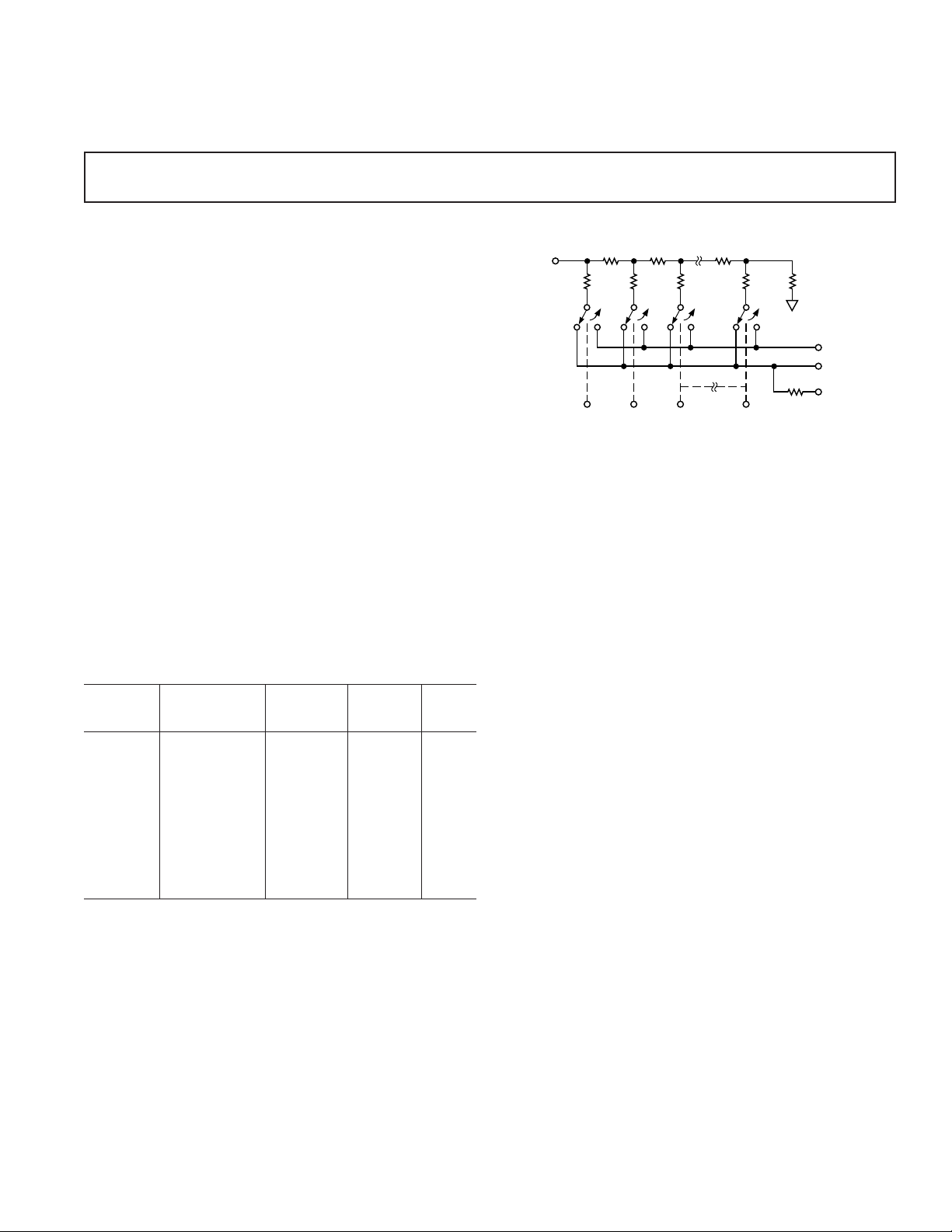
10kΩ 10kΩ 10kΩ
20kΩ 20kΩ 20kΩ 20kΩ 20kΩ
S1 S2 S3 S12
V
REF
OUT2
OUT1
R
FEEDBACK
BIT 12 (LSB)BIT 3BIT 2BIT 1 (MSB)
DIGITAL INPUTS (DTL/TTL/CMOS COMPATIBLE)
LOGIC: A SWITCH IS CLOSED TO I
OUT1
FOR
ITS DIGITAL INPUT IN A "HIGH" STATE.
10kΩ
a
12-Bit Monolithic Multiplying DAC
AD7541A
FEATURES
Improved Version of AD7541
Full Four-Quadrant Multiplication
12-Bit Linearity (Endpoint)
All Parts Guaranteed Monotonic
TTL/CMOS Compatible
Low Cost
Protection Schottky Diodes Not Required
Low Logic Input Leakage
GENERAL DESCRIPTION
The Analog Devices AD7541A is a low cost, high performance
12-bit monolithic multiplying digital-to-analog converter. It is
fabricated using advanced, low noise, thin film on CMOS
technology and is available in a standard 18-lead DIP and in
20-terminal surface mount packages.
The AD7541A is functionally and pin compatible with the industry standard AD7541 device and offers improved specifications and performance. The improved design ensures that the
device is latch-up free so no output protection Schottky diodes
are required.
This new device uses laser wafer trimming to provide full 12-bit
endpoint linearity with several new high performance grades.
ORDERING GUIDE
2
Model
AD7541AJN 0°C to +70°C ±1 LSB ±6 LSB N-18
AD7541AKN 0°C to +70°C ±1/2 LSB ±1 LSB N-18
AD7541AJP 0°C to +70°C ±1 LSB ±6 P-20A
AD7541AKP 0°C to +70°C ±1/2 LSB ±1 P-20A
AD7541AKR 0°C to +70°C ±1/2 LSB ±1 R-18
AD7541AAQ –25°C to +85°C ±1 LSB ±6 LSB Q-18
AD7541ABQ –25°C to +85°C ±1/2 LSB ±1 LSB Q-18
AD7541ASQ –55°C to +125°C ± 1 LSB ±6 LSB Q-18
AD7541ATQ –55°C to +125°C ±1/2 LSB ±1 LSB Q-18
AD7541ASE –55°C to +125°C ±1 LSB ±6 LSB E-20A
AD7541ATE –55°C to +125°C ±1/2 LSB ±1 LSB E-20A
NOTES
1
Analog Devices reserves the right to ship either ceramic (D-18) or cerdip (Q-18)
hermetic packages.
2
To order MIL-STD-883, Class B process parts, add /883B to part number. Contact
local sales office for military data sheet.
3
E = Leadless Ceramic Chip Carrier; N = Plastic DIP; P = Plastic Leaded Chip
Carrier; Q = Cerdip; R = Small Outline IC.
Temperature Accuracy Error Package
Range T
Relative Gain
to T
MIN
1
= +258C Options
MAXTA
PRODUCT HIGHLIGHTS
Compatibility: The AD7541A can be used as a direct replace-
ment for any AD7541-type device. As with the Analog Devices
AD7541, the digital inputs are TTL/CMOS compatible and
have been designed to have a ± 1 µA maximum input current
requirement so as not to load the driving circuitry.
Improvements: The AD7541A offers the following improved
specifications over the AD7541:
1. Gain Error for all grades has been reduced with premium
grade versions having a maximum gain error of ±3 LSB.
2. Gain Error temperature coefficient has been reduced to
3
2 ppm/°C typical and 5 ppm/°C maximum.
3. Digital-to-analog charge injection energy for this new device
is typically 20% less than the standard AD7541 part.
4. Latch-up proof.
5. Improvements in laser wafer trimming provides 1/2 LSB max
differential nonlinearity for top grade devices over the operating temperature range (vs. 1 LSB on older 7541 types).
6. All grades are guaranteed monotonic to 12 bits over the
operating temperature range.
FUNCTIONAL BLOCK DIAGRAM
REV. B
Information furnished by Analog Devices is believed to be accurate and
reliable. However, no responsibility is assumed by Analog Devices for its
use, nor for any infringements of patents or other rights of third parties
which may result from its use. No license is granted by implication or
otherwise under any patent or patent rights of Analog Devices.
One Technology Way, P.O. Box 9106, Norwood, MA 02062-9106, U.S.A.
Tel: 617/329-4700 World Wide Web Site: http://www.analog.com
Fax: 617/326-8703 © Analog Devices, Inc., 1997

AD7541A–SPECIFICATIONS
(VDD = +15 V, V
TA =T
Parameter Version +258CT
= +10 V; OUT 1 = OUT 2 = GND = 0 V unless otherwise noted)
REF
=
A
MIN, TMAX
1
Units Test Conditions/Comments
ACCURACY
Resolution All 12 12 Bits
Relative Accuracy J, A, S ±1 ±1 LSB max ±1 LSB = ±0.024% of Full Scale
K, B, T ±1/2 ±1/2 LSB max ±1/2 LSB = ±0.012% of Full Scale
Differential Nonlinearity J, A, S ±1 ±1 LSB max All Grades Guaranteed Monotonic
to T
K, B, T ±1/2 ±1/2 LSB max to 12 Bits, T
MIN
Gain Error J, A, S ±6 ± 8 LSB max Measured Using Internal R
MAX
.
and Includes
FB
K, B, T ±3 ±5 LSB max Effect of Leakage Current and Gain TC.
Gain Temperature Coefficient
2
Gain Error Can Be Trimmed to Zero.
DGain/DTemperature All 5 5 ppm/°C max Typical Value Is 2 ppm/°C.
Output Leakage Current
OUT1 (Pin 1) J, K ±5 ±10 nA max All Digital Inputs = 0 V.
A, B ±5 ±10 nA max
S, T ±5 ±200 nA max
OUT2 (Pin 2) J, K ±5 ±10 nA max All Digital Inputs = V
DD
.
A, B ±5 ±10 nA max
S, T ±5 ±200 nA max
REFERENCE INPUT
Input Resistance (Pin 17 to GND) All 7–18 7–18 kΩ min/max Typical Input Resistance = 11 kΩ.
Typical Input Resistance Temperature
Coefficient = –300 ppm/°C.
DIGITAL INPUTS
V
(Input HIGH Voltage) All 2.4 2.4 V min
IH
V
(Input LOW Voltage) All 0.8 0.8 V max
IL
I
(Input Current) All ±1 ±1 µA max Logic Inputs Are MOS Gates. IIN typ (25°C) = 1 nA.
IN
CIN (Input Capacitance)
2
All 8 8 pF max VIN = 0 V
POWER SUPPLY REJECTION
DGain/DV
DD
All ±0.01 ±0.02 % per % max DVDD = ±5%
POWER SUPPLY
V
Range All +5 to +16 +5 to +16 V min/V max Accuracy Is Not Guaranteed Over This Range.
DD
I
DD
All 2 2 mA max All Digital Inputs VIL or VIH.
100 500 µA max All Digital Inputs 0 V or VDD.
AC PERFORMANCE CHARACTERISTICS
These Characteristics are included for Design Guidance only and are not subject to test. VDD = +15 V, VIN = +10 V except where noted,
OUT1 = 0UT2 = GND = 0 V, Output Amp is AD544 except where noted.
TA =T
Parameter Version1+258CT
PROPAGATION DELAY (From Digital Input OUT 1 Load = 100 Ω, C
Change to 90% of Final Analog Output) All 100 — ns typ Digital Inputs = 0 V to VDD or VDD to 0 V.
DIGITAL TO ANALOG GLITCH V
IMPULSE V
All 1000 — nV-sec typ Measured using Model 50K as output amplifier.
MULTIPLYING FEEDTHROUGH ERROR
(V
to OUT1) All 1.0 — mV p-p typ V
REF
3
OUTPUT CURRENT SETTLING TIME All 0.6 — µs typ To 0.01% of full-scale range.
OUTPUT CAPACITANCE
C
(Pin 1) All 200 200 pF max Digital Inputs
OUT1
C
(Pin 2) All 70 70 pF max = V
OUT2
C
(Pin 1) All 70 70 pF max Digital Inputs
OUT1
C
(Pin 2) All 200 200 pF max = V
OUT2
NOTES
1
Temperature range as follows: J, K versions, 0°C to +70°C; A, B versions, –25°C to +85°C; S, T versions, –55°C to +125°C.
2
Guaranteed by design but not production tested.
3
To minimize feedthrough in the ceramic package (Suffix D) the user must ground the metal lid.
Specifications subject to change without notice.
=
A
MIN, TMAX
1
Units Test Conditions/Comments
= 0 V. All digital inputs 0 V to VDD or
REF
to 0 V.
DD
= ±10 V, 10 kHz sine wave.
REF
OUT 1 Load = 100 Ω, C
Digital Inputs = 0 V to VDD or VDD to 0 V.
IH
IL
= 13 pF.
EXT
= 13 pF.
EXT
–2– REV. B

AD7541A
WARNING!
ESD SENSITIVE DEVICE
ABSOLUTE MAXIMUM RATINGS*
(T
= +25°C unless otherwise noted)
A
to GND . . . . . . . . . . . . . . . . . . . . . . . . . . . . . . . . +17 V
V
DD
to GND . . . . . . . . . . . . . . . . . . . . . . . . . . . . . . . . ±25 V
V
REF
to GND . . . . . . . . . . . . . . . . . . . . . . . . . . . . . . . . . ±25 V
V
RFB
Digital Input Voltage to GND . . . . . . . . –0.3 V, V
OUT 1, OUT 2 to GND . . . . . . . . . . . . –0.3 V, V
+ 0.3 V
DD
+ 0.3 V
DD
Power Dissipation (Any Package)
To +75°C . . . . . . . . . . . . . . . . . . . . . . . . . . . . . . . 450 mW
Derates above +75°C . . . . . . . . . . . . . . . . . . . . . . 6 mW/°C
Operating Temperature Range
Commercial (J, K Versions) . . . . . . . . . . . . . 0°C to +70°C
Industrial (A, B Versions) . . . . . . . . . . . . . –25°C to +85°C
Extended (S, T Versions) . . . . . . . . . . . . . –55°C to +125°C
Storage Temperature . . . . . . . . . . . . . . . . . . –65°C to +150°C
Lead Temperature (Soldering, 10 secs) . . . . . . . . . . . +300°C
*Stresses above those listed under Absolute Maximum Ratings may cause perma-
nent damage to the device. This is a stress rating only; functional operation of the
device at these or any other conditions above those indicated in the operational
sections of this specification is not implied. Exposure to absolute maximum rating
conditions for extended periods may affect device reliability.
CAUTION
ESD (electrostatic discharge) sensitive device. Electrostatic charges as high as 4000 V readily
accumulate on the human body and test equipment and can discharge without detection.
Although the AD7541A features proprietary ESD protection circuitry, permanent damage may
occur on devices subjected to high energy electrostatic discharges. Therefore, proper ESD
precautions are recommended to avoid performance degradation or loss of functionality.
TERMINOLOGY
RELATIVE ACCURACY
Relative accuracy or endpoint nonlinearity is a measure of the
OUTPUT LEAKAGE CURRENT
Current which appears at OUTI with the DAC loaded to all 0s
or at OUT2 with the DAC loaded to all 1s.
maximum deviation from a straight line passing through the
endpoints of the DAC transfer function. It is measured after
adjusting for zero and full scale and is expressed in % of fullscale range or (sub)multiples of 1 LSB.
MULTIPLYING FEEDTHROUGH ERROR
AC error due to capacitive feedthrough from V
OUT1 with DAC loaded to all 0s.
terminal to
REF
DIFFERENTIAL NONLINEARITY
Differential nonlinearity is the difference between the measured
change and the ideal l LSB change between any two adjacent
codes. A specified differential nonlinearity of ±1 LSB max over
OUTPUT CURRENT SETTLING TIME
Time required for the output function of the DAC to settle to
within 1/2 LSB for a given digital input stimulus, i.e., 0 to full
scale.
the operating temperature range insures monotonicity.
PROPAGATION DELAY
GAIN ERROR
Gain error is a measure of the output error between an ideal
DAC and the actual device output. For the AD7541A, ideal
This is a measure of the internal delay of the circuit and is measured from the time a digital input changes to the point at which
the analog output at OUT1 reaches 90% of its final value.
maximum output is
4095
(V
–
4096
REF
).
Gain error is adjustable to zero using external trims as shown in
Figures 4, 5 and 6.
DIGITAL-TO-ANALOG CHARGE INJECTION (QDA)
This is a measure of the amount of charge injected from the
digital inputs to the analog outputs when the inputs change
state. It is usually specified as the area of the glitch in nV secs
and is measured with V
= GND and a Model 50K as the
REF
output op amp, C1 (phase compensation) = 0 pF.
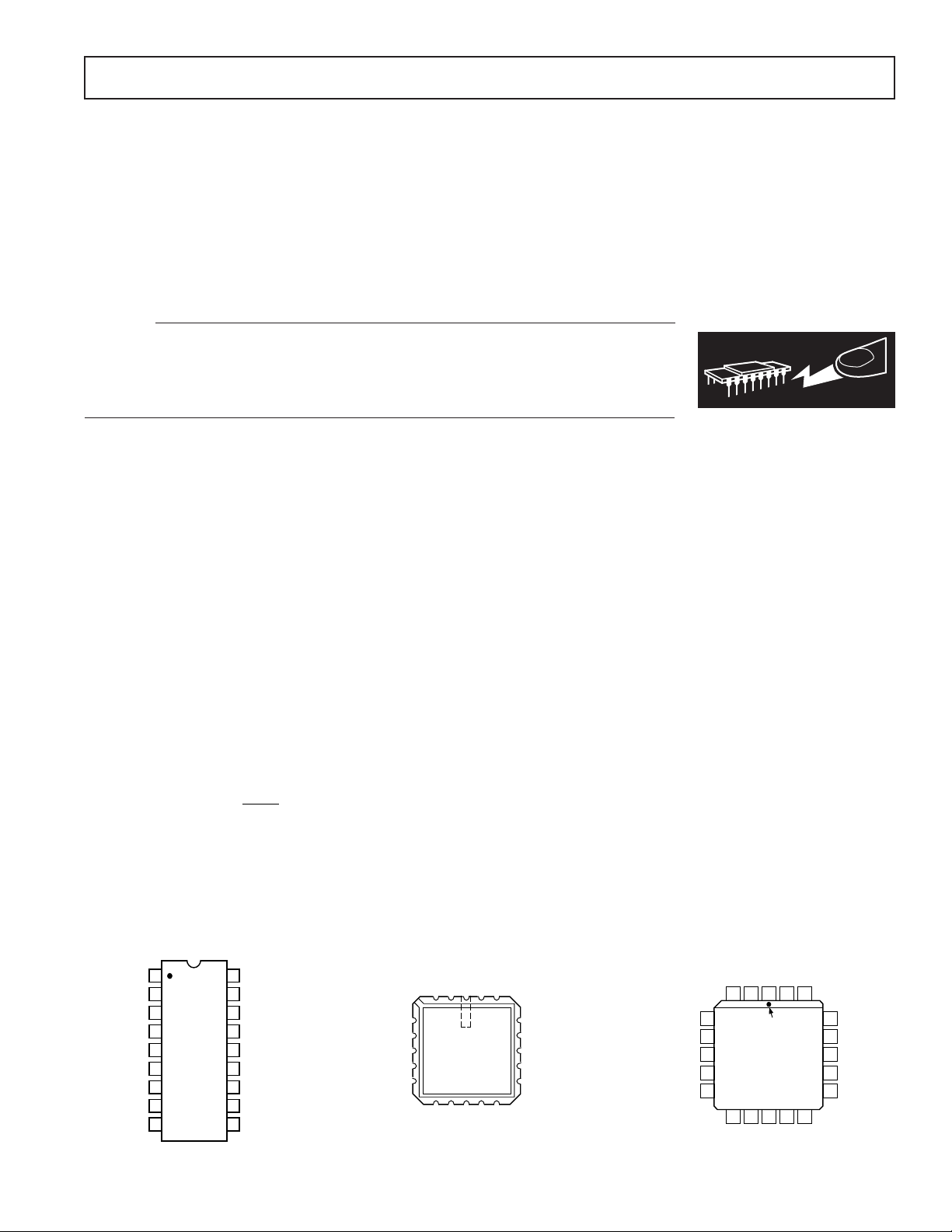
PIN CONFIGURATIONS
DIP/SOIC LCCC PLCC
FB
OUT1
OUT2
GND
BIT 1 (MSB)
BIT 2
BIT 3
BIT 4
BIT 5
BIT 6
1
2
3
4
AD7541A
5
TOP VIEW
(Not to Scale)
6
7
8
9
18
R
FEEDBACK
V
17
REF
16
VDD (+)
15
BIT 12 (LSB)
BIT 11
14
BIT 10
13
12
BIT 9
11
BIT 8
BIT 7
10
OUT 1
IN
4
GND
BIT 2
BIT 3
BIT 4
5
6
7
8
BIT 1 (MSB)
NC = NO CONNECT
20 19123
AD7541A
TOP VIEW
(Not to Scale)
910111213
NC
BIT 7
BIT 5
BIT 6
BIT 8
18
V
DD
17
BIT 12 (LSB)
16
BIT 11
15
BIT 10
14
BIT 9
GND
BIT 1 (MSB)
BIT 2
BIT 3
BIT 4
NC = NO CONNECT
OUT 2
4
5
6
7
8
9101112
BIT 5
AD7541A
(Not to Scale)
REF
R
OUT 2
NC
V
NC
OUT 1
20 19
123
PIN 1
IDENTIFIER
TOP VIEW
BIT 6NCBIT 7
FB
REF
R
V
13
BIT 8
18
V
BIT 12 (LSB)
17
BIT 11
16
15
BIT 10
BIT 9
14
DD
–3–REV. B
 Loading...