LC2MOS
V
V
Microprocessor-Compatible 14-Bit DAC
FEATURES
All grades 14-bit monotonic over the full temperature range
Low cost, 14-bit upgrade for 12-bit systems
14-bit parallel load with double buffered inputs
Small 24-pin, 0.30” DIP and SOIC
Low output leakage (<20 nA) over the full temperature range
APPLICATIONS
Microprocessor-based control systems
Digital audio
Precision servo control
Control and measurement in high temperature environments
GENERAL DESCRIPTION
The AD7538 is a 14-bit monolithic CMOS digital-to-analog
converter (DAC) that uses laser trimmed thin-film resistors to
achieve excellent linearity.
The DAC is loaded by a single 14-bit wide word using standard
chip select and memory write logic. Double buffering, which is
optional using
containing multiple AD7538s.
A novel low leakage configuration enables the AD7538 to
exhibit excellent output leakage current characteristics over
the specified temperature range.
The AD7538 is manufactured using the linear-compatible
CMOS (LC
microprocessors and accepts TTL or CMOS logic level inputs.
LDAC
, allows simultaneous updates in a system
2
MOS) process. It is speed compatible with most
AD7538
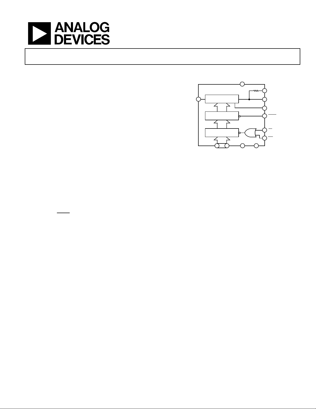
FUNCTIONAL BLOCK DIAGRAM
DD
23
AD7538
14-BIT DAC
1
REF
DAC REGISTER
INPUT
REGISTER
14
619
DB13 TO DB0 DGND
Figure 1.
PRODUCT HIGHLIGHTS
1. Guaranteed Monotonicity.
The AD7538 is guaranteed monotonic to 14-bits over the
full temperature range for all grades.
2. Low Cost.
The AD7538, with its 14-bit dynamic range, affords a low
cost solution for 12-bit system upgrades.
3. Small Package Size.
The AD7538 is packaged in a small 24-pin, 0.3" DIP and a
24-pin SOIC.
4. Low Output Leakage.
By tying V
achieve a low output leakage current at high temperatures.
5. Wide Power Supply Tolerance.
The device operates on a +12 V to +15 V V
tolerance on this nominal figure. All specifications are
guaranteed over this range.
(Pin 24) to a negative voltage, it is possible to
SS
2
R
FB
3
I
OUT
4
AGND
20
LDAC
21
CS
22
WR
245
V
SS
, with a ±5%
DD
01139-001
Rev. B
Information furnished by Analog Devices is believed to be accurate and reliable. However, no
responsibility is assumed by Analog Devices for its use, nor for any infringements of patents or other
rights of third parties that may result from its use. Specifications subject to change without notice. No
license is granted by implication or otherwise under any patent or patent rights of Analog Devices.
Trademarks and registered trademarks are the property of their respective owners.
One Technology Way, P.O. Box 9106, Norwood, MA 02062-9106, U.S.A.
Tel: 781.329.4700 www.analog.com
Fax: 781.461.3113 ©2009 Analog Devices, Inc. All rights reserved.

AD7538
TABLE OF CONTENTS
Features .............................................................................................. 1
Applications ....................................................................................... 1
Functional Block Diagram .............................................................. 1
General Description ......................................................................... 1
Product Highlights ........................................................................... 1
Revision History ............................................................................... 2
Specifications ..................................................................................... 3
AC Performance Characteristics ................................................ 4
Timing Characteristics ................................................................ 4
Timing Diagram ........................................................................... 5
Absolute Maximum Ratings ............................................................ 6
ESD Caution .................................................................................. 6
Pin Configuration and Function Descriptions ............................. 7
Terminology ...................................................................................... 8
DAC Section ...................................................................................... 9
Circuit Information ........................................................................ 10
Equivalent Circuit Analysis ...................................................... 10
Digital Section ............................................................................ 10
Unipolar Binary Operation (2-Quadrant Multiplication) .... 10
Bipolar Operation (4-Quadrant Multiplication) .................... 11
Low Leakage Configuration ...................................................... 11
Programmable Gain Amplifier ................................................. 12
Application Hints ........................................................................... 13
Output Offset .............................................................................. 13
General Ground Management .................................................. 13
Microprocessor Interfacing ....................................................... 13
AD7538-to-8086 Interface ........................................................ 13
AD7538-to-MC68000 Interface ............................................... 13
Digital Feedthrough ................................................................... 14
Outline Dimensions ....................................................................... 15
Ordering Guide .......................................................................... 16
REVISION HISTORY
1/09—Rev. A to Rev. B
Updated Format .................................................................. Universal
Changes to Table 1 ............................................................................ 3
Updated Outline Dimensions ....................................................... 15
Changes to Ordering Guide .......................................................... 15
5/87—Rev. 0 to Rev. A
Rev. B | Page 2 of 16

AD7538
SPECIFICATIONS
VDD = 11.4 V to 15.75 V1, V
Table 1.
Parameter2
ACCURACY
Resolution 14 14 14 14 Bits
Relative Accuracy ±2 ±1 ±2 ±1 LSB max
Differential Nonlinearity ±1 ±1 ±1 ±1 LSB max Over temperature
Full-Scale Error Measured using internal RFB DAC
+25°C ±4 ±4 ±4 ±4 LSB max Registers loaded with all 1s
T
to T
MIN
±8 ±5 ±10 ±6 LSB max
MAX
Gain Temperature Coefficient3;
ΔGain/ΔTemperature
Output Leakage Current
(Pin 3)
I
OUT
25°C ±5 ±5 ±5 ±5 nA max All digital inputs 0 V
T
to T
MIN
T
MIN
±10 ±10 ±20 ±20 nA max VSS = –300 mV
MAX
to T
±25 ±25 ±150 ±150 nA max VSS = 0 V
MAX
REFERENCE INPUT
Input Resistance (Pin 1) 3.5 3.5 3.5 3.5 kΩ min Typical input resistance = 6 kΩ
10 10 10 10 kΩ max
DIGITAL INPUTS
VIH (Input High Voltage) 2.4 2.4 2.4 2.4 V min
VIL (Input Low Voltage) 0.8 0.8 0.8 0.8 V max
IIN (Input Current)
25°C ±1 ±1 ±1 ±1 μA max VIN = 0 V or VDD
T
to T
MIN
±10 ±10 ±10 ±10 μA max
MAX
CIN (Input Capacitance)3 7 7 7 7 pF max
POWER SUPPLY
VDD Range 11.4/15.75 11.4/15.75 11.4/15.75 11.4/15.75 V min/V max
VSS Range −200/−500 −200/−500 −200/−500 −200/−500
IDD 4 4 4 4 mA max All digital inputs are VIL or V
500 500 500 500 μA max All digital inputs are 0 V or V
1
Specifications are guaranteed for a VDD of 11.4 V to 15.75 V. At VDD = 5 V, the device is fully functional with degraded specifications.
2
Temperature range as follows: J, K Versions: 0°C to +70°C
3
Sample tested to ensure compliance.
= 10 V; V
REF
A, J
Versions
PIN3
= V
PIN4
B, K
Versions S Version T Version Unit Test Conditions/Comments
±2 ±2 ±2 ±2 ppm/°C typ
A, B Versions: −25°C to +85°C
S, T Versions: −55°C to +125°C
= 0 V, VSS = −300 mV; all specifications T
to T
MIN
mV min/
mV max
, unless otherwise noted.
MAX
All grades guaranteed
monotonic
Specification guaranteed over
this range
Specification guaranteed over
this range
IH
DD
Rev. B | Page 3 of 16

AD7538
AC PERFORMANCE CHARACTERISTICS
These characteristics are included for design guidance only and are not subject to test. VDD = 11.4 V to 15.75 V, V
0 V, V
= 0 V or −300 mV, output amplifier is AD711 except where noted.
SS
Table 2.
T
= 25°C
A
Parameter
TA = T
MIN
, T
MAX
Unit Test Conditions/Comments
Output Current Settling Time 1.5 μs max To 0.003% of full-scale range
load= 100 Ω, C
I
OUT
= 13 pF DAC register alternately loaded
EXT
with all 1s and all 0s; typical value of settling time is 0.8 μs
Digital-to-Analog Glitch Impulse 20 nV-sec typ
Measured with V
REF
= 0 V. I
load = 100 Ω, C
OUT
register alternately loaded with all 1s and all 0s
Multiplying Feedthrough Error 3 5 mV p-p typ V
= ±10 V, 10 kHz sine wave DAC
REF
Register loaded with all 0s
Power Supply Rejection
ΔGain/ΔVDD ±0.01 ±0.02 % per % max ΔVDD = ±5%
Output Capacitance
C
(Pin 3) 260 260 pF max DAC register loaded with all 1s
OUT
C
(Pin 3) 130 130 pF max DAC register loaded with all 0s
OUT
Output Noise Voltage Density
(10 Hz to 100 kHz) 15 nV√Hz typ Measured between RFB and I
OUT
= 10 V, V
REF
= V
PIN3
= 13 pF; DAC
EXT
PIN4
=
TIMING CHARACTERISTICS
VDD = 11.4 V to 15.75 V, V
Figure 2 for a timing diagram.
Table 3.
Limit at
T
Parameter1
t1
t2
t3
= +25°C
A
0 0 0 ns min
0 0 0 ns min
170 200 240 ns min
t4 170 200 240 ns min Write pulse width
t5 140 160 180 ns min Data setup time
t6
1
Temperature range as follows: J, K Versions: 0°C to +70°C
20 20 30 ns min Data hold time
= 10 V, V
REF
PIN3
= V
PIN4
Limit at TA = 0°C to +70°C
TA = −25°C to +85°C
A, B Versions: −25°C to +85°C
S, T Versions: −55°C to +125°C
= 0 V, VSS = 0 V or −300 mV. All specifications T
Limit at
TA = −55°C to +125°C
Unit Test Conditions/Comments
MIN
to T
unless otherwise noted. See
MAX
to WR setup time
CS
CS to WR hold time
LDAC
pulse width
Rev. B | Page 4 of 16

AD7538
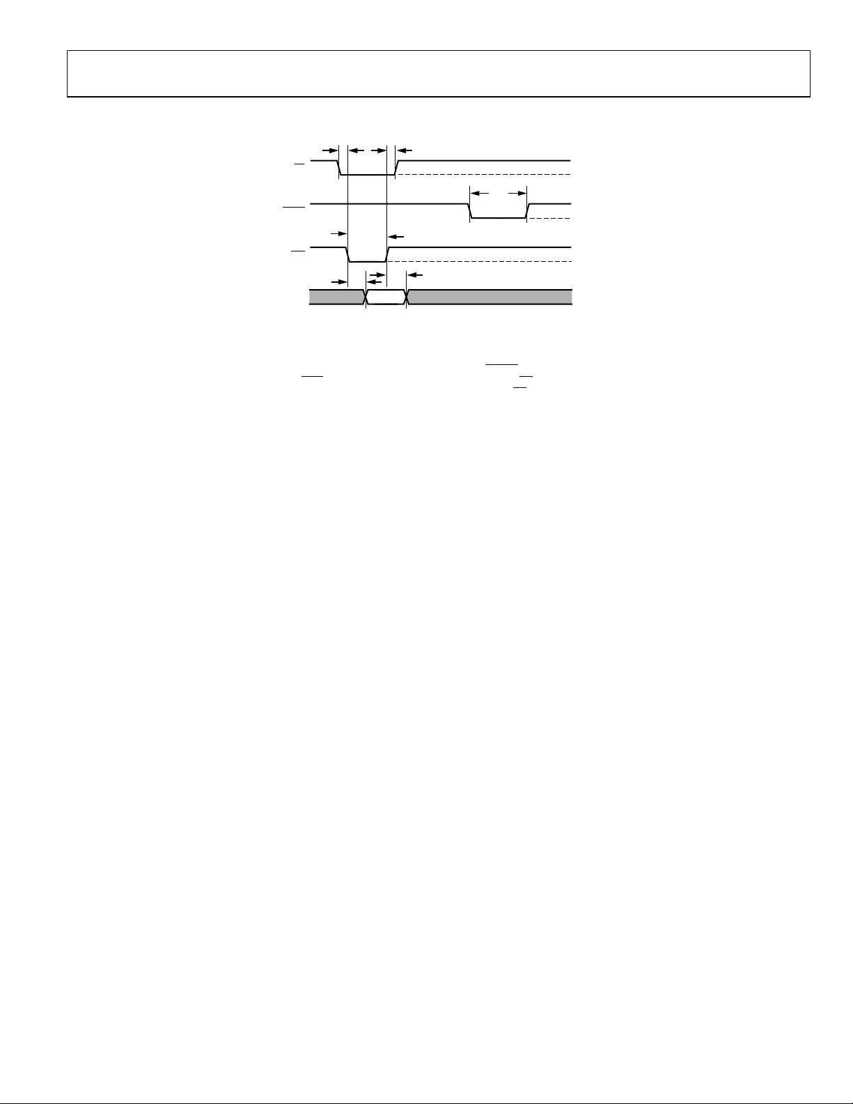
TIMING DIAGRAM
t
1
CS
LDAC
WR
DATA
NOTES
1. ALL INP UT SIGNAL RISE AND FALL TIMES MEASURES FROM 10%
TO 90% OF 5V,
2. TIMING MEASUREMENT REFERENCE LEVEL IS .
3. IF LDAC I S ACTIVATED PRIOR TO THE RISI NG EDGE O F WR,
THEN IT MUST STAY LOW FOR
t
2
t
4
t
t
t
6
5
=
t
= 20ns.
R
F
t
3
Figure 2. Timing Diagram
t
3
+ V
V
IH
IL
2
OR LONGE R AFTER WR GOES HIGH.
5V
0V
5V
0V
5V
0V
5V
0V
01139-002
Rev. B | Page 5 of 16
 Loading...