LC2MOS
a
FEATURES
All Grades 14-Bit Monotonic Over the Full Temperature
Range
Low Cost 14-Bit Upgrade for 12-Bit Systems
14-Bit Parallel Load with Double Buffered Inputs
Small 24-Pin, 0.30 DIP and SOIC
Low Output Leakage (<20 nA) Over the Full
Temperature Range
APPLICATIONS
Microprocessor Based Control Systems
Digital Audio
Precision Servo Control
Control and Measurement in High Temperature
Environments
GENERAL DESCRIPTION
The AD7538 is a 14-bit monolithic CMOS D/A converter
which uses laser trimmed thin-film resistors to achieve excellent
linearity.
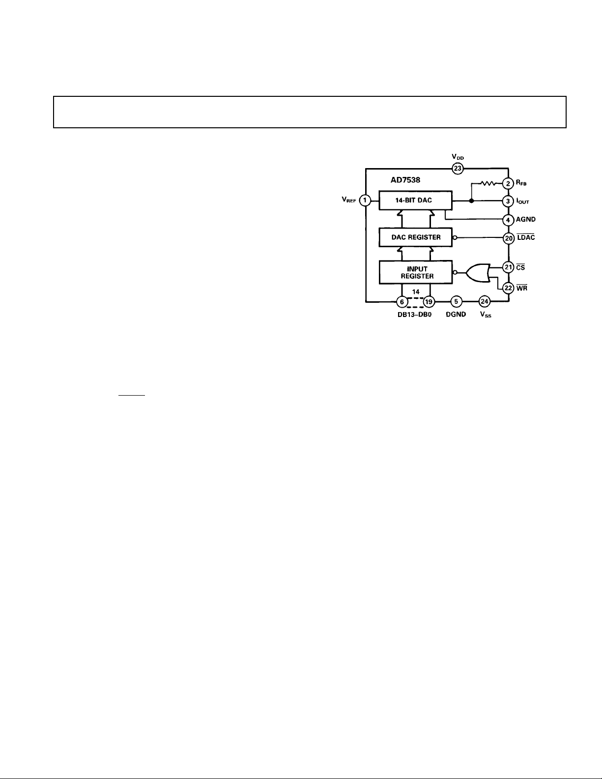
The DAC is loaded by a single 14-bit wide word using standard
Chip Select and Memory Write Logic. Double buffering, which
is optional using
tem containing multiple AD7538s.
A novel low leakage configuration (U.S. Patent No. 4,590,456)
enables the AD7538 to exhibit excellent output leakage current
characteristics over the specified temperature range.
The AD7538 is manufactured using the Linear Compatible
CMOS (LC
microprocessors and accepts TTL or CMOS logic level inputs.
LDAC, allows simultaneous update in a sys-
2
MOS) process. It is speed compatible with most
mP-Compatible 14-Bit DAC
AD7538
FUNCTIONAL BLOCK DIAGRAM
PRODUCT HIGHLIGHTS
1. Guaranteed Monotonicity
The AD7538 is guaranteed monotonic to 14-bits over the
full temperature range for all grades.
2. Low Cost
The AD7538, with its 14-bit dynamic range, affords a low
cost solution for 12-bit system upgrades.
3. Small Package Size
The AD7538 is packaged in a small 24-pin, 0.3" DIP and a
24-pin SOIC.
4. Low Output Leakage
By tying V
achieve a low output leakage current at high temperatures.
5. Wide Power Supply Tolerance
The device operates on a +12 V to +15 V V
tolerance on this nominal figure. All specifications are
guaranteed over this range.
(Pin 24) to a negative voltage, it is possible to
SS
, with a ±5%
DD
REV. A
Information furnished by Analog Devices is believed to be accurate and
reliable. However, no responsibility is assumed by Analog Devices for its
use, nor for any infringements of patents or other rights of third parties
which may result from its use. No license is granted by implication or
otherwise under any patent or patent rights of Analog Devices.
One Technology Way, P.O. Box 9106, Norwood, MA 02062-9106, U.S.A.
Tel: 617/329-4700 Fax: 617/326-8703

(VDD = +11.4 V to +15.75 V2, V
AD7538–SPECIFICA TIONS
Parameter Versions Versions S Version T Version Units Test Conditions/Comments
ACCURACY
Resolution 14 14 14 14 Bits
Relative Accuracy ± 2 ±1 ± 2 ±1 LSB max All Grades Guaranteed Monotonic
Differential Nonlinearity ±1 ±1 ±1 ±1 LSB max Over Temperature.
Full-Scale Error Measured Using Internal R
+25°C ±4 ±4 ±4 ±4 LSB max Registers Loaded with All 1s.
T
to T
MIN
MIN
MIN
MIN
to T
to T
to T
MAX
MAX
MAX
MAX
3
OUT
(Pin 3)
Gain Temperature Coefficient3;
∆Gain/∆Temperature ± 2 ±2 ±2 ± 2 ppm/°C typ
Output Leakage Current I
+25°C ±5 ±5 ±5 ±5 nA max All Digital Inputs 0 V
T
T
REFERENCE INPUT
Input Resistance, Pin 1 3.5 3.5 3.5 3.5 k Ω min Typical Input Resistance = 6 kΩ
DIGITAL INPUTS
VIH (Input High Voltage) 2.4 2.4 2.4 2.4 V min
VIL (Input Low Voltage) 0.8 0.8 0.8 0.8 V max
IIN (Input Current)
+25°C ±1 ±1 ±1 ±1 µA max VIN = 0 V or V
T
CIN (Input Capacitance)
J, K A, B
±8 ±5 ±10 ±6 LSB max
±10 ±10 ±20 ±20 nA max VSS = –300 mV
±25 ±25 ±150 ±150 nA max VSS = 0 V
10 10 10 10 kΩ max
±10 ±10 ±10 ±10 µA max
7 7 7 7 pF max
1
VSS = –300 mV. All specifications T
= +10 V; V
REF
MIN
= V
PIN3
PIN4
to T
unless otherwise noted.)
MAX
= 0 V,
FB
DD
DAC
POWER SUPPLY
VDD Range 11.4/15.75 11.4/15.75 11.4/15.75 11.4/15.75 V min/V max Specification Guaranteed Over
VSS Range –200/–500 –200/–500 –200/–500 –200/–500 mV min/mV max This Range
I
DD
4 4 4 4 mA max All Digital Inputs VIL or V
500 500 500 500 µA max All Digital Inputs 0 V or V
These characteristics are included for Design Guidance only and are not sub-
AC PERFORMANCE CHARACTERISTICS
Parameter TA = +258C TA = T
MIN
ject to test. (VDD = +11.4 V to +15.75 V, V
O V or –300 mV, Output Amplifier is AD711 except where noted.)
, T
MAX
Units Test Conditions/Comments
= +10 V, V
REF
PIN3
= V
= O V, VSS =
PIN4
Output Current Settling Time 1.5 µs max To 0.003% of Full-Scale Range.
I
Load= 100 Ω, C
OUT
= 13 pF.
EXT
DAC Register Alternately Loaded
with All 1s and All 0s. Typical Value
of Settling Time Is 0.8 µs.
Digital to Analog Glitch Impulse 20 nV-sec typ Measured with V
= 100 Ω, C
EXT
= 0 V. I
REF
OUT
Load
= 13 pF. DAC Register
Alternately Loaded with All 1s and All 0s.
Multiplying Feedthrough Error 3 5 mV p-p typ V
= ± 10 V, 10 kHz Sine Wave DAC
REF
Register Loaded with All 0s.
Power Supply Rejection
∆Gain/∆V
DD
±0.01 ±0.02 % per % max ∆VDD = ±5%
Output Capacitance
C
(Pin 3) 260 260 pF max DAC Register Loaded with All 1s
OUT
C
(Pin 3) 130 130 pF max DAC Register Loaded with All 0s
OUT
Output Noise Voltage Density
(10 Hz–100 kHz) 15 nV√Hz typ Measured Between RFB and I
NOTES
Temperature range as follows: J, K Versions: 0°C to +70°C
2
Specifications are guaranteed for a VDD of +11.4 V to +15.75 V. At VDD = 5 V, the device is fully functional with degraded specifications.
3
Sample tested to ensure compliance.
Specifications subject to change without notice.
A, B Versions: –25°C to +85°C
S, T Versions: –55°C to +125°C
OUT
IH
DD
–2–
REV. A

AD7538
WARNING!
ESD SENSITIVE DEVICE
(VDD = +11.4 V to +15.75 V, V
1
TIMING CHARACTERISTICS
All specifications T
MIN
Limit at
Limit at T
Parameter TA = +258CT
t
1
t
2
t
3
t
4
t
5
t
6
NOTES
1
Temperature range as follows: J, K Versions: 0°C to +70°C
Specifications subject to change without notice.
0 0 0 ns min CS to WR Setup Time
0 0 0 ns min CS to WR Hold Time
170 200 240 ns min LDAC Pulse Width
170 200 240 ns min Write Pulse Width
140 160 180 ns min Data Setup Time
20 20 30 ns min Data Hold Time
A, B Versions: –25°C to +85°C
S, T Versions: –55°C to +125°C
= 08C to +708C Limit at
A
= –258C to +858CTA = –558C to +1258C Units Test Conditions/Comments
A
ABSOLUTE MAXIMUM RATINGS*
(TA= +25°C unless otherwise stated)
VDD (Pin 23) to DGND . . . . . . . . . . . . . . . . . . .–0.3 V, +17 V
V
(Pin 24) to AGND . . . . . . . . . . . . . . . . . . .–15 V, +0.3 V
SS
V
(Pin 1) to AGND . . . . . . . . . . . . . . . . . . . . . . . . . ±25 V
REF
V
(Pin 2) to AGND . . . . . . . . . . . . . . . . . . . . . . . . .±25 V
RFB
Digital Input Voltage (Pins 6–22)
to DGND . . . . . . . . . . . . . . . . . . . . . . . –0.3 V, V
V
to DGND . . . . . . . . . . . . . . . . . . . . –0.3 V, VDD +0.3 V
PIN3
AGND to DGND . . . . . . . . . . . . . . . . . . –0.3 V, V
+0.3 V
DD
+0.3 V
DD
Power Dissipation (Any Package)
To +75°C . . . . . . . . . . . . . . . . . . . . . . . . . . . . . . . 1000 mW
Derates Above +75°C . . . . . . . . . . . . . . . . . . . . 10 mW/°C
= +10 V, V
REF
to T
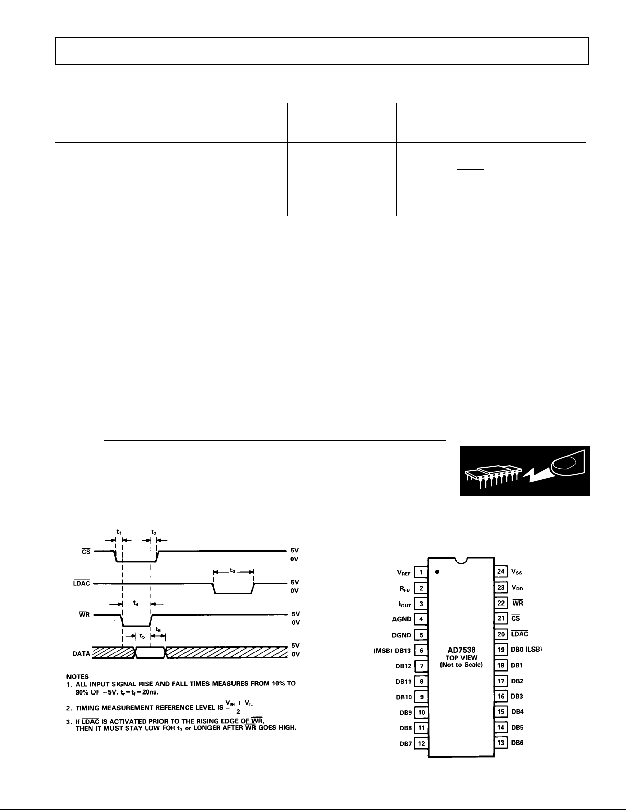
unless otherwise noted. See Figure 1 for Timing Diagram.)
MAX
PIN3
= V
= 0 V, VSS = 0 V or –300 mV.
PIN4
Operating Temperature Range
Commercial (J, K Versions) . . . . . . . . . . . . . .0°C to +70°C
Industrial (A, B Versions) . . . . . . . . . . . . . . –25°C to +85°C
Extended (S, T Versions) . . . . . . . . . . . . . –55°C to +125°C
Storage Temperature . . . . . . . . . . . . . . . . –65°C to +150°C
Lead Temperature (Soldering, 10 sec) . . . . . . . . . . . . +300°C
*Stresses above those listed under “Absolute Maximum Ratings” may cause
permanent damage to the device. This is a stress rating only and functional
operation of the device at these or any other conditions above those indicated in
the operational sections of this specification is not implied. Exposure to absolute
maximum rating conditions for extended periods may affect device reliability.
CAUTION
ESD (electrostatic discharge) sensitive device. Electrostatic charges as high as 4000 V readily
accumulate on the human body and test equipment and can discharge without detection.
Although the AD7538 features proprietary ESD protection circuitry, permanent damage may
occur on devices subjected to high energy electrostatic discharges. Therefore, proper ESD
precautions are recommended to avoid performance degradation or loss of functionality.
PIN CONFIGURATION
DIP, SOIC
REV. A
Figure 1. Timing Diagram
–3–
 Loading...