Analog Devices AD7396 7 Datasheet

3 V, Parallel Input
a
FEATURES
Micropower: 100 A/DAC
0.1 A Typical Power Shutdown
Single Supply +2.7 V to +5.5 V Operation
Compact 1.1 mm Height TSSOP 24-Lead Package
AD7396: 12-Bit Resolution
AD7397: 10-Bit Resolution
0.9 LSB Differential Nonlinearity Error
APPLICATIONS
Automotive Output Span Voltage
Portable Communications
Digitally Controlled Calibration
PC Peripherals
GENERAL DESCRIPTION
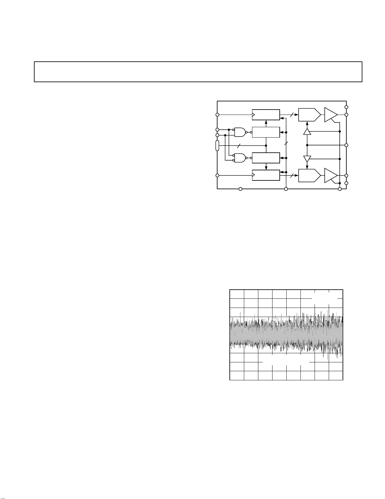
The AD7396/AD7397 series of dual, 12-bit and 10-bit voltageoutput digital-to-analog converters are designed to operate from
a single +3 V supply. Built using a CBCMOS process, these
monolithic DACs offer the user low cost and ease of use in
single supply +3 V systems. Operation is guaranteed over the
supply voltage range of +2.7 V to +5.5 V, making this device
ideal for battery operated applications.
A 12-bit wide data latch loads with a 45 ns write time allowing
interface to fast processors without wait states. The double
buffered input structure allows the user to load the input
registers one at a time, then a single load strobe tied to both
LDA+LDB inputs will simultaneously update both DAC outputs. LDA and LDB can also be independently activated to
immediately update their respective DAC registers. An address
input (A/B) decodes DACA or DACB when the chip select CS
input is strobed. Additionally, an asynchronous RS input sets
the output to zero-scale at power on or upon user demand.
Power shutdown to submicroamp levels is directly controlled by
the active low SHDN pin. While in the power shutdown state
register data can still be changed even though the output buffer
is in an open circuit state. Upon return to the normal operating
state the latest data loaded in the DAC register will establish the
output voltage.
Dual 12-Bit /10-Bit DACs
AD7396/AD7397
FUNCTIONAL BLOCK DIAGRAM
V
DD
V
OUTA
V
REF
V
OUTB
AGND
LDA
CS
A/B
DATA
LDB
AD7396
12
DGND
DACA
REGISTER
INPUTA
REGISTER
INPUTB
REGISTER
DACB
REGISTER
12
12-BIT
DACA
1
12
12-BIT
DACB
RS SHDN
Both parts are offered in the same pinout, allowing users to
select the amount of resolution appropriate for their applications
without circuit card changes.
The AD7396/AD7397 are specified for operation over the ex-
tended industrial (–40°C to +85°C) temperature range. The
AD7397AR is specified for the –40°C to +125°C automotive
temperature range. AD7396/AD7397s are available in plastic
DIP, and 24-lead SOIC packages. The AD7397ARU is available for ultracompact applications in a thin 1.1 mm height
TSSOP 24-lead package.
1.0
0.8
0.6
0.4
0.2
0.0
DNL – LSB
–0.2
–0.4
–0.6
–0.8
–1.0
0
TA = +258C, +858C, –558C
SUPERIMPOSED
512 1024 1536 2048 2560 3072 3584 4096
CODE – Decimal
VDD = +3V
= +2.5V
V
REF
Figure 1. DNL vs. Digital Code at Temperature
REV. 0
Information furnished by Analog Devices is believed to be accurate and
reliable. However, no responsibility is assumed by Analog Devices for its
use, nor for any infringements of patents or other rights of third parties
which may result from its use. No license is granted by implication or
otherwise under any patent or patent rights of Analog Devices.
One Technology Way, P.O. Box 9106, Norwood, MA 02062-9106, U.S.A.
Tel: 781/329-4700 World Wide Web Site: http://www.analog.com
Fax: 781/326-8703 © Analog Devices, Inc., 1998

AD7396/AD7397–SPECIFICATIONS
AD7396 12-BIT
ELECTRICAL CHARACTERISTICS
(@ V
= +2.5 V, –40ⴗC < TA < +85ⴗC, unless otherwise noted)
REF IN
Parameter Symbol Conditions +3 V ⴞ 10% +5 V ⴞ 10% Units
STATIC PERFORMANCE
Resolution
Relative Accuracy
Relative Accuracy
Differential Nonlinearity
Differential Nonlinearity
Zero-Scale Error V
Zero-Scale Error V
Full-Scale Voltage Error V
Full-Scale Voltage Error V
Full-Scale Tempco
1
2
2
2
2
3
N 12 12 Bits
INL T
INL T
DNL T
= +25°C ±1.75 ±1.75 LSB max
A
= –40°C, +85°C ±2.0 ±2.0 LSB max
A
= +25°C, Monotonic ±0.9 ±0.9 LSB max
A
DNL Monotonic ±1 ±1 LSB max
ZSE
ZSE
FSE
FSE
TCV
FS
Data = 000H, T
Data = 000H, T
T
= +25°C, +85°C, Data = FFFH±8 ±8mV max
A
T
= –40°C, Data = FFF
A
= +25°C, +85°C 4.0 4.0 mV max
A
= –40°C 8.0 8.0 mV max
A
H
±20 ±20 mV max
–45 –45 ppm/°C typ
REFERENCE INPUT
V
Range V
REF
Input Resistance R
Input Capacitance
3
REF
REF
C
REF
0/V
DD
0/V
DD
V min/max
2.5 2.5 MΩ typ
55pF typ
ANALOG OUTPUT
Output Current (Source) I
Output Current (Sink) I
Capacitive Load
3
OUT
OUT
C
L
Data = 800
Data = 800
H
H
, ∆V
, ∆V
= 5 LSB 1 1 mA typ
OUT
= 5 LSB 3 3 mA typ
OUT
No Oscillation 100 100 pF typ
LOGIC INPUTS
Logic Input Low Voltage V
Logic Input High Voltage V
Input Leakage Current I
Input Capacitance
INTERFACE TIMING
3
3, 5
Chip Select Write Width t
DAC Select Setup t
DAC Select Hold t
Data Setup t
Data Hold t
Load Setup t
Load Hold t
Load Pulsewidth t
Reset Pulsewidth t
IL
C
CS
AS
AH
DS
DH
LS
LH
LDW
RSW
IL
IH
IL
0.5 0.8 V max
VDD – 0.6 4.0 V min
10 10 µA max
10 10 pF max
45 35 ns min
30 15 ns min
0 0 ns min
30 15 ns min
20 10 ns min
20 20 ns min
10 10 ns min
30 30 ns min
40 30 ns min
AC CHARACTERISTICS
Output Slew Rate SR Data = 000
Settling Time
Shutdown Recovery Time t
6
t
S
SDR
To ±0.1% of Full Scale 70 60 µs typ
DAC Glitch Q Code 7FF
to FFFH to 000
H
to 800H to 7FF
H
H
0.05 0.05 V/µs typ
90 80 µs typ
H
65 65 nV/s typ
Digital Feedthrough Q 15 15 nV/s typ
V
Feedthrough V
OUT/VREF
= 1.5 VDC +1 V p-p
REF
,
Data = 000H, f = 100 kHz –63 –63 dB typ
SUPPLY CHARACTERISTICS
Power Supply Range V
Positive Supply Current I
Shutdown Supply Current I
Power Dissipation P
DD RANGE
DD
DD_SD
DISS
DNL < ±1 LSB 2.7/5.5 2.7/5.5 V min/max
V
= 0 V, No Load 125/200 125/200 µA typ/max
IL
SHDN = 0, V
V
= 0 V, No Load 600 1000 µW max
IL
= 0 V, No Load 0.1/1.5 0.1/1.5 µA typ/max
IL
Power Supply Sensitivity PSS ∆VDD = ±5% 0.006 0.006 %/% max
NOTES
1
One LSB = V
2
The first two codes (000H, 001H) are excluded from the linearity error measurement.
3
These parameters are guaranteed by design and not subject to production testing.
4
Typicals represent average readings measured at +25°C.
5
All input control signals are specified with tR = tF = 2 ns (10% to 90% of +3 V) and timed from a voltage level of +1.6 V.
6
The settling time specification does not apply for negative going transitions within the last 3 LSBs of ground.
Specifications subject to change without notice.
/4096 V for the 12-bit AD7396.
REF
–2–
4
REV. 0

AD7397 10-BIT
AD7396/AD7397
ELECTRICAL CHARACTERISTICS
(@ V
= +2.5 V, –40ⴗC < TA < +85ⴗC, unless otherwise noted)
REF IN
Parameter Symbol Conditions +3 V ⴞ 10% +5 V ⴞ 10% Units
STATIC PERFORMANCE
Resolution
Relative Accuracy
Relative Accuracy
Differential Nonlinearity
Zero-Scale Error V
Full-Scale Voltage Error V
Full-Scale Voltage Error V
Full-Scale Tempco
1
2
2
2
3
N 10 10 Bits
INL T
INL T
= +25°C ±1.75 ±1.75 LSB max
A
= –40°C, +85°C, +125°C ±2.0 ±2.0 LSB max
A
DNL Monotonic ±1 ±1LSB max
ZSE
FSE
FSE
TCV
FS
Data = 000
T
= +25°C, +85°C, +125°C, Data = 3FFH±42 ±42 mV max
A
T
= –40°C, Data = 3FF
A
H
H
9.0 9.0 mV max
±48 ±48 mV max
–45 –45 ppm/°C typ
REFERENCE INPUT
V
Range V
REF
Input Resistance R
Input Capacitance
3
REF
REF
C
REF
0/V
DD
0/V
DD
V min/max
2.5 2.5 MΩ typ
5 5 pF typ
ANALOG OUTPUT
Output Current (Source) I
Output Current (Sink) I
Capacitive Load
3
C
OUT
OUT
L
Data = 200
Data = 200
H
H
, ∆V
, ∆V
= 5 LSB 1 1 mA typ
OUT
= 5 LSB 3 3 mA typ
OUT
No Oscillation 100 100 pF typ
LOGIC INPUTS
Logic Input Low Voltage V
Logic Input High Voltage V
Input Leakage Current I
Input Capacitance
INTERFACE TIMING
3
3, 5
Chip Select Write Width t
DAC Select Setup t
DAC Select Hold t
Data Setup t
Data Hold t
Load Setup t
Load Hold t
Load Pulsewidth t
Reset Pulsewidth t
IL
C
CS
AS
AH
DS
DH
LS
LH
LDW
RSW
IL
IH
IL
0.5 0.8 V max
VDD – 0.6 4.0 V min
10 10 µA max
10 10 pF max
45 35 ns min
30 15 ns min
0 0 ns min
30 15 ns min
20 10 ns min
20 20 ns min
10 10 ns min
30 30 ns min
40 30 ns min
AC CHARACTERISTICS
Output Slew Rate SR Data = 000
Settling Time
Shutdown Recovery Time t
6
t
S
SDR
To ±0.1% of Full Scale 70 60 µs typ
DAC Glitch Q Code 7FF
to 3FFH to 000
H
to 800H to 7FF
H
H
0.05 0.05 V/µs typ
90 80 µs typ
H
65 65 nV/s typ
Digital Feedthrough Q 15 15 nV/s typ
Feedthrough V
OUT/VREFVREF
= 1.5 VDC +1 V p-p
,
Data = 000H, f = 100 kHz –63 –63 dB typ
SUPPLY CHARACTERISTICS
Power Supply Range V
Positive Supply Current I
Shutdown Supply Current I
Power Dissipation P
DD RANGE
DD
DD_SD
DISS
DNL < ±1 LSB 2.7/5.5 2.7/5.5 V min/max
V
= 0 V, No Load 125/200 125/200 µA typ/max
IL
SHDN = 0, V
V
= 0 V, No Load 600 1000 µW max
IL
= 0 V, No Load 0.1/1.5 0.1/1.5 µA typ/max
IL
Power Supply Sensitivity PSS ∆VDD = ±5% 0.006 0.006 %/% max
NOTES
1
One LSB = V
2
The first two codes (000H, 001H) are excluded from the linearity error measurement.
3
These parameters are guaranteed by design and not subject to production testing.
4
Typicals represent average readings measured at +25°C.
5
All input control signals are specified with tR = tF = 2 ns (10% to 90% of +3 V) and timed from a voltage level of +1.6 V.
6
The settling time specification does not apply for negative going transitions within the last 3 LSBs of ground.
Specifications subject to change without notice.
/4096 V for the 10-bit AD7397.
REF
4
–3–REV. 0

AD7396/AD7397
t
CS
A/B
D0–D11
LDA, LDB
RS
V
OUT
CSW
t
LS
t
AS
t
DS
t
AH
t
DH
t
t
RSW
t
S
LDW
1 LSB
ERROR BAND
t
LH
t
S
DBx
CS
A/B
RS
B REGISTER
1 OF 12
LATCHES
OF THE 2 INPUT
REGISTERS
TO DAC
REGISTERS
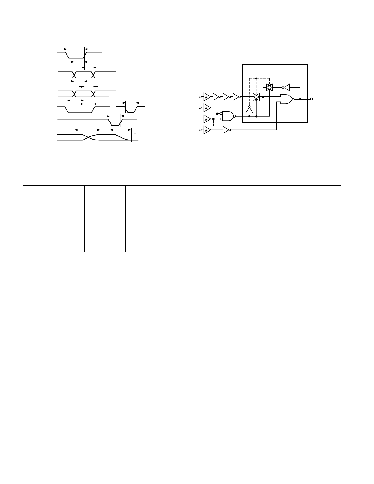
Figure 2. Timing Diagram
Figure 3. Digital Control Logic
Table I. Control Logic Truth
CS A/B LDA LDB RS SHDN Input Register DAC Register
L L HHHX Write to B Latched with Previous Data
L HHHHX Write to A Latched with Previous Data
L L H L H X Write to B B Transparent
L H L H H X Write to A A Transparent
H X L L H X Latched A and B Transparent
H X ^ ^ H X Latched Latched with New Data from Input REG
XXXXLX Reset to Zero Scale Reset to Zero Scale
HXXX^ X Latched to Zero Latched to Zero
^Denotes positive edge. The SHDN pin has no effect on the digital interface data loading; however, while in the SHDN state (SHDN = 0) the output amplifiers V
and V
exhibit an open circuit condition. Note, the LDx inputs are level-sensitive, the respective DAC registers are in a transparent state when LDx = “0.”
OUTB
OUTA
–4–
REV. 0
 Loading...