Analog Devices AD7112 Datasheet

LC2MOS LOGDAC
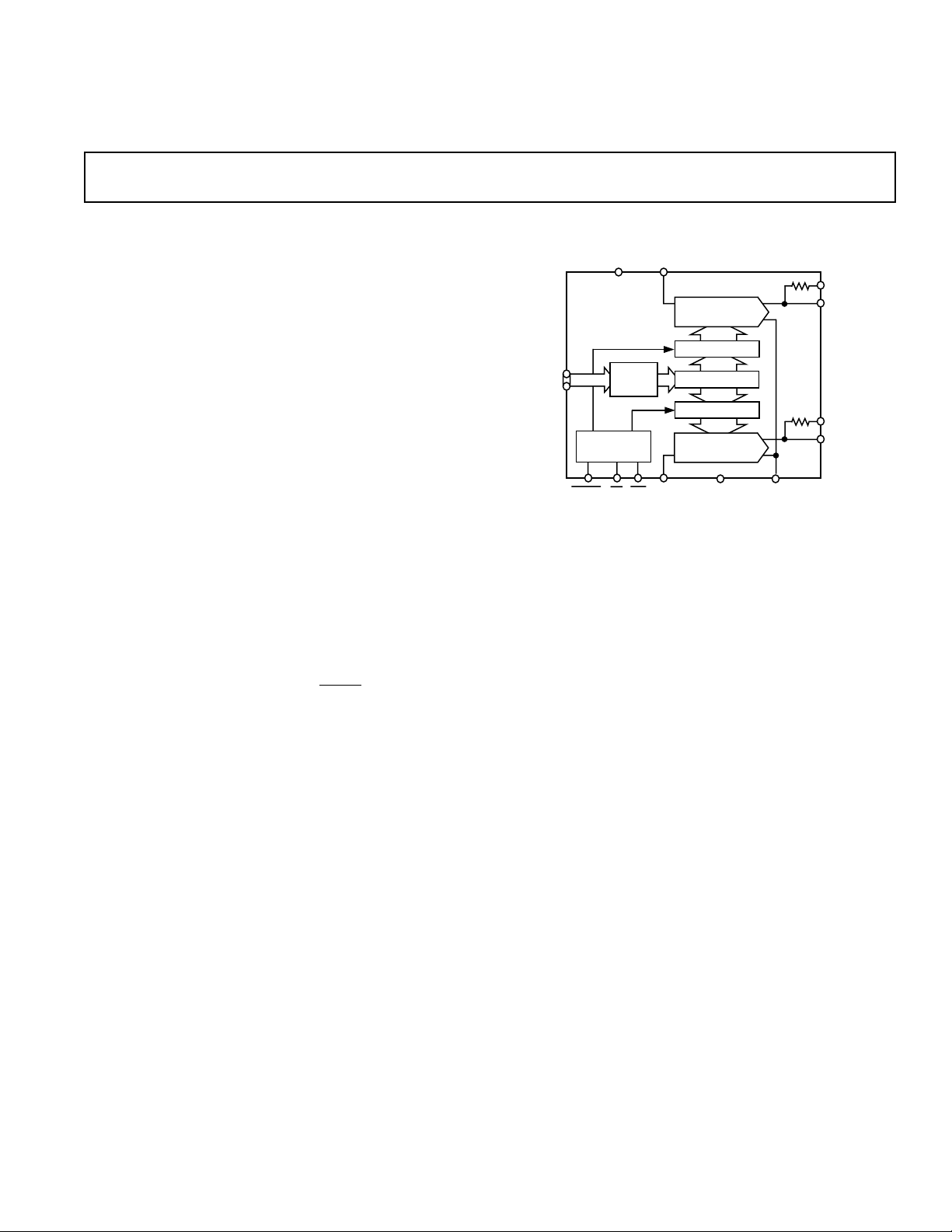
17-BIT DAC A
AD7112
OUT A
AGND
DGND
CS
WR
17-BIT LATCH
17
17-BIT LATCH
17-BIT DAC B
R
FB
A
OUT B
RFB B
DECODE LOGIC
VIN B
V
IN
A
DAC A/
DAC B
CONTROL
LOGIC
8-BIT
BUFFER
DB0
DB7
V
DD
a
FEATURES
Dynamic Range: 88.5 dB
Resolution: 0.375 dB
On-Chip Data Latches for Both DACs
Four-Quadrant Multiplication
+5 V Operation
Pin Compatible with AD7528
Low Power
APPLICATIONS
Audio Attenuators
Sonar Systems
Function Generators
GENERAL DESCRIPTION
The LOGDAC® AD7112 is a monolithic dual multiplying D/A
converter featuring wide dynamic range and excellent DAC-toDAC matching. Both DACs can attenuate an analog input signal over the range 0 dB to 88.5 dB in 0.375 dB steps. It is
available in skinny 0.3" wide 20-pin DIPs and in 20-terminal
surface mount packages.
The degree of attenuation in either channel is determined by the
8-bit word applied to the onboard decode logic. This 8-bit word
is decoded into a 17-bit word which is then loaded into one of
the 17-bit data latches, determined by
step resolution over the entire dynamic range is due to the use of
these 17-bit DACs.
The AD7112 is easily interfaced to a standard 8-bit MPU bus
via an 8-bit data port and standard microprocessor control lines.
It should be noted that the AD7112 is exactly pin-compatible
with the AD7528, an industry standard dual 8-bit multiplying
DAC. This allows an easy upgrading of existing AD7528 designs which would benefit both from the wider dynamic range
and the finer step resolution offered by the AD7112.
The AD7112 is fabricated in Linear Compatible CMOS
2
(LC
MOS), an advanced, mixed technology process that com-
bines precision bipolar circuits with low power CMOS logic.
DACA/DACB. The fine
Dual Logarithmic D/A Converter
AD7112*
FUNCTIONAL BLOCK DIAGRAM
PRODUCT HIGHLIGHTS
1. DAC-to-DAC Matching: Since both of the AD7112 DACs
are fabricated at the same time on the same chip, precise
matching and tracking between the two DACs is inherent.
2. Small Package: The AD7112 is available in a 20-pin DIP
and a 20-terminal SOIC package.
3. Fast Microprocessor Interface: The AD7112 has bus interface timing compatible with all modern microprocessors.
*Protected by U.S. Patent No. 4521764.
LOGDAC is a registered trademark of Analog Devices, Inc.
REV. 0
Information furnished by Analog Devices is believed to be accurate and
reliable. However, no responsibility is assumed by Analog Devices for its
use, nor for any infringements of patents or other rights of third parties
which may result from its use. No license is granted by implication or
otherwise under any patent or patent rights of Analog Devices.
One Technology Way, P.O. Box 9106, Norwood, MA 02062-9106, U.S.A.
Tel: 617/329-4700 Fax: 617/326-8703

AD7112–SPECIFICA TIONS
Output amplifier AD712 except where noted. All specifications T
C Version
T
=T
Parameter +258CT
A
A
MIN
(VDD = +5 V 6 5%; OUT A = OUT B = AGND = DGND = 0 V; VIN A = VIN B = 10 V.
to T
MIN
1
=T
, T
MAX
+258CT
unless otherwise noted.)
MAX
B Version
=T
A
=
A
, T
MIN
Units Conditions/Comments
MAX
ACCURACY
Resolution 0.375 0.375 0.375 0.375 dB
Accuracy Relative to Guaranteed Attenuation
0 dB Attenuation Ranges for Specified Step Sizes.
0.375 dB Steps:
Accuracy ≤ ±0.17 dB 0 to 36 0 to 36 0 to 30 0 to 30 dB min
Monotonic 0 to 54 0 to 54 0 to 48 0 to 48 dB min
0.75 dB Steps:
Accuracy ≤ ±0.35 dB 0 to 48 0 to 42 0 to 42 0 to 36 dB min
Monotonic 0 to 72 0 to 66 0 to 72 0 to 60 dB min
1.5 dB Steps:
Accuracy ≤ ±0.7 dB 0 to 54 0 to 48 0 to 48 0 to 42 dB min
Monotonic Full Range 0 to 78 0 to 85.5 0 to 72 dB min Full Range Is 0 dB to 88.5 dB.
3.0 dB Steps:
Accuracy ≤ ±1.4 dB 0 to 66 0 to 54 0 to 60 0 to 48 dB min
Monotonic Full Range Full Range Full Range Full Range dB min
6.0 dB Steps:
Accuracy ≤ ±2.7 dB 0 to 72 0 to 60 0 to 60 0 to 60 dB min
Monotonic Full Range Full Range Full Range Full Range dB min
Gain Error ±0.1 ±0.15 ±0.15 ±0.2 dB max Measured Using R
R
B. Both DAC Registers
FB
FB
A,
Loaded With All 0s.
Output Leakage Current
OUT A, OUT B ±50 ±400 ±50 ±400 nA max
Input Resistance,
V
A, VIN B 9/15 9/15 9/15 9/15 kΩ min/max Typically 12 kΩ.
IN
Input Resistance Match ±1 ±1 ±2 ±2 % max
Feedback Resistance,
RFB A, RFB B 9.3/15.7 9.3/15.7 9.3/15.7 9.3/15.7 kΩ min/max
LOGIC INPUTS
CS, WR,
DAC A/DAC B,
DB0–DB7
Input Low Voltage, V
Input High Voltage, V
Input Leakage Current ±1 ± 10 ±1 ± 10 µA max
Input Capacitance
POWER REQUIREMENTS
V
DD
, Range
3
2
0.8 0.8 0.8 0.8 V max
INL
2.4 2.4 2.4 2.4 V min
INH
10 10 10 10 pF max
4.75/5.25 4.75/5.25 4.75/5.25 4.75/5.25 V min/max For Specified Performance.
2 2 2 2 mA max Logic Inputs = V
2 2 2 2 mA max Logic Inputs = 0 V or V
NOTES
l
Temperature range as follows: B, C Versions: –40°C to +85 °C.
2
Guaranteed by design, not production tested.
3
The part will function with VDD = 5 V ± 10% with degraded performance.
Specifications subject to change without notice.
or V
IL
IH
DD
–2–
REV. 0

AD7112
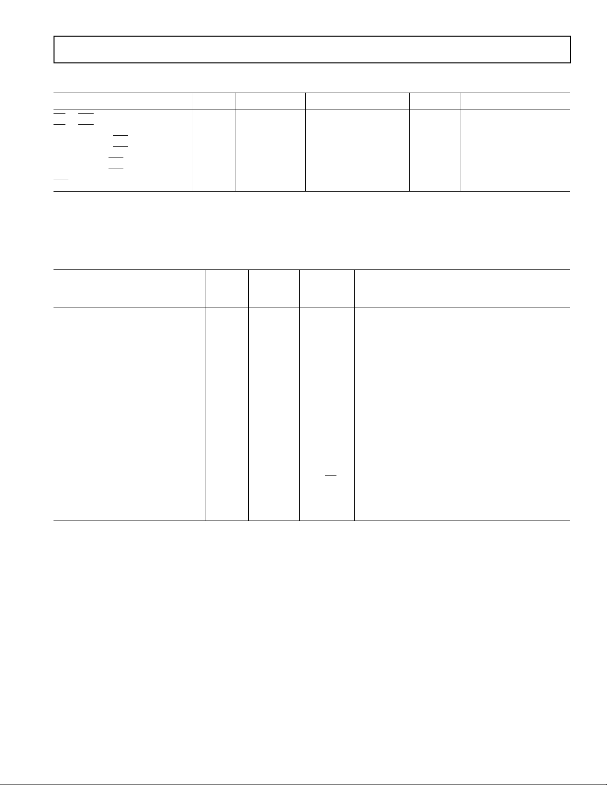
TIMING SPECIFICATIONS
Parameter TA = +258CT
CS to WR Setup Time t
CS to WR Hold Time t
DAC Select to
DAC Select to
Data Valid to
Data Valid to
WR Setup Time t
WR Hold Time t
WR Setup Time t
WR Hold Time t
WR Pulse Width t
NOTES
1
Timing specifications guaranteed by design not production tested. All input signals are specified with tr = tf = 5 ns (10% to 90% of 5 V) and timed from a voltage
level of 1.6 V.
Specifications subject to change without notice.
AC PERFORMANCE CHARACTERISTICS
1
(VDD = +5 V 6 5%; 0UT A = OUT B = AGND = DGND = O V; VIN A = VIN B = 10 V)
= –408C to +858C Units Conditions/Comments
A
CS
CH
AS
AH
DS
DH
WR
0 0 ns min See Figure 3.
0 0 ns min
4 4 ns min
0 0 ns min
55 55 ns min
10 10 ns min
53 53 ns min
(VDD = +5 V 6 5%; 0UT A = OUT B = AGND = DGND = 0 V; VIN A =
1
VIN B = 10 V. Output amplifier AD712 except where noted.)
TA =
T
= –408C to
A
Parameter +258C +858C Units Conditions/Comments
DC Supply Rejection ∆ Gain/∆ V
0.001 0.005 dB/% max ∆ VDD = ± 5%. Input Code = 00000000
DD
Digital-to-Analog Glitch Impulse 10 10 nV s typ Measured with AD843 as output amplifier for input
code transition 10000000 to 00000000.
Output Capacitance, C
OUT A
, C
OUT B
50 50 pF max
AC Feedthrough
V
A to OUT A –94 –90 dB max VIN A, VIN B = 6 V rms at 1 kHz. DAC
IN
Registers loaded with all 1s.
V
B to OUT B –94 –90 dB max
IN
Channel-to-Channel Isolation
V
A to OUT B –87 –87 dB typ VIN A = 6 V rms at 10 kHz sine wave,
IN
V
B to OUT A –87 –87 dB typ VIN B = 6 V rms at 10 kHz sine wave,
IN
V
B = 0 V. DAC Registers loaded with all 0s.
IN
V
A = 0 V. DAC Registers loaded with all 0s.
IN
Digital Feedthrough 1 1 nV s typ Measured with input code transitions of all 0s to all 1s.
Output Noise Voltage Density
(30 Hz to 50 kHz) 15 15 nV/√
Total Harmonic Distortion –91 –91 dB typ V
Hz typ Measured between RFB A and OUT A or between
R
B and OUT B.
FB
A = VIN B = 6 V rms at 1 kHz. DAC
IN
Registers loaded with all 0s.
NOTES
1
Guaranteed by design, not production tested.
Specifications subject to change without notice.
REV. 0
–3–

AD7112
WARNING!
ESD SENSITIVE DEVICE
ABSOLUTE MAXIMUM RATINGS*
VDD to AGND or DGND . . . . . . . . . . . . . . . . . .–0.3 V, +7 V
AGND to DGND . . . . . . . . . . . . . . . . . . –0.3 V, V
Digital Inputs to DGND . . . . . . . . . . . . . –0.3 V, V
OUT A, OUT B to AGND . . . . . . . . . . . –0.3 V, V
V
A, VIN B to AGND . . . . . . . . . . . . . . . . . . . . . . . . . ±25 V
IN
V
RFB
A, V
B to AGND . . . . . . . . . . . . . . . . . . . . . . . ±25 V
RFB
+ 0.3 V
DD
+ 0.3 V
DD
+ 0.3 V
DD
Operating Temperature Range
All Versions . . . . . . . . . . . . . . . . . . . . . . . . –40°C to +85°C
Junction Temperature . . . . . . . . . . . . . . . . . . . . . . . . +150°C
Storage Temperature . . . . . . . . . . . . . . . . . –65°C to +150°C
Power Dissipation, DIP . . . . . . . . . . . . . . . . . . . . . . . . . . 1 W
θ
, Thermal Impedance . . . . . . . . . . . . . . . . . . . . . 102°C/W
JA
Lead Temperature (Soldering, 10 secs) . . . . . . . . . . . +300°C
Power Dissipation, SOIC . . . . . . . . . . . . . . . . . . . . . . . . . 1 W
θ
, Thermal Impedance . . . . . . . . . . . . . . . . . . . . . . 75°C/W
JA
Lead Temperature (Soldering)
Vapor Phase (60 secs) . . . . . . . . . . . . . . . . . . . . . . . .215°C
Infrared (15 secs) . . . . . . . . . . . . . . . . . . . . . . . . . . . .220°C
*Stresses above those listed under “Absolute Maximum Ratings” may cause
permanent damage to the device. This is a stress rating only and functional
operation of the device at these or any other conditions above those listed in the
operational sections of this specification is not implied. Exposure to absolute
maximum rating conditions for extended periods may affect device reliability. Only
one Absolute Maximum Rating may be applied at any one time.
CAUTION
ESD (electrostatic discharge) sensitive device. Electrostatic charges as high as 4000 V readily
accumulate on the human body and test equipment and can discharge without detection.
Although the AD7112 features proprietary ESD protection circuitry, permanent damage may
occur on devices subjected to high energy electrostatic discharges. Therefore, proper ESD
precautions are recommended to avoid performance degradation or loss of functionality.
TERMINOLOGY
PIN FUNCTION DESCRIPTION
RESOLUTION: Nominal change in attenuation when moving
between two adjacent codes.
MONOTONICITY: The device is monotonic if the analog output decreases or remains constant as the wdigital code increases.
FEEDTHROUGH ERROR: That portion of the input signal
which reaches the output when all digital inputs are high.
OUTPUT CAPACITANCE: Capacitance from OUT A or
OUT B to ground.
GAIN ERROR: Gain error results from a mismatch between
R
(the feedback resistance) and the R-2R ladder resistance.
FB
Its effect in a LOGDAC is to produce a constant additive attenuation error in dB over the whole range of the DAC.
ACCURACY: The difference (measured in dB) between the
ideal transfer function as listed in Table I and the actual transfer function as measured with the device.
DIGITAL-TO-ANALOG GLITCH IMPULSE: The amount
Pin Mnemonic Description
1 AGND Analog Ground.
2 OUT A Current Output Terminal of DAC A.
3R
4V
A Feedback Resistor for DAC A.
FB
A Reference Input to DAC A
IN
5 DGND Digital Ground.
6
DAC A/ Selects Which DAC Can Accept Data from
DAC B Input Port.
7–14 DB7–DB0 8 Data Inputs.
15
CS Chip Select Input, Active Low.
16
WR Write Input, Active Low.
17 V
18 V
19 R
DD
B Reference Input to DAC B.
IN
B Feedback Resistor for DAC B.
FB
Power Supply Input 5 V ± 5%.
20 OUT B Current Output Terminal of DAC B.
of charge injected from the digital inputs to the analog output
when the inputs change state. This is normally specified as the
area of the glitch in either pA-s or nV-s depending on whether
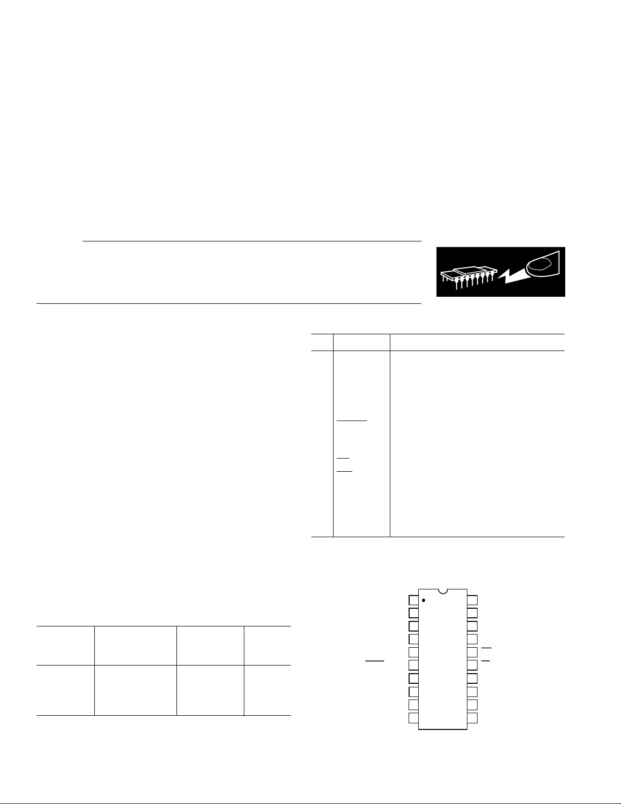
PIN CONFIGURATION
DIP/SOIC
the glitch is measured as a current or voltage signal. Glitch impulse is measured with V
ORDERING INFORMATION
Temperature Accuracy Package
Model Range Range Option*
AD7112BN –40°C to +85°C 0 dB to 60 dB N-20
AD7112CN –40°C to +85°C 0 dB to 72 dB N-20
AD7112BR –40°C to +85°C 0 dB to 60 dB R-20
AD7112CR –40°C to +85°C 0 dB to 72 dB R-20
*N = Plastic DIP; R = SOIC.
= AGND.
IN
Specified
AGND
OUT A
R
FB
V
IN
DGND
DAC A/DAC B
(MSB) DB7
DB6
DB5
DB4
A
A
1
2
3
4
5
6
(Not to Scale)
7
8
9
10
AD7112
TOP VIEW
20
19
18
17
16
15
14
13
12
11
OUT B
R
B
FB
V
B
IN
V
DD
WR
CS
DB0 (LSB)
DB1
DB2
DB3
–4–
REV. 0
 Loading...