

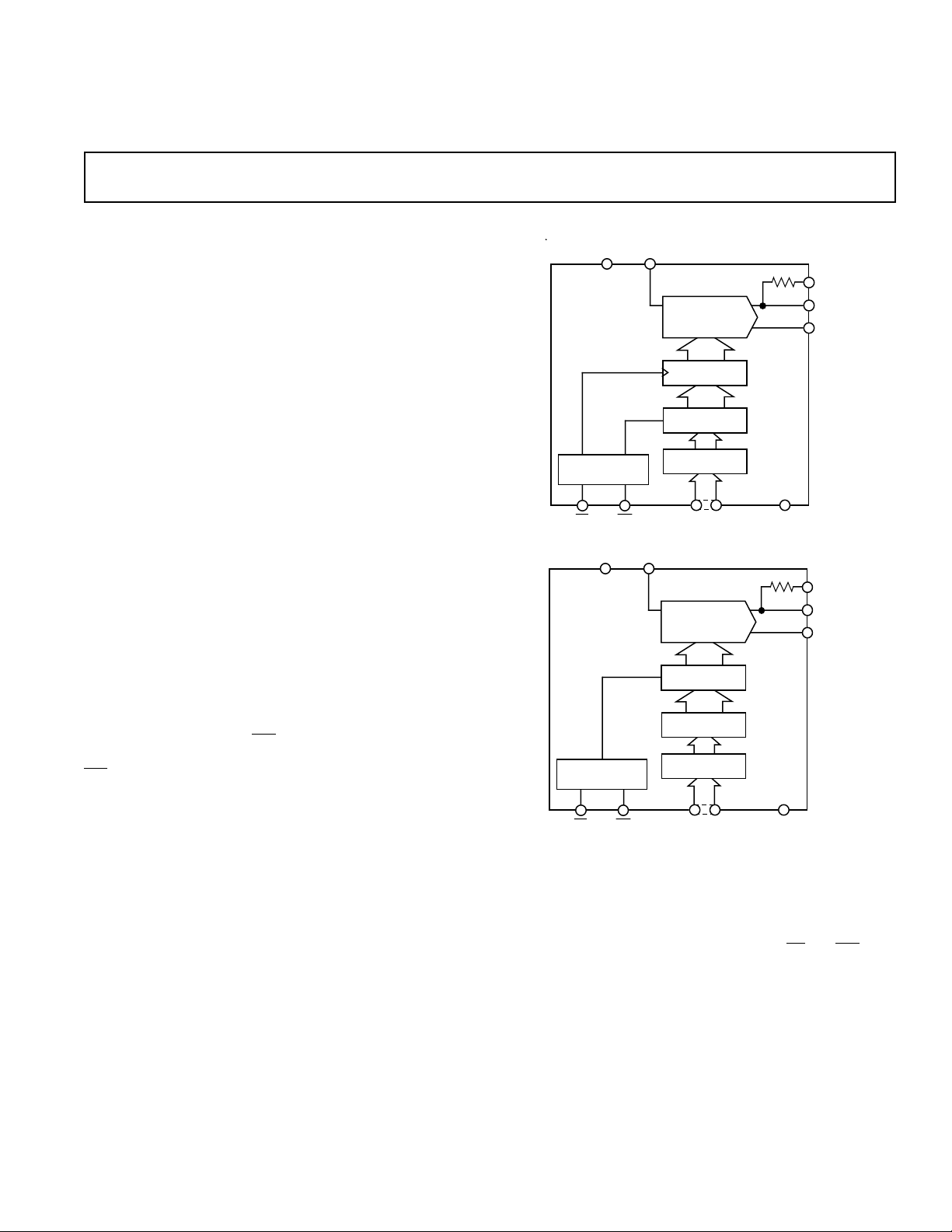
LC2MOS LOGDAC
17-BIT DAC
17-BIT LATCH
DECODE LOGIC
8-BIT BUFFER
CONTROL LOGIC
AD7111A
I
OUT
AGND
R
FB
V
DD
V
IN
DGND
CS
WR
D0 – D7
a
FEATURES
Dynamic Range: 88.5 dB
Resolution: 0.375 dB
On-Chip Data Latches
+5 V Operation
AD7111A Pin Compatible with AD7524
Low Power
APPLICATIONS
Audio Attenuators
Sonar Systems
Function Generators
Digitally Controlled AGC System
GENERAL DESCRIPTION
The LOGDAC AD7111/AD7111A are monolithic multiplying
D/A converters featuring wide dynamic range in a small package. Both DACs can attenuate an analog input signal over the
range 0 dB to 88.5 dB in 0.375 dB steps. They are available in
16-pin DIPs and SOIC packages. The AD7111 is also available
in a 20-terminal LCCC package.
The degree of attenuation across the DAC is determined by an
8-bit word applied to the onboard decode logic. This 8-bit word
is decoded into a 17-bit word which is then applied to a 17-bit
R-2R ladder. The very fine step resolution, which is available
over the entire dynamic range, is due to the use of this 17-bit
DAC.
The AD7111/AD7111A are easily interfaced to a standard 8-bit
MPU bus via an 8-bit data port and standard microprocessor
control lines. The AD7111
quires a rising edge to load new data to the DAC. The AD7111A
WR is level triggered to allow transparent operation of the
latches, if required. It should also be noted that the AD7111A is
exactly pin and function-compatible with the AD7524, an industry standard 8-bit multiplying DAC. This allows an easy upgrading of existing AD7524 designs which would benefit both
from the wider dynamic range and the finer step resolution offered by the AD7111A.
The AD7111/AD7111A are fabricated in Linear Compatible
CMOS (LC2MOS), an advanced, mixed technology process that
combines precision bipolar circuits with low power CMOS logic.
LOGDAC is a registered trademark of Analog Devices, Inc.
WR input is edge triggered and re-
Logarithmic D/A Converter
AD7111/AD7111A
FUNCTIONAL BLOCK DIAGRAMS
V
V
DD
IN
R
FB
AD7111
17-BIT DAC
17-BIT LATCH
DECODE LOGIC
CONTROL LOGIC
WR
CS
8-BIT BUFFER
D0 – D7
DGND
PRODUCT HIGHLIGHTS
1. Wide Dynamic Range: 0 dB to 88.5 dB attenuation range in
0.375 dB steps.
2. Small Package: The AD7111/AD7111A are available in
16-pin DIPs and SOIC packages.
3. Transparent Latch Operation: By tying the
puts low, the DAC latches in the AD7111A can be made
transparent.
4. Fast Microprocessor Interface: Data setup times of 25 ns and
write pulse width of 57 ns make the AD7111A compatible
with modern microprocessors.
I
OUT
AGND
CS and WR in-
REV. 0
Information furnished by Analog Devices is believed to be accurate and
reliable. However, no responsibility is assumed by Analog Devices for its
use, nor for any infringements of patents or other rights of third parties
which may result from its use. No license is granted by implication or
otherwise under any patent or patent rights of Analog Devices.
One Technology Way, P.O. Box 9106, Norwood, MA 02062-9106, U.S.A.
Tel: 617/329-4700 Fax: 617/326-8703
AD7111/AD7111A–SPECIFICA TIONS
(VDD = +5 V, VIN = –10 V dc, I
AD7111–ELECTRICAL CHARACTERISTICS
AD711 except where noted)
= AGND = DGND = O V output amplifier
OUT
Parameter TA = +258CTA = T
NOMINAL RESOLUTION 0.375 0.375 0.375 0.375 dB
ACCURACY RELATIVE TO
0 dB ATTENUATION
0.375 dB Steps:
Accuracy ≤ ±0.17 dB 0 to 36 0 to 36 0 to 30 0 to 30 dB min Guaranteed Attenuation Ranges
Monotonic 0 to 54 0 to 54 0 to 48 0 to 48 dB min for Specified Step Sizes
0.75 dB Steps:
Accuracy ≤ ±0.35 dB 0 to 48 0 to 42 0 to 42 0 to 36 dB min
Monotonic 0 to 72 0 to 66 0 to 72 0 to 60 dB min
1.5 dB Steps:
Accuracy ≤ ±0.7 dB 0 to 54 0 to 48 0 to 42 0 to 42 dB min Full Range Is from 0 dB
Monotonic Full Range 0 to 78 0 to 85.5 0 to 72 dB min to 88.5 dB
3.0 dB Steps:
Accuracy ≤ ±1.4 dB 0 to 66 0 to 54 0 to 60 0 to 48 dB min
Monotonic Full Range Full Range Full Range Full Range dB min
6.0 dB Steps:
Accuracy ≤ ±2.7 dB 0 to 72 0 to 60 0 to 60 0 to 48 dB min
Monotonic Full Range Full Range Full Range Full Range dB min
GAIN ERROR ± 0.1 ± 0.15 ± 0.15 ±0.20 dB max
VIN INPUT RESISTANCE 9/11/15 9/11/15 7/11/18 7/11/18 kΩ min/typ/max
RFB INPUT RESISTANCE 9.3/11.5/15.7 9.3/11.5/15.7 7.3/11.5/18.8 7.3/11.5/18.8 kΩ min/typ/max
DIGITAL INPUTS
VIH (Input High Voltage) 2.4 2.4 2.4 2.4 V min
VIL (Input Low Voltage) 0.8 0.8 0.8 0.8 V max
Input Leakage Current ± 1 ±10 ± 1 ± 10 µA max Digital Inputs = V
SWITCHING CHARACTERISTICS
t
CS
t
CH
t
WR
t
DS
t
DH
t
RFSH
POWER SUPPLY
V
DD
I
DD
NOTE
1
Sample tested at +25°C to ensure compliance.
Specifications subject to change without notice.
AD7111L/C/U Grades AD7111K/B/T Grades
1
0 0 0 0 ns min
0 0 0 0 ns min Chip Select to Write Hold Time
350 500 350 500 ns min Write Pulse Width
175 250 175 250 ns min Data Valid to Write Setup Time
10 10 10 10 ns min Data Valid to Write Hold Time
3 4.5 3 4.5 µs min Refresh Time
+5 +5 +5 +5 V
1 4 1 4 mA max Digital Inputs = VIL or V
500 1000 500 1000 µA max Digital Inputs = 0 V or VDD;
MIN
, T
MAXTA
= +258CTA = T
MIN
, T
Units Conditions/Comments
MAX
Chip Select to Write Setup Time
See Figure 6
DD
IH
AC PERFORMANCE CHARACTERISTICS
to test. VDD = +5 V, VIN = –10 V dc except where noted, I
Parameter TA = +258CTA = T
DC Supply Rejection, ∆Gain/∆V
Propagation Delay 3.0 4.5 3.0 4.5 µs max Full-Scale Change Measured from
Digital-to-Analog Glitch Impulse 100 100 nV secs typ Measured with AD843 as Output
Output Capacitance, Pin 1 185 185 185 185 pF max
Input Capacitance, Pin 15 and Pin 16 7 7 7 7 pF max
Feedthrough at 1 kHz –94 –72 –94 –68 dB max
Total Harmonic Distortion –91 –91 –91 –91 dB typ VIN = 6 V rms at 1 kHz
Output Noise Voltage Density 70 70 70 70 nV/√Hz max Includes AD711 Amplifier Noise
Digital Input Capacitance 7 7 7 7 pF max
Specifications subject to change without notice.
DD
AD7111L/C/U Grades AD7111K/B/T Grades
0.001 0.005 0.001 0.005 dB per % max
These characteristics are included for design guidance only and are not subject
= AGND = DGND = O V, output amplifier AD711 except where noted.
OUT
MIN
, T
MAXTA
= +258CTA = T
MIN
, T
Units Conditions/Comments
MAX
∆VDD = ±10%, Input Code = 00000000
WR Going High, CS = 0 V
Amplifier for Code Transition
10000000 to 00000000
C1 of Figure 1 is 0 pF
–2–
REV. 0
AD7111/AD7111A
AD7111A–ELECTRICAL CHARACTERISTICS
(VDD = +5 V, VIN = –10 V dc, I
AD711 except where noted)
= AGND = DGND = O V output amplifier
OUT
AD7111AC Grade AD7111AB Grade
Parameter TA = +258CTA = T
MIN
, T
MAXTA
= +258CTA = T
MIN
, T
Units Conditions/Comments
MAX
NOMINAL RESOLUTION 0.375 0.375 0.375 0.375 dB
ACCURACY RELATIVE TO
0 dB ATTENUATION
0.375 dB Steps:
Accuracy ≤ ±0.17 dB 0 to 36 0 to 36 0 to 30 0 to 30 dB min Guaranteed Attenuation Ranges
Monotonic 0 to 54 0 to 54 0 to 48 0 to 48 dB min for Specified Step Sizes
0.75 dB Steps:
Accuracy ≤ ±0.35 dB 0 to 48 0 to 42 0 to 42 0 to 36 dB min
Monotonic 0 to 72 0 to 66 0 to 72 0 to 60 dB min
1.5 dB Steps:
Accuracy ≤ ±0.7 dB 0 to 54 0 to 48 0 to 48 0 to 42 dB min Full Range Is from 0 dB
Monotonic Full Range 0 to 78 0 to 85.5 0 to 72 dB min to 88.5 dB
3.0 dB Steps:
Accuracy ≤ ±1.4 dB 0 to 66 0 to 54 0 to 60 0 to 48 dB min
Monotonic Full Range Full Range Full Range Full Range dB min
6.0 dB Steps:
Accuracy ≤ ±2.7 dB 0 to 72 0 to 60 0 to 60 0 to 48 dB min
Monotonic Full Range Full Range Full Range Full Range dB min
GAIN ERROR ±0.1 ±0.15 ±0.15 ±0.20 dB max
VIN INPUT RESISTANCE 9/11/15 9/11/15 7/11/18 7/11/18 kΩ min/typ/max
RFB INPUT RESISTANCE 9.3/11.5/15.7 9.3/11.5/15.7 7.3/11.5/18.8 7.3/11.5/18.8 kΩ min/typ/max
DIGITAL INPUTS
VIH (Input High Voltage) 2.4 2.4 2.4 2.4 V min
VIL (Input High Voltage) 0.8 0.8 0.8 0.8 V max
Input Leakage Current ±1 ±10 ±1 ±10 µA max Digital Inputs = V
SWITCHING CHARACTERISTICS
t
CS
t
CH
t
WR
t
DS
t
DH
1
0 0 0 0 ns min
Chip Select to Write Setup Time
0 0 0 0 ns min Chip Select to Write Hold Time
57 57 57 57 ns min Write Pulse Width
25 25 25 25 ns min Data Valid to Write Setup Time
10 10 10 10 ns min Data Valid to Write Hold Time
POWER SUPPLY
V
DD
I
DD
+5 +5 +5 +5 V Digital Inputs = VIL or V
1 2 1 2 mA max CS = WR = 0 V
1 1 1 1 mA max Digital Inputs = 0 V or VDD;
See Figure 6
NOTE
1
Sample tested at +25°C to ensure compliance.
Specifications subject to change without notice.
DD
IH
AC PERFORMANCE CHARACTERISTICS
to test. VDD = +5 V, VIN = –10 V dc except where noted, I
These characteristics are included for design guidance only and are not subject
= AGND = DGND = O V, output amplifier AD711 except where noted.
OUT
AD7111AC Grade AD7111AB Grade
Parameter TA = +258CTA = T
DC Supply Rejection, ∆Gain/∆V
Propagation Delay 1 1.5 1 1.5 µs max Full-Scale Change Measured from
DD
0.001 0.005 0.001 0.005 dB per % max
MIN
, T
MAXTA
= +258CTA = T
MIN
, T
Units Conditions/Comments
MAX
∆VDD = ±10%, Input Code = 00000000
WR Going High, CS = 0 V
Digital-to-Analog Glitch Impulse 10 20 10 20 nV secs typ Measured with AD843 as Output
Amplifier for Code Transition
10000000 to 00000000
C1 of Figure 1 is 0 pF
Output Capacitance, Pin 1 50 50 50 50 pF max
Input Capacitance, Pin 15 and Pin 16 7 7 7 7 pF max
Feedthrough at 1 kHz –94 –90 –92 –90 dB max
Total Harmonic Distortion –91 –91 –91 –91 dB typ VIN = 6 V rms at 1 kHz
Output Noise Voltage Density 70 70 70 70 nV/√Hz max Includes AD711 Amplifier Noise
Digital Input Capacitance 7 7 7 7 pF max
Specifications subject to change without notice.
REV. 0
–3–

AD7111/AD7111A
WARNING!
ESD SENSITIVE DEVICE
ABSOLUTE MAXIMUM RATINGS*
(TA = +25°C unless otherwise noted)
VDD (to DGND) . . . . . . . . . . . . . . . . . . . . . . . . . . . . . . . +7 V
V
(to AGND) . . . . . . . . . . . . . . . . . . . . . . . . . . . . . . .±35 V
IN
Digital Input Voltage to DGND . . . . . –0.3 V to V
I
to AGND . . . . . . . . . . . . . . . . . . . . . . . . . .–0.3 V to V
OUT
V
to AGND . . . . . . . . . . . . . . . . . . . . . . . . . . . . . . .±35 V
RFB
AGND to DGND . . . . . . . . . . . . . . . . . . . . . . . . . . . 0 to V
DGND to AGND . . . . . . . . . . . . . . . . . . . . . . . . . . . 0 to V
+ 0.3 V
DD
DD
DD
DD
Power Dissipation, DIP . . . . . . . . . . . . . . . . . . . . . . . . . . 1 W
θ
, Thermal Impedance . . . . . . . . . . . . . . . . . . . . 117°C/W
JA
Lead Temperature (Soldering, 10 secs) . . . . . . . . . +300°C
Power Dissipation, SOIC . . . . . . . . . . . . . . . . . . . . . . . . . 1 W
θ
, Thermal Impedance . . . . . . . . . . . . . . . . . . . . . 75°C/W
JA
Power Dissipation, LCCC . . . . . . . . . . . . . . . . . . . . . . . . 1 W
θ
, Thermal Impedance . . . . . . . . . . . . . . . . . . . . . 76°C/W
JA
Lead Temperature (Soldering, 10 secs) . . . . . . . . . +300°C
Operating Temperature Range
Commercial (K, L Versions) . . . . . . . . . . . . .0°C to +70°C
Industrial (B, C Versions) . . . . . . . . . . . . . –40°C to +85°C
Extended (T, U Versions) . . . . . . . . . . . . –55°C to +125°C
Storage Temperature Range . . . . . . . . . . . . –65°C to +150°C
*Stresses above those listed under “Absolute Maximum Ratings” may cause
permanent damage to the device. This is a stress rating only, and functional
operation of the device at these or any other conditions above those listed in the
operational sections of this specification is not implied. Exposure to absolute
maximum rating conditions for extended periods may affect device reliability.
Lead Temperature (Soldering)
Vapor Phase (60 secs) . . . . . . . . . . . . . . . . . . . . . . .215°C
Infrared (15 secs) . . . . . . . . . . . . . . . . . . . . . . . . . .220°C
CAUTION
ESD (electrostatic discharge) sensitive device. Electrostatic charges as high as 4000 V readily
accumulate on the human body and test equipment and can discharge without detection.
Although the AD7111/AD7111A features proprietary ESD protection circuitry, permanent
damage may occur on devices subjected to high energy electrostatic discharges. Therefore,
proper ESD precautions are recommended to avoid performance degradation or loss of
functionality.
ORDERING GUIDES
AD7111A ORDERING GUIDE
Specified
Temperature Accuracy Package
Model Range Range Option
1
AD7111ABN –40°C to +85°C 0 dB to 60 dB N-16
AD7111ACN –40°C to +85°C 0 dB to 72 dB N-16
AD7111ABR –40°C to +85°C 0 dB to 60 dB R-16
AD7111ACR –40°C to +85°C 0 dB to 72 dB R-16
NOTE
1
N = Plastic DIP; R = SOIC.
TERMINOLOGY
RESOLUTION: Nominal change in attenuation when moving
between two adjacent codes. MONOTONICITY: The device is monotonic if the analog out-
put decreases (or remains constant) as the digital code increases. FEEDTHROUGH ERROR: That portion of the input signal
which reaches the output when all digital inputs are high. See
section on Applications.
OUTPUT LEAKAGE CURRENT: Current which appears on the I
terminal with all digital inputs high.
OUT
TOTAL HARMONIC DISTORTION: A measure of the harmonics introduced by the circuit when a pure sinusoid is applied to the input. It is expressed as the harmonic energy divided by the fundamental energy at the output.
AD7111 ORDERING GUIDE
Specified
Temperature Accuracy Package
Range Range Option
2
Model
l
AD7111KN 0°C to +70°C 0 dB to 60 dB N-16
AD7111BQ –40°C to +85°C 0 dB to 60 dB Q-16
AD7111LN 0°C to +70°C 0 dB to 72 dB N-16
AD7111CQ –40°C to +85°C 0 dB to 72 dB Q-16
AD7111UQ/883B –55°C to +125°C 0 dB to 72 dB Q-16
AD7111TE/883B –55°C to +125°C 0 dB to 60 dB E-20A
NOTES
1
To order MIL-STD-883B, Class B processed parts, add /883B to part number.
Contact local sales office for military data sheet and availability.
2
N = Plastic DIP; Q = Cerdip; E = LCCC; R = SOIC.
ACCURACY: The difference (measured in dB) between the ideal transfer function as listed in Table I and the actual transfer function as measured with the device.
OUTPUT CAPACITANCE: Capacitance from I
OUT
to
ground. DIGITAL-TO-ANALOG GLITCH IMPULSE: The amount
of charge injected from the digital inputs to the analog output
when the inputs change state. This is normally specified as the
area of the glitch in either pA-secs or nV-secs depending upon
whether the glitch is measured as a current or voltage signal.
Glitch impulse is measured with V
= AGND.
IN
PROPAGATION DELAY: This is a measure of the internal delays of the circuit and is defined as the time from a digital input change to the analog output current reaching 90% of its final value.
–4–
REV. 0

AD7111/AD7111A
PIN CONFIGURATIONS
Write Cycle Timing Diagram
CIRCUIT DESCRIPTION
GENERAL CIRCUIT DESCRIPTION
The AD7111/AD7111A consists of a 17-bit R-2R CMOS multiplying D/A converter with extensive digital logic. The logic
translates the 8-bit binary input into a 17-bit word which is
used to drive the D/A converter. Input data on the D7-D0 bus
is loaded into the input data latches using
signals. When using the AD7111, the rising edge of
CS and WR control
WR latches
the input data and initiates the internal data transfer to the decoder. A minimum time t
, the refresh time, is required for
RFSH
the data to propagate through the decoder before a new data
write is attempted.
In contrast, the AD7111A
WR input is level triggered to allow
transparent operation of the latches if required.
The transfer function for the circuit of Figure 1 is given by:
V
= –VIN 10 exp –
O
V
O
or
dB = –0.375 N
V
IN
0.375 N
20
DIP/SOIC
LCCC
where 0.375 is the step size (resolution) in dB and N is the input code in decimal for values 0 to 239. For 240 ≤ N ≤ 255 the
output is zero. Table I gives the output attenuation relative to
0 dB for all possible input codes.
Figure 1. Typical Circuit Configuration
The graphs on the last page give a pictorial representation of the
specified accuracy and monotonic ranges for all grades of the
AD7111/AD7111A. High attenuation levels are specified with
less accuracy than low attenuation levels. The range of monotonic behavior depends upon the attenuation step size used.
Table I. Ideal Attenuation in dB vs. Input Code
D3-D0
D7-D4 0000 0001 0010 0011 0100 0101 0110 0111 1000 1001 1010 1011 1100 1101 1110 1111
0000 0.0 0.375 0.75 1.125 1.5 1.875 2.25 2.625 3.0 3.375 3.75 4.125 4.5 4.875 5.25 5.625
0001 6.0 6.375 6.75 7.125 7.5 7.875 8.25 8.625 9.0 9.375 9.75 10.125 10.5 10.875 11.25 11.625
0010 12.0 12.375 12.75 13.125 13.5 13.875 14.25 14.625 15.0 15.375 15.75 16.125 16.5 16.875 17.25 17.625
0011 18.0 18.375 18.75 19.125 19.5 19.875 20.25 20.625 21.0 21.375 21.75 22.125 22.5 22.875 23.25 23.625
0100 24.0 24.375 24.75 25.125 25.5 25.875 26.25 26.625 27.0 27.375 27.75 28.125 28.5 28.875 29.25 29.625
0101 30.0 30.375 30.75 31.125 31.5 31.875 32.25 32.625 33.0 33.375 33.75 34.125 34.5 34.875 35.25 35.625
0110 36.0 36.375 36.75 37.125 37.5 37.875 38.25 38.625 39.0 39.375 39.75 40.125 40.5 40.875 41.25 41.625
0111 42.0 42.375 42.75 43.125 43.5 43.875 44.25 44.625 45.0 45.375 45.75 46.125 46.5 46.875 47.25 47.625
1000 48.0 48.375 48.75 49.125 49.5 49.875 50.25 50.625 51.0 51.375 51.75 52.125 52.5 52.875 53.25 53.625
1001 54.0 54.375 54.75 55.125 55.5 55.875 56.25 56.625 57.0 57.375 57.75 58.125 58.5 58.875 59.25 59.625
1010 60.0 60.375 60.75 61.125 61.5 61.875 62.25 62.625 63.0 63.375 63.75 64.125 64.5 64.875 65.25 65.625
1011 66.0 66.375 66.75 67.125 67.5 67.875 68.25 68.625 69.0 69.375 69.75 70.125 70.5 70.875 71.25 71.625
1100 72.0 72.375 72.75 73.125 73.5 73.875 74.25 74.625 75.0 75.375 75.75 76.125 76.5 76.875 77.25 77.625
1101 78.0 78.375 78.75 79.125 79.5 79.875 80.25 80.625 81.0 81.375 81.75 82.125 82.5 82.875 83.25 83.625
1110 84.0 84.375 84.75 85.125 85.5 85.875 86.25 86.625 87.0 87.375 87.75 88.125 88.5 88.875 89.25 89.625
1111 MUTE MUTE MUTE MUTE MUTE MUTE MUTE MUTE MUTE MUTE MUTE MUTE MUTE MUTE MUTE MUTE
REV. 0
–5–

AD7111/AD7111A
10
90
100
0%
A1
–0.2V
200ns
5V 5V
V
OUT
V
OUT
C1 = 0pF
C1 = 15pF
DATA CHANGE
MSB
For example, the AD7111L is guaranteed monotonic in 0.375 dB
steps from 0 dB to –54 dB inclusive and in 0.75 dB steps from
0 dB to –72 dB inclusive. To achieve monotonic operation over
the entire 88.5 dB range it is necessary to select input codes so
that the attenuation step size at any point is consistent with the
step size guaranteed for monotonic operation at that point.
EQUIVALENT CIRCUIT ANALYSIS
Figure 2 shows a simplified circuit of the D/A converter section
of the AD7111/AD7111A, and Figure 3 gives an approximate
equivalent circuit.
The current source I
LEAKAGE
tion leakages. The resistor R
equivalent output resistance of the device which varies with input code (excluding all 0s code) from 0.8R to 2R. R is typically
12 kΩ. C
is the capacitance due to the N channel switches
OUT
and varies from about 20 pF to 50 pF depending upon the digital input. For further information on CMOS multiplying D/A
converters, refer to “CMOS DAC Application Guide” which is
available from Analog Devices, Publication Number
G872b–8–1/89.
is composed of surface and junc-
as shown in Figure 3 is the
0
Figure 4. Response of AD7111/AD7111A with AD711
0.4V
A1
100
90
V
OUT
10
0%
V
OUT
200ns5V 5V
DATA CHANGE FROM 80H TO 00H.
MSB
DATA CHANGE
C1 = 0pF
C1 = 15pF
Figure 5. Response of AD7111/AD7111A with 1/2 OP275
Figure 2. Simplified D/A Circuit of AD7111/AD7111A
Figure 3. Equivalent Analog Output Circuit of
AD7111/AD7111A
DYNAMIC PERFORMANCE
The dynamic performance of the AD7111/AD7111A will depend
upon the gain and phase characteristics of the output amplifier,
together with the optimum choice of PC board layout and
decoupling components. Circuit layout is most important if the
optimum performance of the AD7111/AD7111A is to be
achieved. Most application problems stem from either poor layout, grounding errors, or inappropriate choice of amplifier.
It is recommended that when using thc AD7111/AD7111A with
a high speed amplifier, a capacitor (C1) he connected in the
feedback path as shown in Figure 1. This capacitor, which
should be between 10 pF and 30 pF, compensates for the phase
lag introduced by the output capacitance of the D/A converter.
Figures 4 and 5 show the performance of the AD7111/AD7111A
using the AD711, a high speed, low cost BiFET amplifier, and
the OP275, a dual, bipolar/JFET, audio amplifier. The performance without C1 is shown in the middle trace and the response with C1 in circuit shown in the bottom trace.
In conventional CMOS D/A converter design, parasitic capacitance in N-channel D/A converter switches can give rise to
glitches on the D/A converter output. These glitches result from
digital feedthrough. The AD7111/AD7111A has been designed
to minimize these glitches as much as possible.
For operation beyond 250 kHz, capacitor C1 may be reduced in
value. This gives an increase in bandwidth at the expense of a
poorer transient response as shown in Figures 5 and 11. In circuits where C1 is not included, the high frequency roll-off point
is primarily determined by the characteristics of the output amplifier and not the AD7111/AD7111A.
Feedthrough and absolute accuracy are sensitive to output leakage current effects. For this reason it is recommended that the
operating temperature of the AD7111/AD7111A be kept as
close to 25°C as is practically possible, particularly where the
device’s performance at high attenuation levels is important. A typical
plot of leakage current vs. temperature is shown in Figure 10.
Some solder fluxes and cleaning materials can form slightly conductive films which cause leakage effects between analog
input and output. The user is cautioned to ensure that the
manufacturing process for circuits using thc AD7111/AD7111A
does not allow such films to form. Otherwise the feedthrough,
accuracy and maximum usable range will be affected.
STATIC ACCURACY PERFORMANCE
The D/A converter section of the AD7111/AD7111A consists of
a 17-bit R-2R type converter. To obtain optimum static performance at this level of resolution it is necessary to pay great
attention to amplifier selection, circuit grounding, etc.
Amplifier input has current results in a dc offset at the output of
the amplifier due to the current flowing through the feedback
resistor R
. It is recommended that an amplifier with an input
FB
bias current of less than 10 nA be used (e.g., AD711) to minimize this offset.
–6–
REV. 0

AD7111/AD7111A
1.0
–1.0
078
0.5
–0.5
6
0.0
66 726048423630241812 54
84
ATTENUATION – dB
ERROR – dB
T
A
= +85°C
T
A
= +25°C
DD
V = +5V
Another error arises from the output amplifier s input offset
voltage. The amplifier is operated with a fixed feedback resistance, but the equivalent source impedance (the AD7111/
AD7111A output impedance) varies as a function of attenuation
l
evel. This has the effect of varying thc “noise” gain of the
am
plifier, thus creating a varying error due to amplifier offset
voltage. It is recommended that an amplifier with less than
50 µV of input offset be used (such as the AD OP07 in dc appli-
cations. Amplifiers with higher offset voltage may cause audible
“thumps” in ac applications due to dc output changes.
The AD7111/AD7111A accuracy is specified and tested using
only the internal feedback resistor. Any gain error (i.e., mismatch of R
to the R-2R ladder) that may exist in the
FB
Typical Performance Characteristics
6
V
= +5V
DD
T
= +25°C
5
4
A
VINAPPLIED TO ALL DATA INPUTS
CS = WR = 0V
AD7111/AD7111A D/A converter circuit results in a constant
attenuation error over the whole range. The AD7111/AD7111A
accuracy is specified relative to 0 dB attenuation, hence “Gain”
trim resistors—R1 and R2 in Figure 1—can be used to adjust
V
= VIN precisely (i.e., 0 dB attenuation) with input code
OUT
00000000. The accuracy and monotonic range specifications of
the AD7111/AD7111A are not affected in any way by this gain
trim procedure. For the AD7111/AD7111A L/C/U grades, suitable values for R1 and R2 of Figure 1 are R1 = 500 Ω, R2 =
180 Ω; for the K/B/T grades, suitable value are R1 = 1000 Ω,
R2 = 270 Ω. For additional information on gain error the reader
is referred to the “CMOS DAC Application Guide,” available
from Analog Devices, Inc., Publication Number G872b–8–1/89.
– mA
3
DD
I
2
1
0
0
1
INPUT VOLTAGE – Volts
432
Figure 6. Typical Supply Current vs. Logic Input Level
0.4
VDD= +5V
T
= +25°C
*
A
*
**
*
***
***
*
*
3
*
*
*
**
*
*
*
*
*
*
ATTENUATION – dB
*
*
*
*
*
*
**
0.2
0.0
****
–0.2
ERROR – dB
–0.4
–0.6
0
Figure 7. Typical Attenuation Error for 0.75 dB Steps
5
Figure 8. Typical Attenuation Error for 3 dB Steps vs.
Temperature
*
*
*
*
*
*
*
*
30
27242118151296
Figure 9. Accuracy Specification for K/B/T Grade Devices
= +25°C
at T
A
REV. 0
–7–

AD7111/AD7111A–T ypical Performance Characteristics
–60
–80
–100
–90
–70
10 10101010
12345
FREQUENCY – Hz
TOTAL HARMONIC DISTORTION – dB
1/2 OP- 275
AD711
VIN= 6V rms
INPUT CODE = 0000 0000
T
A
= +25°C
C1 = 15pF
2.0
VDD= +5V
= –10V
V
– nA
IN
DATA INPUT = 1111XXXX
1.5
OUT
1.0
0.5
OUTPUT LEAKAGE CURRENT I
0.0
–40
–15
35 6010
TEMPERATURE – °C
85
Figure 10. Output Leakage Current vs. Temperature
10
0
1/2 OP – 275
C1 = 15pF
–10
V = +5V
DD
–20
T = +25°C
A
DATA INPUT CODE = 0000 0000
V = 1V rms
NORMALIZED GAIN WITH RESPECT TO 1kHz
IN
–30
23
1010
FREQUENCY – Hz
1/2 OP – 275
C1 = 0pF
AD711
C1 = 0pF
AD711
C1 = 15pF
4567
1010 1010
Figure 11. Frequency Response with 1/2 OP275 and
AD711 Amplifiers
OUTLINE DIMENSIONS
Dimensions shown in inches and (mm).
Plastic DIP (N-16)
Figure 12. Distortion vs. Frequency
Figure 13. Accuracy Specification for L/C/U Grade
Devices at T
= +25°C
A
SOIC (R-16)
C1687–10–7/92
Cerdip (Q-16)
–8–
PRINTED IN U.S.A.
LCCC (E-20A)
REV. 0
 Loading...