Quad Channel, 16-Bit, Serial Input,
A
4 mA to 20 mA and Voltage Output DAC,
Dynamic Power Control, HART Connectivity
Data Sheet
FEATURES
16-bit resolution and monotonicity
Dynamic power control for thermal management
Current and voltage output pins connectable to a single
terminal
Current output ranges: 0 mA to 20 mA, 4 mA to 20 mA,
or 0 mA to 24 mA
±0.05% total unadjusted error (TUE) maximum
Voltage output ranges (with 20% overrange): 0 V to 5 V, 0 V
to 10 V, ±5 V, and ±10 V
±0.04% total unadjusted error (TUE) maximum
User programmable offset and gain
On-chip diagnostics
On-chip reference (±10 ppm/°C maximum)
−40°C to +105°C temperature range
APPLICATIONS
Process control
Actuator control
PLCs
HART network connectivity
GENERAL DESCRIPTION
The AD5755-1 is a quad, voltage and current output DAC that
operates with a power supply range from −26.4 V to +33 V.
On-chip dynamic power control minimizes package power
AD5755-1
dissipation in current mode. This is achieved by regulating the
voltage on the output driver from 7.4 V to 29.5 V using a dc-to-dc
boost converter optimized for minimum on-chip power dissipation. Each channel has a corresponding CHART pin so that
HART signals can be coupled onto the current output of the
AD5755-1.
The part uses a versatile 3-wire serial interface that operates at
clock rates of up to 30 MHz and is compatible with standard
SPI, QSPI™, MICROWIRE™, DSP, and microcontroller interface
standards. The interface also features optional CRC-8 packet
error checking, as well as a watchdog timer that monitors
activity on the interface.
PRODUCT HIGHLIGHTS
1. Dynamic power control for thermal management.
2. 16-bit performance.
3. Multichannel.
4. HART compliant.
COMPANION PRODUCTS
Product Family: AD5755, AD5757
External References: ADR445, ADR02
Digital Isolators: ADuM1410, ADuM1411
Power: ADP2302, ADP2303
Additional companion products on the AD5755-1 product page
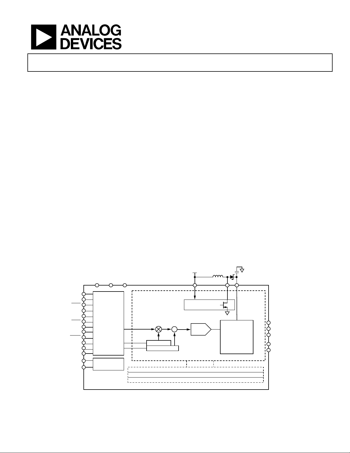
FUNCTIONAL BLOCK DIAGRAM
AV
SS
–15V/0V
DV
DD
DGND
LDAC
SCLK
SDIN
SYNC
SDO
CLEAR
FAULT
ALERT
AD1
AD0
REFOUT
REFIN
DIGITAL
INTERFACE
REFERENCE
AD5755-1
NOTES
1. x = A, B, C, AND D.
Rev. B
Information furnished by Analog Devices is believed to be accurate and reliable. However, no
responsibility is assumed by Analog Devices for its use, nor for any infringements of patents or other
rights of third parties that may result from its use. Specifications subject to change without notice. No
license is granted by implication or otherwise under any patent or patent rights of Analog Devices.
Trademarks and registered trademarks are the property of their respective owners.
AGND
AV
+15V
DD
GAIN REG A
OFFSET REG A
DAC CHANNEL A
DAC CHANNEL B
DAC CHANNEL C
DAC CHANNEL D
V
CC
5.0V
SW
DC-TO-DC
CONVERTER
+
DAC A
V
x
CURRENT AND
OUTPUT RANGE
BOOST_x
7.4V TO 29.5V
VOLTAGE
SCALING
I
OUT_x
R
SET_x
CHARTx
+V
SENSE_x
V
OUT _x
Figure 1.
One Technology Way, P.O. Box 9106, Norwood, MA 02062-9106, U.S.A.
Tel: 781.329.4700 www.analog.com
Fax: 781.461.3113 ©2011 Analog Devices, Inc. All rights reserved.
09226-101

AD5755-1 Data Sheet
TABLE OF CONTENTS
Features .............................................................................................. 1
Applications ....................................................................................... 1
General Description ......................................................................... 1
Product Highlights ........................................................................... 1
Companion Products ....................................................................... 1
Functional Block Diagram .............................................................. 1
Revision History ............................................................................... 3
Detailed Functional Block Diagram .............................................. 4
Specifications ..................................................................................... 5
AC Performance Characteristics ................................................ 8
Timing Characteristics ................................................................ 9
Absolute Maximum Ratings .......................................................... 12
ESD Caution ................................................................................ 12
Pin Configuration and Function Descriptions ........................... 13
Typ i cal Performance Characteristics ........................................... 16
Voltage Outputs .......................................................................... 16
Current Outputs ......................................................................... 20
DC-to-DC Block ......................................................................... 24
Reference ..................................................................................... 25
General ......................................................................................... 26
Terminology .................................................................................... 27
Theory of Operation ...................................................................... 29
DAC Architecture ....................................................................... 29
Power-On State of the AD5755-1 ............................................. 29
Serial Interface ............................................................................ 30
Transfer Function ....................................................................... 30
Registers ........................................................................................... 31
Programming Sequence to Write/Enable the Output
Correctly ...................................................................................... 32
Changing and Reprogramming the Range ............................. 32
Data Registers ............................................................................. 33
Control Registers ........................................................................ 35
Readback Operation .................................................................. 38
Device Features ............................................................................... 40
Output Fault ................................................................................ 40
Voltage Output Short-Circuit Protection ................................ 40
Digital Offset and Gain Control ............................................... 40
Status Readback During a Write .............................................. 40
Asynchronous Clear ................................................................... 41
Packet Error Checking ............................................................... 41
Watchdog Timer ......................................................................... 41
Output Alert ................................................................................ 41
Internal Reference ...................................................................... 41
External Current Setting Resistor ............................................ 41
HART ........................................................................................... 42
Digital Slew Rate Control .......................................................... 42
Power Dissipation control ......................................................... 43
DC-to-DC Converters ............................................................... 43
AICC Supply Requirements—Static .......................................... 44
AICC Supply Requirements—Slewing ...................................... 44
Applications Information .............................................................. 46
Voltage and Current Output Ranges on the Same Terminal 46
Current Output Mode with Internal R
Precision Voltage Reference Selection ..................................... 46
Driving Inductive Loads ............................................................ 47
Transient Voltage Protection .................................................... 47
Microprocessor Interfacing ....................................................... 47
Layout Guidelines....................................................................... 47
Galvanically Isolated Interface ................................................. 48
Outline Dimensions ....................................................................... 49
Ordering Guide .......................................................................... 49
................................ 46
SET
Rev. B | Page 2 of 52

Data Sheet AD5755-1
REVISION HISTORY
11/11—Rev. A to Rev. B
Removed Voltage Output Test Conditions/Comments, Table 1 .... 5
Changed Headroom and Footroom Test Conditions/Comments,
Table 1 .............................................................................................................. 5
Changes to Figure 4......................................................................... 10
Changes to Figure 5......................................................................... 11
Changes to SCLK Description, Table 5 ........................................ 13
Changes to Figure 12 ...................................................................... 16
Changes to Figure 21 ...................................................................... 18
Changes to Figure 37 ...................................................................... 20
Changes to Figure 44 ...................................................................... 22
Changes to Figure 71 ...................................................................... 29
Changes to Power-On State of the AD5755-1 Section ............... 30
Changes to Table 17 ........................................................................ 35
Changes to Readback Operation section and Table 26 .............. 38
Changes to Voltage Output Short-Circuit Protection Section .. 40
Changes to Figure 78 ...................................................................... 41
Changes to Figure 82 ...................................................................... 44
Changes to Figure 83, Figure 84, and Figure 85 .................................. 45
Changes to Transient Voltage Protection Section and Figure 86 ... 47
Changes to Galvanically Isolated Interface Section .................... 48
5/11—Rev. 0 to Rev. A
Removed Endnote 6 (Table 1) ......................................................... 6
Ch a n ged AV
Changed AI
Ch a n ged AV
Minimum Value from 10.8 V to 9 V ................... 6
DD
Minimum Value from −1.4 mA to −1.7 mA......... 7
SS
Voltage in Pin 19 Description ............................ 13
DD
Changes to Ordering Guide ........................................................... 48
4/11—Revision 0: Initial Version
Rev. B | Page 3 of 52
AD5755-1 Data Sheet
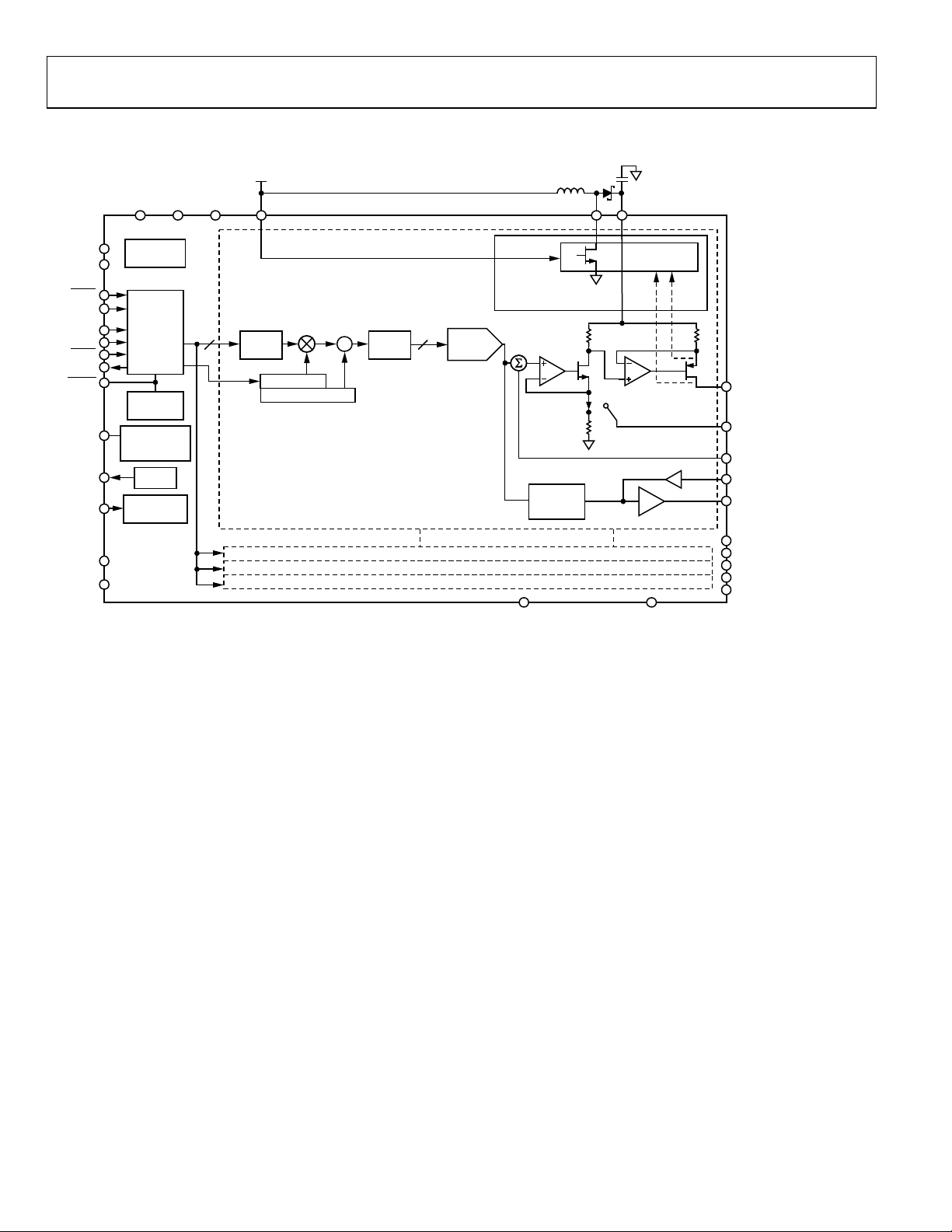
DETAILED FUNCTIONAL BLOCK DIAGRAM
AV
CC
5.0V
AV
SS
–15V/0V
AGND
AV
+15V
DD
SW
V
A
BOOST_A
DV
DGND
LDAC
CLEAR
SCLK
SDIN
SYNC
SDO
FAULT
ALERT
REFOUT
REFIN
AD1
AD0
DD
POWER-ON
RESET
INPUT
SHIFT
REGISTER
AND
CONTROL
STATUS
REGISTER
WATCHDOG
TIMER
(SPI ACTIVITY)
VREF
REFERENCE
BUFFERS
AD5755-1
16
INPUT
REG A
GAIN REG A
OFFSET REG A
DAC CHANNEL A
DAC CHANNEL B
DAC CHANNEL C
DAC CHANNEL D
DC-TO-DC
CONVERTER
V
REG
SEN1VSEN2
I
OUT_A
R
SET_A
POWER
CONTROL
16
DAC
+
REG A
DAC A
7.4V TO 29.5V
R2 R3
R1
CHARTA
+V
SENSE_A
V
OUT_A
I
, I
SET_B
SENSE_B
OUT_B
OUT_C
, R
,
V
SET_C
, +V
OUT_C
, I
OUT_D
, R
SENSE_
,
SET_D
V
OUT_D
, +V
C
OUT_B
R
CHARTB, CHARTC, CHARTD
+V
V
SENSE_
D
09226-001
RANGE
SCALING
SWB, SWC, SW
VOUT
V
BOOST_B,VBOOST_C,VBOOST_D
D
Figure 2.
Rev. B | Page 4 of 52

Data Sheet AD5755-1
Full-Scale TC2
±2 ppm FSR/°C
Differential Nonlinearity (DNL)
−1 +1
LSB
Guaranteed monotonic
DC PSRR
50 µV/V
SPECIFICATIONS
AVDD = V
GNDSW
otherwise noted.
Table 1.
Parameter1 Min Typ Max Unit Test Conditions/Comments
VOLTAGE OUTPUT
Output Voltage Ranges 0 5 V
0 10 V
−5 +5 V
−10 +10 V
0 6 V
0 12 V
−6 +6 V
−12 +12 V
ACCURACY BIPOLAR SUPPLY AVSS = −15 V, loaded and unloaded
Resolution 16 Bits
Total Unadjusted Error (TUE) −0.04 +0.04 % FSR
−0.03 ±0.0032 +0.03 % FSR TA = 25°C
TUE Long-Term Stability 35 ppm FSR Drift after 1000 hours, TJ = 150°C
Relative Accuracy (INL) −0.006 ±0.0012 +0.006 % FSR 0 V to 5 V, 0 V to 10 V, ±5 V, ±10 V ranges
−0.008 ±0.0012 +0.008 % FSR On overranges
Differential Nonlinearity (DNL) −1 +1 LSB Guaranteed monotonic
Zero-Scale Error −0.03 ±0.002 +0.03 % FSR
Zero-Scale TC2 ±2 ppm FSR/°C
Bipolar Zero Error −0.03 ±0.002 +0.03 % FSR
Bipolar Zero TC
Offset Error −0.03 ±0.002 +0.03 % FSR
Offset TC2 ±2 ppm FSR/°C
Gain Error −0.03 ±0.004 +0.03 % FSR
Gain TC2 ±3 ppm FSR/°C
Full-Scale Error −0.03 ±0.002 +0.03 % FSR
= 15 V; AVSS = −15 V/0 V; DVDD = 2.7 V to 5.5 V; AVCC = 4.5 V to 5.5 V; dc-to-dc converter disabled; AGND = DGND =
BOOST_x
= 0 V; REFIN = 5 V; voltage outputs: RL = 1 kΩ, CL = 220 pF; current outputs: RL = 300 Ω; all specifications T
x
2
±1 ppm FSR/°C
MIN
to T
MAX
, unless
ACCURACY UNIPOLAR SUPPLY2 AVSS = 0 V
Total Unadjusted Error (TUE) −0.06 ±0.025 +0.06 % FSR
Relative Accuracy (INL)3 −0.009 +0.009 % FSR
Zero-Scale Error +0.22 % FSR
Offset Error −0.07 ±0.025 +0.07 % FSR
Gain Error −0.07 ±0.015 +0.07 % FSR
Full-Scale Error −0.06 ±0.015 +0.06 % FSR
OUTPUT CHARACTERISTICS2
Headroom 1 2.2 V
Footroom 0.7 1.4 V
Output Voltage Drift vs. Time 20 ppm FSR Drift after 1000 hours, ¾ scale output, TJ = 150°C,
Short-Circuit Current 12/6 16/8 mA Programmable by user, defaults to 16 mA typical
Load 1 kΩ For specified performance
Capacitive Load Stability 10 nF
2 µF External compensation capacitor of 220 pF connected
DC Output Impedance 0.06 Ω
DC Crosstalk 24 µV
Rev. B | Page 5 of 52
With respect to V
BOOST
supply
With respect to the AVSS supply, bipolar output
ranges
= −15 V
AV
SS
level

AD5755-1 Data Sheet
Gain Error
−0.05
±0.004
+0.05
% FSR
Offset Error Drift2
±6 ppm FSR/°C
Gain TC2
±9 ppm FSR/°C
Parameter1 Min Typ Max Unit Test Conditions/Comments
CURRENT OUTPUT
Output Current Ranges 0 24 mA
0 20 mA
4 20 mA
Resolution 16 Bits
ACCURACY (EXTERNAL R
)
SET
Total Unadjusted Error (TUE) −0.05 ±0.009 +0.05 % FSR
TUE Long-Term Stability 100 ppm FSR Drift after 1000 hours, TJ = 150°C
Relative Accuracy (INL) −0.006 +0.006 % FSR
Differential Nonlinearity (DNL) −1 +1 LSB Guaranteed monotonic
Offset Error −0.05 ±0.005 +0.05 % FSR
Offset Error Drift2 ±4 ppm FSR/°C
Gain TC2 ±3 ppm FSR/°C
Full-Scale Error −0.05 ±0.008 +0.05 % FSR
Full-Scale TC2 ±5 ppm FSR/°C
DC Crosstalk 0.0005 % FSR External R
ACCURACY (INTERNAL R
Total Unadjusted Error (TUE)
)
SET
4, 5
−0.14 +0.14 % FSR
−0.11 ±0.009 +0.11 % FSR TA = 25°C
TUE Long-Term Stability 180 ppm FSR Drift after 1000 hours, TJ = 150°C
Relative Accuracy (INL) −0.006 +0.006 % FSR
Relative Accuracy (INL) −0.004 +0.004 % FSR TA = 25°C
Differential Nonlinearity (DNL) −1 +1 LSB Guaranteed monotonic
Offset Error
4, 5
−0.05 +0.05 % FSR
−0.04 ±0.007 +0.04 % FSR TA = 25°C
Assumes ideal resistor, see the External Current Setting
Resistor section for more information
SET
Gain Error −0.12 +0.12 % FSR
−0.06 ±0.002 +0.06 % FSR TA = 25°C
Full-Scale Error
4, 5
−0.14 +0.14 % FSR
−0.1 ±0.007 +0.1 % FSR TA = 25°C
Full-Scale TC2 ±14 ppm FSR/°C
DC Crosstalk5 −0.011 % FSR Internal R
SET
OUTPUT CHARACTERISTICS2
Current Loop Compliance Voltage V
BOOST_x
2.4
−
V
BOOST_x
2.7
−
V
Output Current Drift vs. Time Drift after 1000 hours, ¾ scale output, TJ = 150°C
90 ppm FSR External R
140 ppm FSR Internal R
SET
SET
Resistive Load 1000 Ω The dc-to-dc converter has been characterized with
a maximum load of 1 kΩ, chosen such that compliance is not exceeded; see
MaxV bits in
Tab le 25
Figure 53 and DC-DC
Output Impedance 100 MΩ
DC PSRR 0.02 1 µA/V
Rev. B | Page 6 of 52

Data Sheet AD5755-1
Output Noise (0.1 Hz to 10 Hz)2
7
µV p-p
VOL, Output Low Voltage
0.6 V
At 2.5 mA
Parameter1 Min Typ Max Unit Test Conditions/Comments
REFERENCE INPUT/OUTPUT
Reference Input2
Reference Input Voltage 4.95 5 5.05 V For specified performance
DC Input Impedance 45 150 MΩ
Reference Output
Output Voltage 4.995 5 5.005 V TA = 25°C
Reference TC2 −10 ±5 +10 ppm/°C
Noise Spectral Density2 100 nV/√Hz At 10 kHz
Output Voltage Drift vs. Time2 180 ppm Drift after 1000 hours, TJ = 150°C
Capacitive Load2 1000 nF
Load Current 9 mA
Short-Circuit Current 10 mA
Line Regulation2 3 ppm/V
Load Regulation2 95 ppm/mA
Thermal Hysteresis2 160 ppm First temperature cycle
5 ppm Second temperature cycle
DC-TO-DC
Switch
Switch On Resistance 0.425 Ω
Switch Leakage Current 10 nA
Peak Current Limit 0.8 A
Oscillator
Oscillator Frequency 11.5 13 14.5 MHz This oscillator is divided down to give the dc-to-dc
Maximum Duty Cycle 89.6 % At 410 kHz dc-to-dc switching frequency
DIGITAL INPUTS2 JEDEC compliant
VIH, Input High Voltage 2 V
VIL, Input Low Voltage 0.8 V
Input Current −1 +1 µA Per pin
Pin Capacitance 2.6 pF Per pin
DIGITAL OUTPUTS2
SDO, ALERT
VOL, Output Low Voltage 0.4 V Sinking 200 µA
VOH, Output High Voltage DVDD − 0.5 V Sourcing 200 µA
High Impedance Leakage
Current
High Impedance Output
Capacitance
FAULT
VOL, Output Low Voltage 0.4 V 10 kΩ pull-up resistor to DVDD
−1 +1 µA
2.5 pF
See
Figure 64
See
Figure 65
See
Figure 64
converter switching frequency
VOH, Output High Voltage 3.6 V 10 kΩ pull-up resistor to DVDD
POWER REQUIREMENTS
AVDD 9 33 V
AVSS −26.4 −10.8/0 V
DVDD 2.7 5.5 V
AVCC 4.5 5.5 V
Rev. B | Page 7 of 52

AD5755-1 Data Sheet
Power Dissipation
173 mW
AVDD = +15 V, AVSS = −15 V, dc-to-dc converter
Digital Feedthrough
1
nV-sec
AC PSRR
83 dB
200 mV 50 Hz/60 Hz sine wave superimposed on power
Output Noise Spectral Density
0.5 nA/√Hz
Measured at 10 kHz, midscale output, 0 mA to 24 mA
Parameter1 Min Typ Max Unit Test Conditions/Comments
AIDD 8.6 10.5 mA Voltage output mode on all channels, output
7 7.5 mA Current output mode on all channels
AISS −11 −8.8 mA Voltage output mode on all channels, output
−1.7 mA Current output mode on all channels
DICC 9.2 11 mA VIH = DVDD, VIL = DGND, internal oscillator running,
AICC 1 mA Output unloaded, over supplies
I
2.7 mA Per channel, voltage output mode, output
BOOST
6
I
1 mA Per channel, current output mode, 0 mA output
BOOST
1
Temperature range: −40°C to +105°C; typical at +25°C.
2
Guaranteed by design and characterization; not production tested.
3
For voltage output ranges in unipolar supply mode, the INL and TUE are measured beginning from Code 4096.
4
For current outputs with internal R
loaded with the same code.
5
See the Current Output Mode with Internal R
6
Efficiency plots in Figure 55, Figure 56, Figure 57, and Figure 58 include the I
, the offset, full-scale, and TUE measurements exclude dc crosstalk. The measurements are made with all four channels enabled
SET
section for more explanation of the dc crosstalk.
SET
quiescent current
BOOST
AC PERFORMANCE CHARACTERISTICS
AVDD = V
GNDSW
otherwise noted.
= 15 V; AVSS = −15 V; DVDD = 2.7 V to 5.5 V; AVCC = 4.5 V to 5.5 V; dc-to-dc converter disabled; AGND = DGND =
BOOST_x
= 0 V; REFIN = 5 V; voltage outputs: RL = 2 kΩ, CL = 220 pF; current outputs: RL = 300 Ω; all specifications T
x
unloaded, over supplies
unloaded, over supplies
over supplies
unloaded, over supplies
enable, current output mode, outputs disabled
MIN
to T
MAX
, unless
Table 2.
Parameter1 Min Typ Max Unit Test Conditions/Comments
DYNAMIC PERFORMANCE
Voltage Output
Output Voltage Settling Time 11 µs 5 V step to ±0.03% FSR, 0 V to 5 V range
18 µs 10 V step to ±0.03% FSR, 0 V to 10 V range
13 µs 100 mV step to 1 LSB (16-bit LSB), 0 V to 10 V range
Slew Rate 1.9 V/µs 0 V to 10 V range
Power-On Glitch Energy 150 nV-sec
Digital-to-Analog Glitch Energy 6 nV-sec
Glitch Impulse Peak Amplitude 25 mV
DAC to DAC Crosstalk 2 nV-sec 0 V to 10 V range
Output Noise (0.1 Hz to 10 Hz
Bandwidth)
Output Noise Spectral Density 150 nV/√Hz Measured at 10 kHz, midscale output, 0 V to 10 V range
Current Output
Output Current Settling Time 15 µs To 0.1% FSR (0 mA to 24 mA)
See test conditions/
Output Noise (0.1 Hz to 10 Hz
Bandwidth)
1
Guaranteed by design and characterization; not production tested.
0.15 LSB p-p 16-bit LSB, 0 V to 10 V range
supply voltage
ms
See
Figure 49, Figure 50, and Figure 51
comments
0.15 LSB p-p 16-bit LSB, 0 mA to 24 mA range
range
Rev. B | Page 8 of 52
Data Sheet AD5755-1
t17
500
ns min
falling edge to
rising edge
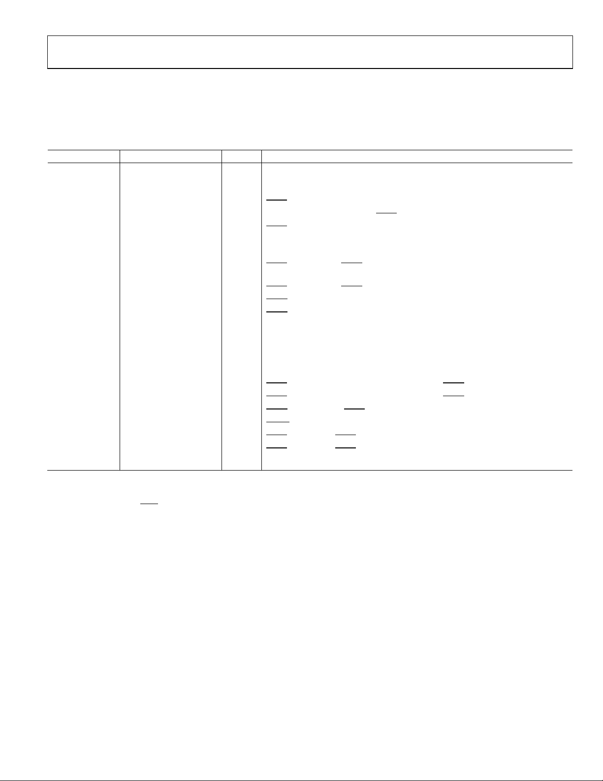
TIMING CHARACTERISTICS
AVDD = V
GNDSW
otherwise noted.
= 15 V; AVSS = −15 V; DVDD = 2.7 V to 5.5 V; AVCC = 4.5 V to 5.5 V; dc-to-dc converter disabled; AGND = DGND =
BOOST_x
= 0 V; REFIN = 5 V; voltage outputs: RL = 1 kΩ, CL = 220 pF; current outputs: RL = 300 Ω; all specifications T
x
MIN
to T
MAX
, unless
Table 3.
Parameter
1, 2, 3
Limit at T
, T
Unit Description
MIN
MAX
t1 33 ns min SCLK cycle time
t2 13 ns min SCLK high time
t3 13 ns min SCLK low time
t4 13 ns min
falling edge to SCLK falling edge setup time
SYNC
t5 13 ns min 24th/32nd SCLK falling edge to
t6 198 ns min
SYNC
high time
t7 5 ns min Data setup time
t8 5 ns min Data hold time
t9 20 µs min
rising edge to
SYNC
falling edge (all DACs updated or any channel has
LDAC
digital slew rate control enabled)
5 µs min
t10 10 ns min
t11 500 ns max
t12 See the AC Performance
µs max DAC output settling time
rising edge to
SYNC
pulse width low
LDAC
falling edge to DAC output response time
LDAC
falling edge (single DAC updated)
LDAC
Characteristics section
t13 10 ns min CLEAR high time
t14 5 µs max CLEAR activation time
t15 40 ns max SCLK rising edge to SDO valid
t16 21 µs min
5 µs min
t18 800 ns min
4
t
20 µs min
19
5 µs min
rising edge to DAC output response time (
SYNC
rising edge to DAC output response time (
SYNC
LDAC
RESET
high to next
SYNC
high to next
SYNC
pulse width
SYNC
low (digital slew rate control enabled) (all DACs updated)
SYNC
low (digital slew rate control disabled) (single DAC
SYNC
updated)
1
Guaranteed by design and characterization; not production tested.
2
All input signals are specified with tR = tF = 5 ns (10% to 90% of DVDD) and timed from a voltage level of 1.2 V.
3
See Figure 3, Figure 4, Figure 5, and Figure 6.
4
This specification applies if
LDAC
is held low during the write cycle; otherwise, see t9.
rising edge (see Figure 78)
SYNC
LDAC
LDAC
= 0) (all DACs updated)
= 0) (single DAC updated)
Rev. B | Page 9 of 52
AD5755-1 Data Sheet
S
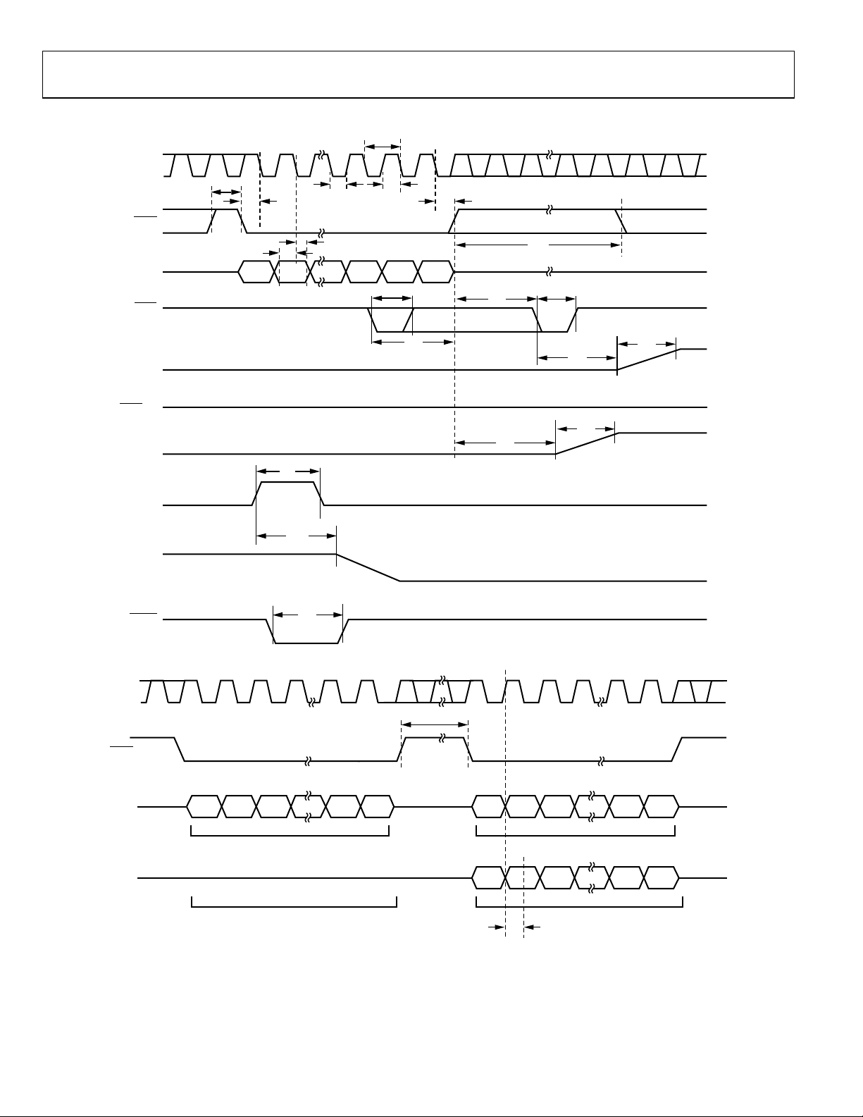
Timing Diagrams
t
1
SCLK
SYNC
SDIN
LDAC
V
OUT_x
LDAC = 0
V
OUT_x
CLEAR
V
OUT_x
12 24
t
6
t
4
t
7
MSB
t
13
t
t
3
t
8
14
t
2
t
10
t
5
t
19
LSB
t
t
9
t
17
t
16
10
t
t
11
t
12
12
SCLK
YNC
SDIN
SDO
RESET
t
18
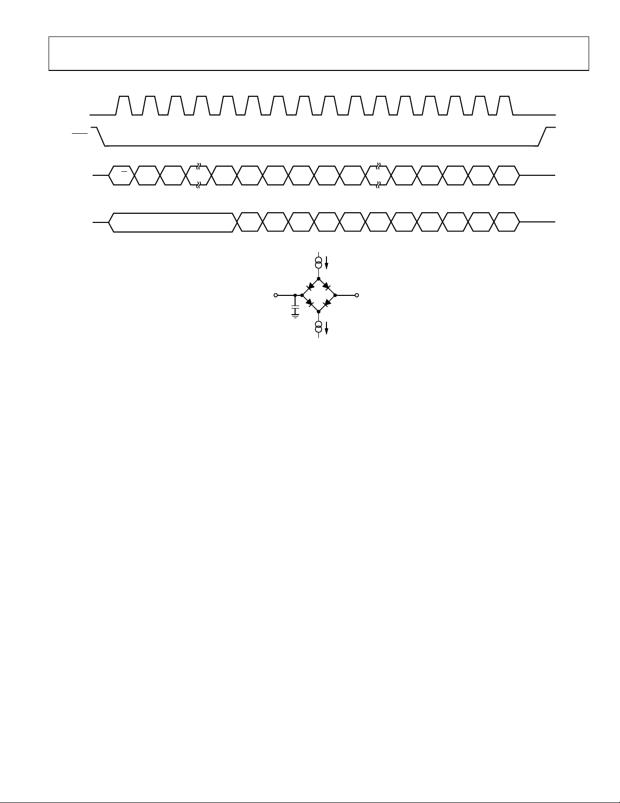
Figure 3. Serial Interface Timing Diagram
1 1
MSB MSBLSB LSB
INPUT WORD SPECIFIES
REGISTER TO BE READ
UNDEFINED SELECTED REGISTER DATA
24 24
t
6
NOP CONDITION
MSB LSB
t
15
CLOCKED OUT
Figure 4. Readback Timing Diagram
09226-002
9226-003
Rev. B | Page 10 of 52
Data Sheet AD5755-1
SDO DISABL E D
R/W
SDIN
SCLK
SYNC
SDO
1 2 16
LSB MSB
DUT_
AD1
SDO_
ENAB
DUT_
AD0
X X X D15 D14 D1 D0
STATUSSTATUSSTATUSSTATUS
09226-004
200µA I
OL
200µA I
OH
V
OH
(MIN) OR
V
OL
(MAX)
TO OUTPUT
PIN
C
L
50pF
09226-005
Figure 5. Status Readback During Write
Figure 6. Load Circuit for SDO Timing Diagram
Rev. B | Page 11 of 52
AD5755-1 Data Sheet
AVSS to AGND, DGND
+0.3 V to −28 V
DVDD to DGND
−0.3 V to +7 V
(whichever is less)
REFIN, REFOUT to AGND
−0.3 V to AVDD + 0.3 V or +7 V
Junction Temperature (TJ max)
125°C
Lead Temperature
JEDEC industry standard
ABSOLUTE MAXIMUM RATINGS
TA = 25°C, unless otherwise noted. Transient currents of up to
100 mA do not cause SCR latch-up.
Table 4.
Parameter Rating
AVDD, V
AVDD to AVSS −0.3 V to +60 V
AVCC to AGND −0.3 V to +7 V
to AGND, DGND −0.3 V to +33 V
BOOST_x
Stresses above those listed under Absolute Maximum Ratings
may cause permanent damage to the device. This is a stress
rating only; functional operation of the device at these or any
other conditions above those indicated in the operational
section of this specification is not implied. Exposure to absolute
maximum rating conditions for extended periods may affect
device reliability.
ESD CAUTION
Digital Inputs to DGND −0.3 V to DVDD + 0.3 V or +7 V
(whichever is less)
Digital Outputs to DGND −0.3 V to DVDD + 0.3 V or +7 V
(whichever is less)
V
to AGND AVSS to V
OUT_x
or 33 V if using
BOOST_x
the dc-to-dc circuitry
+V
to AGND AVSS to V
SENSE_x
or 33 V if using
BOOST_x
the dc-to-dc circuitry
I
to AGND AVSS to V
OUT_x
or 33 V if using
BOOST_x
the dc-to-dc circuitry
SWx to AGND −0.3 to +33 V
AGND, GNDSWx to DGND −0.3 V to +0.3 V
Operating Temperature Range (TA)
Industrial1 −40°C to +105°C
Storage Temperature Range −65°C to +150°C
64-Lead LFCSP
θJA Thermal Impedance2 20°C/W
Power Dissipation (TJ max − TA)/θJA
Soldering J-STD-020
1
Power dissipated on chip must be derated to keep the junction temperature
below 125°C.
2
Based on a JEDEC 4-layer test board.
Rev. B | Page 12 of 52
Data Sheet AD5755-1
PIN CONFIGURATION AND FUNCTION DESCRIPTIONS
LV_D
PIN 1
INDICATOR
DCDC_D
SET_CRSET_D
R
646362616059585756555453525150
SENSE_D
REFOUT
REFIN
COMP
CHARTD
+V
COMP
BOOST_DVOUT_D
V
LV_C
SENSE_C
OUT_D
I
AVSSCOMP
OUT_C
CHARTC
+V
V
49
1
R
SET_B
R
2
SET_A
REFGND
REFGND
NOTES
1. THE EXPOSED PAD SHOULD BE CONNECTED TO THE POTENTIAL OF
THE AV
UNCONNECTED . IT I S RE C OMMENDED T H AT THE PAD BE THERMALL Y
CONNECTED TO A COPPER PLANE FOR ENHANCED THERMAL PERFORM ANCE .
3
4
AD0
5
AD1
6
SYNC
7
SCLK
8
SDIN
9
SDO
10
DV
11
DD
DGND
12
LDAC
13
CLEAR
14
ALERT
15
FAULT
16
171819202122232425262728293031
POC
PIN, O R, ALTERNATIVELY, IT CAN BE LEFT E LECTRICA LLY
SS
RESET
DD
LV_A
AV
COMP
AD5755-1
TOP VIEW
(Not to Scale)
DCDC_A
V
SENSE_A
BOOST_A
CHARTA
V
+V
COMP
OUT_AIOUT_A
SS
LV_B
AV
CHARTB
COMP
V
SENSE_B
+V
48
COMP
DCDC_C
I
47
OUT_C
V
46
BOOST_C
AV
45
CC
SW
44
C
43
GNDSW
GNDSW
SW
D
AV
SS
SW
A
GNDSW
GNDSW
SW
B
AGND
V
BOOST_B
I
OUT_B
C
D
A
B
09266-006
42
41
40
39
38
37
36
35
34
33
32
OUT_B
DCDC_B
COMP
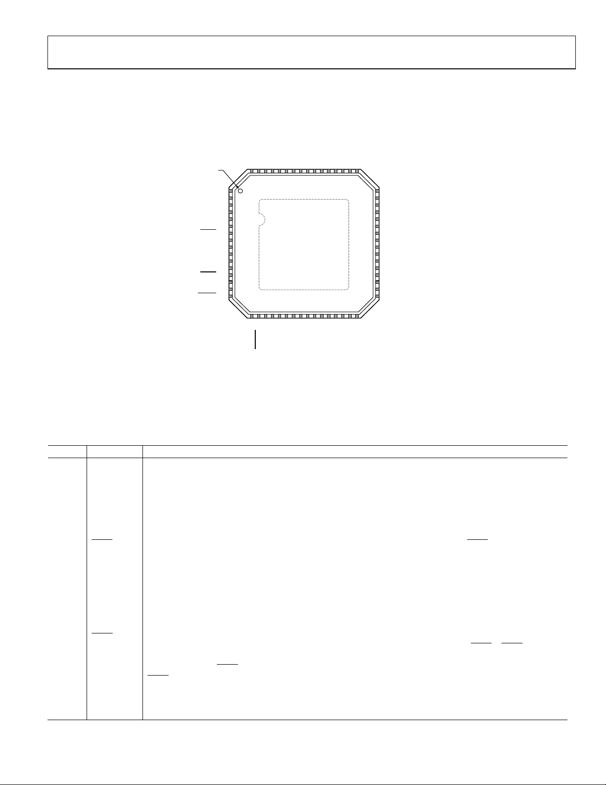
Figure 7. Pin Configuration
Table 5. Pin Function Descriptions
Pin No. Mnemonic Description
1 R
SET_B
An external, precision, low drift 15 kΩ current setting resistor can be connected to this pin to improve the I
temperature drift performance. See the Device Features section.
2 R
SET_A
An external, precision, low drift 15 kΩ current setting resistor can be connected to this pin to improve the I
temperature drift performance. See the Device Features section.
3, 4 REFGND Ground Reference Point for Internal Reference.
5 AD0 Address Decode for the Device Under Test (DUT) on the Board.
6 AD1 Address Decode for the DUT on the Board.
7
Active Low Input. This is the frame synchronization signal for the serial interface. While SYNC is low, data is
SYNC
transferred in on the falling edge of SCLK.
8 SCLK
Serial Clock Input. Data is clocked into the input shift register on the falling edge of SCLK. This operates at clock
speeds of up to 30 MHz.
9 SDIN Serial Data Input. Data must be valid on the falling edge of SCLK.
10 SDO Serial Data Output. Used to clock data from the serial register in readback mode. See Figure 4 and Figure 5.
11 DVDD Digital Supply. The voltage range is from 2.7 V to 5.5 V.
12 DGND Digital Ground.
13
Load DAC, Active Low Input. This is used to update the DAC register and consequently the DAC outputs. When
LDAC
tied permanently low, the addressed DAC data register is updated on the rising edge of SYNC
. If LDAC is held
high during the write cycle, the DAC input register is updated, but the DAC output update only takes place at
14 CLEAR
the falling edge of LDAC
LDAC
pin must not be left unconnected.
Active High, Edge Sensitive Input. Asserting this pin sets the output current and voltage to the preprogrammed
(see Figure 3). Using this mode, all analog outputs can be updated simultaneously. The
clear code bit setting. Only channels enabled to be cleared are cleared. See the Device Features section for more
information. When CLEAR is active, the DAC output register cannot be written to.
OUT_B
OUT_A
Rev. B | Page 13 of 52
AD5755-1 Data Sheet
19
AVDD
Positive Analog Supply. The voltage range is from 9 V to 33 V.
36
SWB
Switching Output for Channel B DC-to-DC Circuitry. To use the dc-to-dc feature of the device, connect as shown
in Figure 80.
Pin No. Mnemonic Description
15 ALERT Active High Output. This pin is asserted when there has been no SPI activity on the interface pins for a
predetermined time. See the Device Features section for more information.
16
FAULT
17 POC Power-On Condition. This pin determines the power-on condition and is read during power-on or, alternatively,
18
RESET
Active Low Output. This pin is asserted low when an open circuit in current mode is detected, a short circuit in
voltage mode is detected, a PEC error is detected, or an overtemperature is detected (see the Device Features
section). Open-drain output.
after a device reset. If POC = 0, the device is powered up with the voltage and current channels in tristate mode.
If POC = 1, the device is powered up with a 30 kΩ pull-down resistor to ground on the voltage output channel,
and the current channel is in tristate mode.
Hardware Reset, Active Low Input.
20 COMP
Optional Compensation Capacitor Connection for V
LV_ A
this pin and the V
pin allows the voltage output to drive up to 2 µF. Note that the addition of this capacitor
OUT_A
Output Buffer. Connecting a 220 pF capacitor between
OUT_A
reduces the bandwidth of the output amplifier, increasing the settling time.
21 CHARTA HART Input Connection for DAC Channel A.
22 +V
23 COMP
Sense Connection for the Positive Voltage Output Load Connection for V
SENSE_A
DC-to-DC Compensation Capacitor. Connect a 10 nF capacitor from this pin to ground. Used to regulate the
DCDC_A
OUT_A
feedback loop of the Channel A dc-to-dc converter. Alternatively, if using an external compensation resistor,
place a resistor in series with a capacitor to ground from this pin (see the DC-to-DC Converter Compensation
Capacitors and the AI
Supply Requirements—Slewing sections in the Device Features section for more
CC
information).
24 V
Supply for Channel A Current Output Stage (see Figure 73). This is also the supply for the V
BOOST_A
regulated to 15 V by the dc-to-dc converter. To use the dc-to-dc feature of the device, connect as shown in
Figure 80.
25 V
26 I
Buffered Analog Output Voltage for DAC Channel A.
OUT_A
Current Output Pin for DAC Channel A.
OUT_A
27 AVSS Negative Analog Supply. Voltage range is from −10.8 V to −26.4 V.
28 COMP
Optional Compensation Capacitor Connection for V
LV_ B
this pin and the V
pin allows the voltage output to drive up to 2 µF. Note that the addition of this capacitor
OUT_B
Output Buffer. Connecting a 220 pF capacitor between
OUT_B
reduces the bandwidth of the output amplifier, increasing the settling time.
29 CHARTB HART Input Connection for DAC Channel B.
30 +V
31 V
32 COMP
Sense Connection for the Positive Voltage Output Load Connection for V
SENSE_B
Buffered Analog Output Voltage for DAC Channel B.
OUT_B
DC-to-DC Compensation Capacitor. Connect a 10 nF capacitor from this pin to ground. Used to regulate the
DCDC_B
OUT_B
feedback loop of the Channel B dc-to-dc converter. Alternatively, if using an external compensation resistor,
place a resistor in series with a capacitor to ground from this pin (see the DC-to-DC Converter Compensation
Capacitors and AI
Supply Requirements—Slewing sections in the Device Features section for more
CC
information).
33 I
34 V
Current Output Pin for DAC Channel B.
OUT_B
Supply for Channel B Current Output Stage (see Figure 73). This is also the supply for the V
BOOST_B
regulated to 15 V by the dc-to-dc converter. To use the dc-to-dc feature of the device, connect as shown in
Figure 80.
35 AGND Ground Reference Point for Analog Circuitry. This must be connected to 0 V.
.
stage, which is
OUT_x
.
stage, which is
OUT_x
in Figure 80.
37 GNDSWB Ground Connection for DC-to-DC Switching Circuit. This pin should always be connected to ground.
38 GNDSWA Ground Connection for DC-to-DC Switching Circuit. This pin should always be connected to ground.
39 SWA Switching Output for Channel A DC-to-DC Circuitry. To use the dc-to-dc feature of the device, connect as shown
40 AVSS Negative Analog Supply Pin. The voltage range is from −10.8 V to −26.4 V. This pin can be connected to 0 V if
using the device in unipolar supply mode.
41 SWD Switching Output for Channel D DC-DC Circuitry. To use the dc-to-dc feature of the device, connect as shown in
Figure 80.
42 GNDSWD Ground Connections for DC-to-DC Switching Circuit. This pin should always be connected to ground.
43 GNDSWC Ground Connections for DC-to-DC Switching Circuit. This pin should always be connected to ground.
44 SWC Switching Output for Channel C DC-to-DC Circuitry. To use the dc-to-dc feature of the device, connect as shown
in Figure 80.
45 AVCC Supply for DC-to-DC Circuitry.
Rev. B | Page 14 of 52

Data Sheet AD5755-1
48
COMP
DC-to-DC Compensation Capacitor. Connect a 10 nF capacitor from this pin to ground. Used to regulate the
62
REFOUT
Internal Reference Voltage Output. It is recommended to place a 0.1 µF capacitor between REFOUT and
Pin No. Mnemonic Description
46 V
47 I
49 V
50 +V
51 CHARTC HART Input Connection for DAC Channel C.
52 COMP
53 AVSS Negative Analog Supply Pin.
54 I
55 V
56 V
57 COMP
58 +V
59 CHARTD HART Input Connection for DAC Channel D
60 COMP
61 REFIN External Reference Voltage Input.
Supply for Channel C Current Output Stage (see Figure 73). This is also the supply for the V
BOOST_C
regulated to 15 V by the dc-to-dc converter. To use the dc-to-dc feature of the device, connect as shown in
Figure 80.
Current Output Pin for DAC Channel C.
OUT_C
DCDC_C
feedback loop of the Channel C dc-to-dc converter. Alternatively, if using an external compensation resistor,
place a resistor in series with a capacitor to ground from this pin (see the
DC-to-DC Converter Compensation
Capacitors and AICC Supply Requirements—Slewing sections in the Device Features section for more
information).
Buffered Analog Output Voltage for DAC Channel C.
OUT_C
Sense Connection for the Positive Voltage Output Load Connection for V
SENSE_C
Optional Compensation Capacitor Connection for V
LV_ C
this pin and the V
pin allows the voltage output to drive up to 2 µF. Note that the addition of this capacitor
OUT_C
Output Buffer. Connecting a 220 pF capacitor between
OUT_C
OUT_C
reduces the bandwidth of the output amplifier, increasing the settling time.
Current Output Pin for DAC Channel D.
OUT_D
Buffered Analog Output Voltage for DAC Channel D.
OUT_D
Supply for Channel D Current Output Stage (see Figure 73). This is also the supply for the V
BOOST_D
regulated to 15 V by the dc-to-dc converter. To use the dc-to-dc feature of the device, connect as shown in
Figure 80.
DC-to-DC Compensation Capacitor. Connect a 10 nF capacitor from this pin to ground. Used to regulate the
DCDC_D
feedback loop of the Channel D dc-to-dc converter. Alternatively, if using an external compensation resistor,
place a resistor in series with a capacitor to ground from this pin (see the DC-to-DC Converter Compensation
Capacitors and AI
Supply Requirements—Slewing sections in the Device Features section for more
CC
information).
Sense Connection for the Positive Voltage Output Load Connection for V
SENSE_D
Optional Compensation Capacitor Connection for V
LV_ D
this pin and the V
pin allows the voltage output to drive up to 2 µF. Note that the addition of this capacitor
OUT_D
Output Buffer. Connecting a 220 pF capacitor between
OUT_D
OUT_D
reduces the bandwidth of the output amplifier, increasing the settling time.
stage, which is
OUT_x
.
stage, which is
OUT_x
.
REFGND.
63 R
An external, precision, low drift 15 kΩ current setting resistor can be connected to this pin to improve the I
SET_D
temperature drift performance. See the Device Features section.
64 R
An external, precision, low drift 15 kΩ current setting resistor can be connected to this pin to improve the I
SET_C
temperature drift performance. See the Device Features section.
EPAD Exposed Pad. This exposed pad should be connected to the potential of the AVSS pin, or, alternatively, it can be
left electrically unconnected. It is recommended that the pad be thermally connected to a copper plane for
enhanced thermal performance.
Rev. B | Page 15 of 52
OUT_D
OUT_C
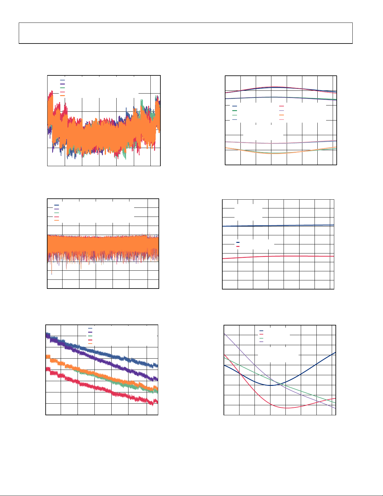
AD5755-1 Data Sheet
0.0015
0.0010
0.0005
0
–0.0005
–0.0010
0 10k 20k 30k 40k 50k 60k
INL ERROR ( %FSR)
CODE
09226-023
±10V RANGE
±5V RANGE
+10V RANGE
+5V RANGE
+10V RANGE WITH DCDC
AV
DD
= +15V
AV
SS
= –15V
T
A
= 25°C
–1.0
–0.8
–0.6
–0.4
–0.2
0
0.2
0.4
0.6
0.8
1.0
0 10k 20k 30k 40k 50k 60k
DNL ERROR (LSB)
CODE
±10V RANGE
±5V RANGE
+10V RANGE
+5V RANGE
+10V RANGE WI TH DCDC
AV
DD
= +15V
AV
SS
= –15V
T
A
= 25°C
09226-024
10k 20k 30k 40k 50k 60k
–0.010
–0.008
–0.006
–0.004
–0.002
0
0.002
0.004
0.006
0
TOTAL UNADJUSTED ERROR (%FSR)
CODE
±10V RANGE
±5V RANGE
+10V RANGE
+5V RANGE
+10V RANGE WI TH DCDC
AV
DD
= +15V
AV
SS
= –15V
T
A
= 25°C
09226-025
–0.0015
–0.0010
–0.0005
0
0.0005
0.0010
0.0015
–40 –20 0 20 40 60 80 100
INL ERROR ( %FSR)
TEMPERATURE (°C)
+5V RANGE MAX I NL +10V RANGE MAX INL
±5V RANGE MAX I NL ±10V RANGE MAX INL
+5V RANGE MIN INL +10V RANGE MI N INL
±5V RANGE MIN INL
±10V RANGE MIN INL
AV
DD
= +15V
AV
SS
= –15V
OUTPUT UNLOADED
09226-127
–1.0
–0.8
–0.6
–0.4
–0.2
0
0.2
0.4
0.6
0.8
1.0
–40 –20 0 20 40 60 80 100
DNL ERROR (L S B)
TEMPERATURE (°C)
AVDD = +15V
AV
SS
= –15V
ALL RANGES
DNL ERROR MAX
DNL ERROR MI N
09226-128
–0.006
–0.004
–0.002
0
0.002
0.004
0.006
0.008
0.010
0.012
–40 –20 0 20 40 60 80 100
TOTAL UNADJUSTED ERROR ( %FSR)
TEMPERATURE (°C)
AVDD = +15V
AV
SS
= –15V
OUTPUT UNLOADED
+5V RANGE
+10V RANGE
±5V RANGE
±10V RANGE
09226-129
TYPICAL PERFORMANCE CHARACTERISTICS
VOLTAGE OUTPUTS
Figure 8. Integral Nonlinearity Error vs. DAC Code
Figure 9. Differential Nonlinearity Error vs. DAC Code
Figure 11. Integral Nonlinearity Error vs. Temperature
Figure 12. Differential Nonlinearity Error vs. Temperature
Figure 10. Total Unadjusted Error vs. DAC Code
Figure 13. Total Unadjusted Error vs. Temperature
Rev. B | Page 16 of 52
 Loading...