Complete, Quad, 12-/14-/16-Bit, Serial Input,
A
A
FEATURES
Complete, quad, 12-/14-/16-bit digital-to-analog converter
(DAC)
Operates from single/dual supplies
Software programmable output range
+5 V, +10 V, +10.8 V, ±5 V, ±10 V, ±10.8 V
INL error: ±16 LSB maximum, DNL error: ±1 LSB maximum
Total unadjusted error (TUE): 0.1% FSR maximum
Settling time: 10 μs typical
Integrated reference buffers
Output control during power-up/brownout
Simultaneous updating via
Asynchronous
to zero scale or midscale
CLR
DSP-/microcontroller-compatible serial interface
24-lead TSSOP
Operating temperature range: −40°C to +85°C
iCMOS process technology
APPLICATIONS
Industrial automation
Closed-loop servo control, process control
Automotive test and measurement
Programmable logic controllers
LDAC
1
Unipolar/Bipolar Voltage Output DACs
AD5724/AD5734/AD5754
GENERAL DESCRIPTION
The AD5724/AD5734/AD5754 are quad, 12-/14-/16-bit, serial
input, voltage output digital-to-analog converters. They operate
from single-supply voltages from +4.5 V up to +16.5 V or dualsupply voltages from ±4.5 V up to ±16.5 V. Nominal full-scale
output range is software-selectable from +5 V, +10 V, +10.8 V,
±5 V, ±10 V, or ±10.8 V. Integrated output amplifiers, reference
buffers, and proprietary power-up/power-down control circuitry
are also provided.
The parts offer guaranteed monotonicity, integral nonlinearity
(INL) of ±16 LSB maximum, low noise, and 10 μs maximum
settling time.
The AD5724/AD5734/AD5754 use a serial interface that operates
at clock rates up to 30 MHz and are compatible with DSP and
microcontroller interface standards. Double buffering allows
the simultaneous updating of all DACs. The input coding is
user-selectable twos complement or offset binary for a bipolar
output (depending on the state of Pin BIN/
binary for a unipolar output. The asynchronous clear function
clears all DAC registers to a user-selectable zero-scale or midscale
output. The parts are available in a 24-lead TSSOP and offer
guaranteed specifications over the −40°C to +85°C industrial
temperature range.
2sComp
), and straight
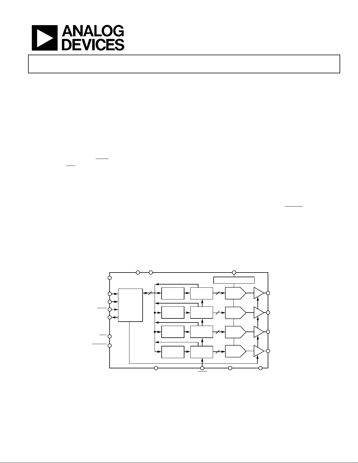
FUNCTIONAL BLOCK DIAGRAM
V
AV
DD
SS
DV
CC
AD5724/AD5734/AD5754
SDIN
SCLK
SYNC
SDO
CLR
BIN/2sCOMP
INPUTSHIFT
REGISTER
AND
CONTROL
LOGIC
AD5724: n = 12-BI T
AD5734: n = 14-BI T
AD5754: n = 16-BI T
GND
INPUT
REGISTER A
INPUT
REGISTER B
INPUT
REGISTER C
INPUT
REGISTER D
DAC
REGISTER A
DAC
REGISTER B
DAC
REGISTER C
DAC
REGISTER D
LDAC
Figure 1.
1
For analog systems designers within industrial/instrumentation equipment OEMs who need high performance ICs at higher-voltage levels, iCMOS® is a technology
platform that enables the development of analog ICs capable of 30 V and operating at ±15 V supplies while allowing dramatic reductions in power consumption and
package size, as well as increased ac and dc performance.
Rev. A
Information furnished by Analog Devices is believed to be accurate and reliable. However, no
responsibility is assumed by Analog Devices for its use, nor for any infringements of patents or other
rights of third parties that may result from its use. Specifications subject to change without notice. No
license is granted by implication or otherwise under any patent or patent rights of Analog Devices.
Trademarks and registered trademarks are the property of their respective owners.
One Technology Way, P.O. Box 9106, Norwood, MA 02062-9106, U.S.A.
Tel: 781.329.4700 www.analog.com
Fax: 781.461.3113 ©2008–2010 Analog Devices, Inc. All rights reserved.
REFIN
REFERENCE BUFF ERS
nn
DAC A
n
DAC B
n
DAC C
n
DAC D
DAC_GND (2) SIG_GND (2)
V
OUT
B
V
OUT
C
V
OUT
D
V
OUT
6468-001

AD5724/AD5734/AD5754
TABLE OF CONTENTS
Features .............................................................................................. 1
Applications ....................................................................................... 1
General Description ......................................................................... 1
Functional Block Diagram .............................................................. 1
Revision History ............................................................................... 2
Specifications ..................................................................................... 3
AC Performance Characteristics ................................................ 5
Timing Characteristics ................................................................ 5
Timing Diagrams .......................................................................... 6
Absolute Maximum Ratings ............................................................ 8
ESD Caution .................................................................................. 8
Pin Configuration and Function Descriptions ............................. 9
Typical Performance Characteristics ........................................... 10
Ter minology .................................................................................... 16
Theory of Operation ...................................................................... 18
Architecture ................................................................................. 18
Serial Interface ............................................................................ 18
Load DAC (
Asynchronous Clear (
Configuring the AD5724/AD5734/AD5754 .......................... 20
LDAC
) ..................................................................... 20
CLR
) ....................................................... 20
Transfer Function ....................................................................... 20
Input Shift Register .................................................................... 24
DAC Register .............................................................................. 24
Output Range Select Register ................................................... 25
Control Register ......................................................................... 25
Power Control Register ............................................................. 26
Features ............................................................................................ 27
Analog Output Control ............................................................. 27
Power-Down Mode .................................................................... 27
Overcurrent Protection ............................................................. 27
Thermal Shutdown .................................................................... 27
Applications Information .............................................................. 28
+5 V/±5 V Operation ................................................................ 28
Layout Guidelines....................................................................... 28
Galvanically Isolated Interface ................................................. 28
Voltage Reference Selection ...................................................... 28
Microprocessor Interfacing ....................................................... 29
Outline Dimensions ....................................................................... 30
Ordering Guide .......................................................................... 30
REVISION HISTORY
4/10—Rev. 0 to Rev. A
Changes to Junction Temperature, T
Changes to Exposed Pad Description, Table 5 ............................. 9
Added Exposed Paddle Notation to Outline Dimensions ........ 30
8/08—Revision 0: Initial Version
max Parameter, Table 4 .. 8
J
Rev. A | Page 2 of 32

AD5724/AD5734/AD5754
SPECIFICATIONS
AVDD = 4.5 V1 to 16.5 V; AVSS = −4.5 V1 to −16.5 V, or 0 V; GND = 0 V; REFIN= 2.5 V; DVCC = 2.7 V to 5.5 V; R
C
= 200 pF; all specifications T
LOAD
MIN
to T
MAX
.
Table 1.
Parameter Min Typ Max Unit Test Conditions/Comments
ACCURACY Outputs unloaded
Resolution
AD5754 16 Bits
AD5734 14 Bits
AD5724 12 Bits
Total Unadjusted Error (TUE)
A Version −0.3 +0.3 % FSR
B Version −0.1 +0.1 % FSR
Relative Accuracy (INL)2
AD5754 −16 +16 LSB
AD5734 −4 +4 LSB
AD5724 −1 +1 LSB
Differential Nonlinearity (DNL) −1 +1 LSB All models, all versions, guaranteed monotonic
Bipolar Zero Error −6 +6 mV
= 25°C, error at other temperatures obtained
T
A
using bipolar zero error TC
Bipolar Zero Error TC3 ±4 ppm FSR/°C
Zero-Scale Error −6 6 mV
= 25°C, error at other temperatures
T
A
obtained using zero-scale error TC
Zero-Scale Error TC3 ±4 ppm FSR/°C
Offset Error −6 +6 mV
= 25°C, error at other temperatures
T
A
obtained using offset error TC
Offset Error TC3 ±4 ppm FSR/°C
Gain Error −0.025 +0.025 % FSR
±10 V range, T
= 25°C, error at other
A
temperatures obtained using gain error TC
Gain Error3 −0.065 0 % FSR
+10 V and +5 V ranges, T
temperatures obtained using gain error TC
Gain Error3 0 +0.08 % FSR
±5 V range, T
= 25°C, error at other
A
temperatures obtained using gain error TC
Gain Error TC3 ±8 ppm FSR/°C
DC Crosstalk3 120 μV
REFERENCE INPUT3
Reference Input Voltage 2.5 V ±1% for specified performance
DC Input Impedance 1 5 MΩ
Input Current −2 ±0.5 +2 μA
Reference Range 2 3 V
OUTPUT CHARACTERISTICS3
Output Voltage Range −10.8 +10.8 V AVDD/AVSS = ±11.7 V min, REFIN = +2.5 V
−12 +12 V AVDD/AVSS = ±12.9 V min, REFIN = +3 V
Headroom Required 0.5 0.9 V
Output Voltage TC ±4 ppm FSR/°C
Short-Circuit Current 20 mA
Load 2 kΩ For specified performance
Capacitive Load Stability 4000 pF
DC Output Impedance 0.5 Ω
= 2 kΩ;
LOAD
= 25°C, error at other
A
Rev. A | Page 3 of 32

AD5724/AD5734/AD5754
Parameter Min Typ Max Unit Test Conditions/Comments
DIGITAL INPUTS3 DVCC = 2.7 V to 5.5 V, JEDEC compliant
Input High Voltage, VIH 2 V
Input Low Voltage, VIL 0.8 V
Input Current ±1 μA Per pin
Pin Capacitance 5 pF Per pin
DIGITAL OUTPUTS (SDO)3
Output Low Voltage, VOL 0.4 V DVCC = 5 V ± 10%, sinking 200 μA
Output High Voltage, VOH DVCC − 1 V DV
Output Low Voltage, VOL 0.4 V DVCC = 2.7 V to 3.6 V, sinking 200 μA
Output High Voltage, VOH DVCC − 0.5 V DVCC = 2.7 V to 3.6 V, sourcing 200 μA
High Impedance Leakage Current −1 +1 μA
High Impedance Output Capacitance 5 pF
POWER REQUIREMENTS
AVDD 4.5 16.5 V
AVSS −4.5 −16.5 V
DVCC 2.7 5.5 V
Power Supply Sensitivity3
∆V
/∆ΑVDD −65 dB
OUT
AIDD 2.5 mA/channel Outputs unloaded
1.75 mA/channel AVSS = 0 V, outputs unloaded
AISS 2.2 mA/channel Outputs unloaded
DICC 0.5 3 μA VIH = DVCC, VIL = GND
Power Dissipation 310 mW ±16.5 V operation, outputs unloaded
115 mW 16.5 V operation, AVSS = 0 V, outputs unloaded
Power-Down Currents
AIDD 40 μA
AISS 40 μA
DICC 300 nA
1
For specified performance, maximum headroom requirement is 0.9 V.
2
INL is measured from Code 512, Code 128, and Code 32 for the AD5754, the AD5734, and the AD5724, respectively.
3
Guaranteed by characterization; not production tested.
= 5 V ± 10%, sourcing 200 μA
CC
Rev. A | Page 4 of 32
AD5724/AD5734/AD5754
AC PERFORMANCE CHARACTERISTICS
AVDD = 4.5 V1 to 16.5 V; AVSS = −4.5 V1 to −16.5 V, or 0 V; GND = 0 V; REFIN= 2.5 V; DVCC = 2.7 V to 5.5 V; R
C
= 200 pF; all specifications T
LOAD
MIN
to T
MAX
.
Table 2.
A, B Version
Parameter2 Min Typ Max Unit Test Conditions/Comments
DYNAMIC PERFORMANCE
Output Voltage Settling Time 10 12 μs 20 V step to ±0.03% FSR
7.5 8.5 μs 10 V step to ±0.03% FSR
5 μs 512 LSB step settling (16-bit resolution)
Slew Rate 3.5 V/μs
Digital-to-Analog Glitch Energy 13 nV-sec
Glitch Impulse Peak Amplitude 35 mV
Digital Crosstalk 10 nV-sec
DAC-to-DAC Crosstalk 10 nV-sec
Digital Feedthrough 0.6 nV-sec
Output Noise
0.1 Hz to 10 Hz Bandwidth) 15 μV p-p 0x8000 DAC code
100 kHz Bandwidth 80 μV rms
Output Noise Spectral Density 320 nV/√Hz Measured at 10 kHz, 0x8000 DAC code
1
For specified performance, maximum headroom requirement is 0.9 V.
2
Guaranteed by design and characterization. Not production tested.
LOAD
= 2 kΩ;
TIMING CHARACTERISTICS
AVDD = 4.5 V to 16.5 V; AVSS = −4.5 V to −16.5 V, or 0 V; GND = 0 V; REFIN = 2.5 V; DVCC = 2.7 V to 5.5 V; R
all specifications T
Table 3.
Parameter
1, 2, 3
t1 33 ns min SCLK cycle time
t2 13 ns min SCLK high time
t3 13 ns min SCLK low time
t4 13 ns min
t5 13 ns min
t6 100 ns min
t7 5 ns min Data setup time
t8 0 ns min Data hold time
t9 20 ns min
t10 20 ns min
t11 20 ns min
t12 10 μs typ DAC output settling time
t13 20 ns min
t14 2.5 μs max
4
t
13 ns min
15
4
t
40 ns max SCLK rising edge to SDO valid (C
16
t17 200 ns min
1
Guaranteed by characterization; not production tested.
2
All input signals are specified with tR = tF = 5 ns (10% to 90% of DVCC) and timed from a voltage level of 1.2 V.
3
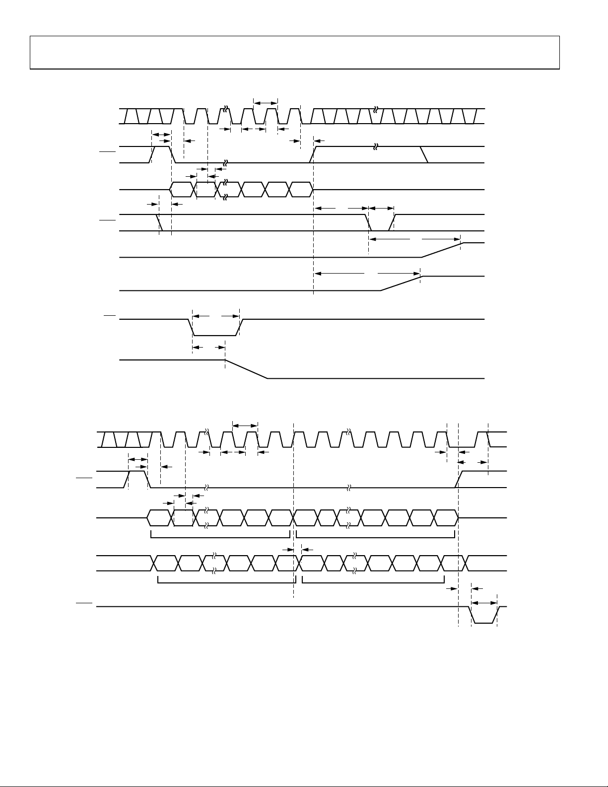
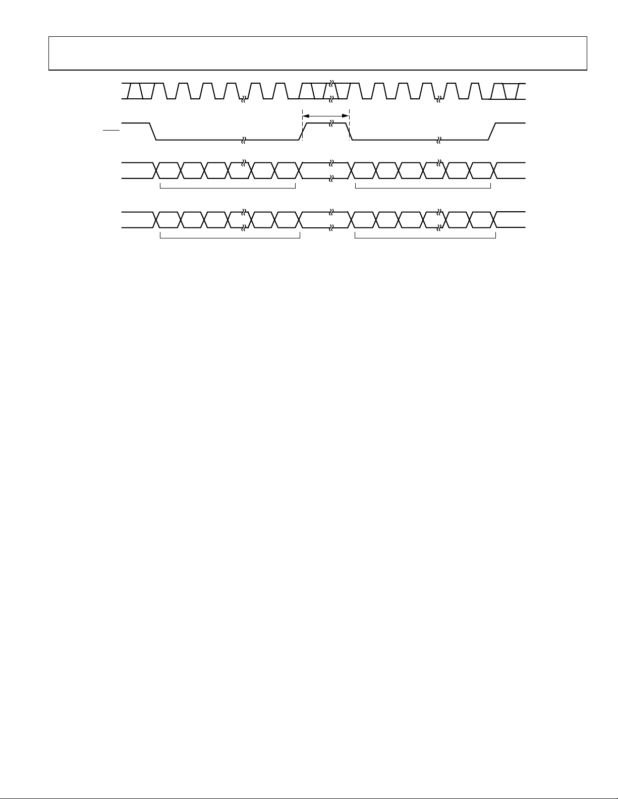
See Figure 2, Figure 3, and Figure 4.
4
Daisy-chain and readback mode.
5
C
= capacitive load on SDO output.
L SDO
MIN
to T
, unless otherwise noted.
MAX
Limit at t
, t
Unit Description
MIN
MAX
falling edge to SCLK falling edge setup time
SYNC
SCLK falling edge to SYNC
Minimum SYNC
falling edge to SYNC falling edge
LDAC
rising edge to LDAC falling edge
SYNC
pulse width low
LDAC
pulse width low
CLR
pulse activation time
CLR
rising edge to SCLK rising edge
SYNC
Minimum SYNC
Rev. A | Page 5 of 32
rising edge
high time (write mode)
5
= 15 pF)
L SDO
high time (readback/daisy-chain mode)
= 2 kΩ; C
LOAD
= 200 pF;
LOAD
AD5724/AD5734/AD5754
TIMING DIAGRAMS
t
1
SCLK
SYNC
SDIN
LDAC
V
OUT
V
OUT
V
OUT
CLR
t
6
t
4
t
7
DB23
t
9
x
x
x
t
3
t
8
t
13
t
14
4221
t
2
t
5
DB0
t
t
10
11
t
12
t
12
06468-002
Figure 2. Serial Interface Timing Diagram
t
1
SCLK
SYNC
SDIN
SDO
LDAC
8442
t
17
t
4
t
7
t
3
t
8
t
2
INPUT WO RD FOR DAC N – 1INPUT WO RD F OR DAC N
t
16
DB23
INPUT WO RD FOR DAC NUNDEFINED
t
5
t
15
D0BD32BD0BD32B
DB0
t
10
t
11
06468-003
Figure 3. Daisy-Chain Timing Diagram
Rev. A | Page 6 of 32
AD5724/AD5734/AD5754
SCLK
SYNC
1
24 24
t
1
17
SDIN
SDO
DB23 DB0 DB23 DB0
REGISTE R T O BE READ
DB23 DB0 DB23 DB0
UNDEFINED
NOP CONDITIONINPUT WORD SPECIFIES
SELECTED REGISTER DAT A
CLOCKED OUT
Figure 4. Readback Timing Diagram
06468-004
Rev. A | Page 7 of 32
AD5724/AD5734/AD5754
ABSOLUTE MAXIMUM RATINGS
TA = 25°C, unless otherwise noted.
Transient currents of up to 100 mA do not cause SCR latch-up.
Table 4. Stresses above those listed under Absolute Maximum Ratings
Parameter Rating
AVDD to GND −0.3 V to +17 V
AVSS to GND +0.3 V to −17 V
DVCC to GND −0.3 V to +7 V
Digital Inputs to GND
Digital Outputs to GND
REFIN to GND −0.3 V to +5 V
V
A, V
B, V
C, V
OUT
OUT
OUT
DAC_GND to GND −0.3 V to +0.3 V
SIG_GND to GND −0.3 V to +0.3 V
Operating Temperature Range, TA
Industrial −40°C to +85°C
Storage Temperature Range −65°C to +150°C
Junction Temperature, TJ max 150°C
24-Lead TSSOP Package
θJA Thermal Impedance 42°C/W
θJC Thermal Impedance 9°C/W
Power Dissipation (TJ max − TA)/ θJA
Lead Temperature JEDEC industry standard
Soldering J-STD-020
ESD (Human Body Model) 3.5 kV
D to GND AVSS to AVDD
OUT
−0.3 V to DV
(whichever is less)
−0.3 V to DV
(whichever is less)
+ 0.3 V or 7 V
CC
+ 0.3 V or 7 V
CC
may cause permanent damage to the device. This is a stress
rating only; functional operation of the device at these or any
other conditions above those indicated in the operational
section of this specification is not implied. Exposure to absolute
maximum rating conditions for extended periods may affect
device reliability.
ESD CAUTION
Rev. A | Page 8 of 32
AD5724/AD5734/AD5754
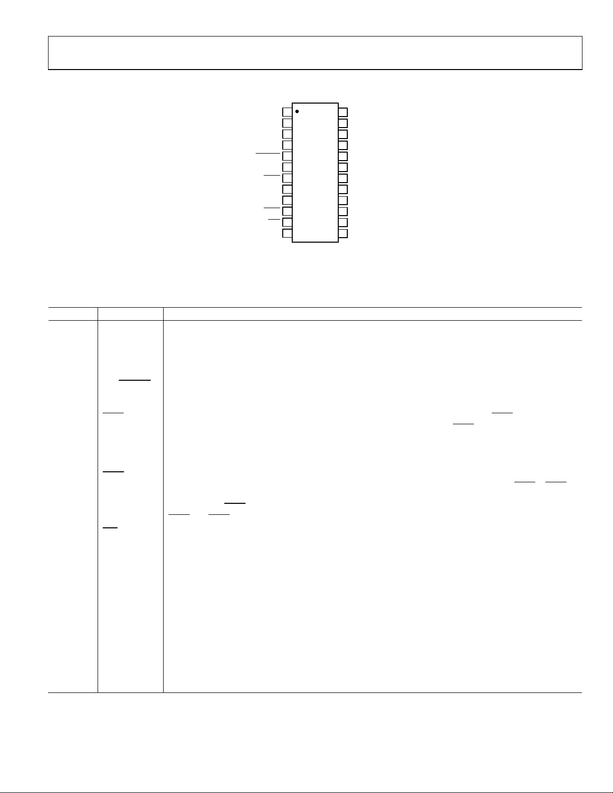
PIN CONFIGURATION AND FUNCTION DESCRIPTIONS
AV
1
AV
SS
2
NC
AD5724/
3
A
V
OUT
V
OUT
BIN/2sCOMP
SYNC
SCLK
SDIN
LDAC
CLR
NOTES
1. NC = NO CO NNECT.
2. IT IS RECOMMENDE D THAT THE EX POSED PAD BE
THERMALLY CONNECTED TO A COPPER PLANE
FOR ENHANCED THERM AL PERFORMANCE.
B
NC
NC
AD5734/
4
AD5754
5
TOP VIEW
6
(Not to S cale)
7
8
9
10
11
12
Figure 5. Pin Configuration
Table 5. Pin Function Descriptions
Pin No. Mnemonic Description
1 AVSS
Negative Analog Supply. Voltage ranges from −4.5 V to −16.5 V. This pin can be connected to 0 V if output
ranges are unipolar.
2, 6, 12, 13 NC Do not connect to these pins.
3 V
4 V
5
A Analog Output Voltage of DAC A. The output amplifier is capable of directly driving a 2 kΩ, 4000 pF load.
OUT
B Analog Output Voltage of DAC B. The output amplifier is capable of directly driving a 2 kΩ, 4000 pF load.
OUT
BIN/2sCOMP
Determines the DAC coding for a bipolar output range. This pin should be hardwired to either DVCC or GND.
When hardwired to DV
, input coding is offset binary. When hardwired to GND, input coding is twos
CC
complement. (For unipolar output ranges, coding is always straight binary).
7
Active Low Input. This is the frame synchronization signal for the serial interface. While SYNC is low, data is
SYNC
transferred on the falling edge of SCLK. Data is latched on the rising edge of SYNC.
8 SCLK
Serial Clock Input. Data is clocked into the shift register on the falling edge of SCLK. This operates at clock
speeds up to 30 MHz.
9 SDIN Serial Data Input. Data must be valid on the falling edge of SCLK.
10
Load DAC, Logic Input. This is used to update the DAC registers and consequently, the analog outputs. When
LDAC
this pin is tied permanently low, the addressed DAC register is updated on the rising edge of SYNC
held high during the write cycle, the DAC input register is updated, but the output update is held off until the
11
CLR
falling edge of LDAC
LDAC
. The LDAC pin should not be left unconnected.
Active Low Input. Asserting this pin sets the DAC registers to zero-scale code or midscale code (user-selectable).
. In this mode, all analog outputs can be updated simultaneously on the falling edge of
14 DVCC Digital Supply. Voltage ranges from 2.7 V to 5.5 V.
15 GND Ground Reference.
16 SDO
Serial Data Output. Used to clock data from the serial register in daisy-chain or readback mode. Data is
clocked out on the rising edge of SCLK and is valid on the falling edge of SCLK.
17 REFIN External Reference Voltage Input. Reference input range is 2 V to 3 V. REFIN = 2.5 V for specified performance.
18, 19 DAC_GND Ground Reference for the Four Digital-to-Analog Converters.
20, 21 SIG_GND Ground Reference for the Four Output Amplifiers.
22 V
23 V
D Analog Output Voltage of DAC D. The output amplifier is capable of directly driving a 2 kΩ, 4000 pF load.
OUT
C Analog Output Voltage of DAC C. The output amplifier is capable of directly driving a 2 kΩ, 4000 pF load.
OUT
24 AVDD Positive Analog Supply. Voltage ranges from 4.5 V to 16.5 V.
AV
Exposed
Paddle
SS
This exposed paddle should be connected to the potential of the AV
unconnected. It is recommended that the paddle be thermally connected to a copper plane for enhanced thermal
performance.
24
23
V
22
V
21
SIG_GND
20
SIG_GND
19
DAC_GND
18
DAC_GND
17
REFIN
16
SDO
15
GND
DV
14
NC
13
OUT
OUT
DD
C
D
CC
06468-005
. If LDAC is
pin, or alternatively, it can be left electrically
SS
Rev. A | Page 9 of 32
AD5724/AD5734/AD5754
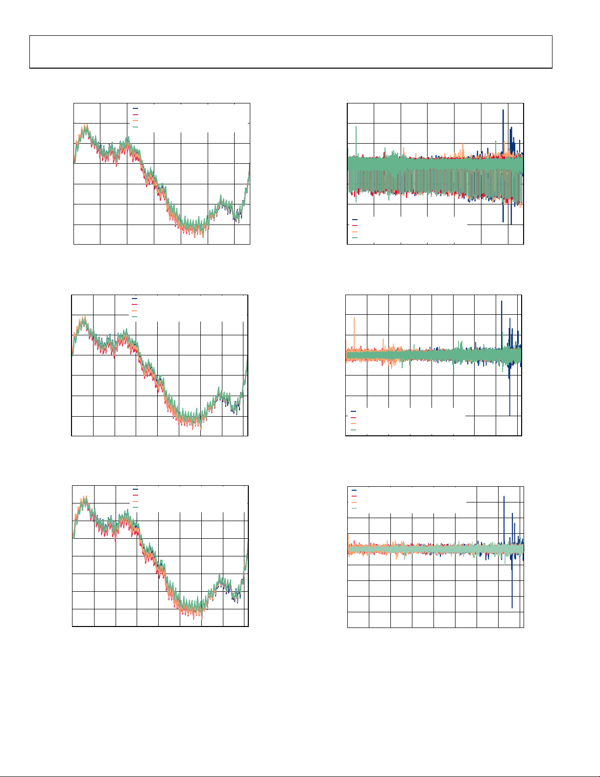
TYPICAL PERFORMANCE CHARACTERISTICS
6
4
2
AVDD/AVSS = +12V/0V, RANGE = +10V
AV
/AVSS = ±12V, RANGE = ±10V
DD
AV
/AVSS = ±6.5V, RANGE = ±5V
DD
AV
/AVSS = +6.5V/0V, RANGE = +5V
DD
0.6
0.4
0.2
0
–2
INL ERROR (LSB)
–4
–6
–8
0 10,000 20,000 30,000 40,000 50,000 60,000
CODE
06468-013
0
–0.2
DNL ERROR (LSB)
–0.4
AVDD/AVSS = +12V/0V, RANGE = +10V
–0.6
AV
/AVSS = ±12V, RANGE = ±10 V
DD
AV
/AVSS = ±6.5V, RANGE = ±5V
DD
AV
/AVSS = +6.5V/0V, RANGE = +5V
–0.8
DD
0 10,000 20,000 30,000 40000 50,000 60,000
CODE
Figure 6. AD5754 Integral Nonlinearity Error vs. Code Figure 9. AD5754 Differential Nonlinearity Error vs. Code
1.5
1.0
0.5
0
–0.5
INL ERROR (LSB)
–1.0
–1.5
–2.0
0 2000 4000 6000 8000 10,000 12,000 14,000 16,000
AVDD/AVSS = +12V/0V, RANGE = +10V
AV
/AVSS = ±12V, RANGE = ±10V
DD
AV
/AVSS = ±6.5V, RANGE = ±5V
DD
AV
/AVSS = +6.5V/0V, RANGE = +5V
DD
CODE
Figure 7. AD5734 Integral Nonlinearity Error vs. Code
6468-014
0.15
0.10
0.05
0
–0.05
DNL ERROR (LSB)
–0.10
–0.15
–0.20
AVDD/AVSS = +12V/0V, RANGE = +10V
AV
/AVSS = ±12V, RANGE = ±10V
DD
AV
/AVSS = ±6.5V, RANGE = ±5V
DD
AV
/AVSS = +6.5V/0V, RANGE = +5V
DD
0 2000 4000 6000 8000 10000 12000 14000 16000
CODE
Figure 10. AD5734 Differential Nonlinearity Error vs. Code
06468-016
06468-017
0.3
0.2
0.1
0
–0.1
–0.2
INL ERROR (LSB)
–0.3
–0.4
–0.5
0 500 1000 1500 2000 2500 3000 3500 4000
AVDD/AVSS = +12V/0V, RANGE = +10V
AV
/AVSS = ±12V, RANGE = ±10V
DD
AV
/AVSS = ±6.5V, RANGE = ±5V
DD
AV
/AVSS = +6.5V/0V, RANGE = +5V
DD
CODE
Figure 8. AD5724 Integral Nonlinearity Error vs. Code
06468-015
0.04
AVDD/AVSS = +12V/0V, RANGE = +10V
AV
/AVSS = ±12V, RANGE = ±10V
DD
AV
/AVSS = ±6.5V, RANGE = ±5V
DD
AV
/AVSS = +6.5V/0V, RANGE = +5V
DD
0
0 500 1000 1500 2000 2500 3000 3500 4000
CODE
DNL ERROR (LSB )
0.03
0.02
0.01
–0.01
–0.02
–0.03
–0.04
–0.05
Figure 11. AD5724 Differential Nonlinearity Error vs. Code
06468-018
Rev. A | Page 10 of 32
 Loading...