Industrial I/V Output Driver,
Single Supply, 60v Compliance,
Programmable Ranges
Preliminary Technical Data
FEATURES
Current Output Ranges: 4–20mA, 0–20mA or 0–24mA,
0.1% Total Unadjusted Error (TUE)
5ppm/°C Output Drift
60V MAX IOUT Compliance Voltage
Voltage Output Ranges: 0-5V, 0-10V, 0-40v
20% over-range
0.1% Total Unadjusted Error (TUE)
Flexible Serial Digital Interface
On-Chip Output Fault Detection
PEC Error Checking
Asynchronous CLEAR Function
Power Supply Range
AV
: = +12V to +60V (MAX)
DD
Output Loop Compliance to AV
Temperature Range: -40°C to +105°C
LFCSP Packages
APPLICATIONS
Process Control
Actuator Control
PLC
GENERAL DESCRIPTION
The AD5751 is a single channel, low-cost, precision,
voltage/current output driver with hardware or software
programmable output ranges. The software ranges are
configured via an SPI/Microwire compatible serial interface.
The AD5751 targets applications in PLC and industrial process
control. The analog input to the AD5751 is provided from a
low voltage, single supply digital-to-analog converter and is
internally conditioned to provide the desired output
current/voltage range.
The output current range is programmable across three current
ranges - 4–20mA, 0–20mA or 0–24mA.
– 2.5 V
DD
AD5751
Voltage output is provided from a separate pin that can be
configured to provide 0V to 5V, 0V to 10V and 0-40V output
ranges. An over-range of 10% is available on the voltage
ranges.
Analog outputs are short and open circuit protected and can
drive capacitive loads of 1uF and inductive loads of 0.1H.
The device is specified to operate with a power supply range
from 12 V to 60 V. Output loop compliance is 0 V to AV
2.5 V.
The flexible serial interface is SPI
and MICROWIRE
compatible and can be operated in 3-wire mode to minimize the
digital isolation required in isolated applications. The interface
also features an optional PEC error checking feature using
CRC-8 error checking, useful in industrial environments where
data communication corruption can occur.
The device also includes a power-on-reset function ensuring
that the device powers up in a known state and an
asynchronous CLEAR pin which sets the outputs to zero-scale /
mid-scale voltage output or the low end of the selected current
range.
A HW SELECT pin is used to configure the part for hardware
or software mode on power up.
The total output error is typically ±0.1% in both current mode
and voltage mode.
Table 1. Related Devices
Part Number Description
AD5422
Single Channel, 16-Bit, Serial
Input Current Source and
Voltage Output DAC
DD
–
Rev. PrA
Information furnished by Analog Devices is believed to be accurate and reliable. However, no
responsibility is assumed by Analog Devices for its use, nor for any infringements of patents or other
rights of third parties that may result from its use. Specifications subject to change without notice. No
license is granted by implication or otherwise under any patent or patent rights of Analog Devices.
Trademarks and registered trademarks are the property of their respective owners.
One Technology Way, P.O. Box 9106, Norwood, MA 02062-9106, U.S.A.
Tel: 781.329.4700 www.analog.com
Fax: 781.461.3113 ©2008 Analog Devices, Inc. All rights reserved.

AD5751 Preliminary Technical Data
TABLE OF CONTENTS
Features .............................................................................................. 1
Applications ....................................................................................... 1
General Description ......................................................................... 1
Revision History ............................................................................... 2
Functional Block Diagram .............................................................. 3
Specifications ..................................................................................... 4
Timing Characteristics ................................................................ 6
Absolute Maximum Ratings ............................................................ 9
ESD Caution .................................................................................. 9
Pin Configuration and Function Descriptions ........................... 10
Typical Performance Characteristics ........................................... 12
Terminology ................................. Error! Bookmark not defined.
Theory of Operation ................... Error! Bookmark not defined.
CURRENT OUTPUT Architecture ......................................... 14
OUTEN ........................................................................................ 14
Software control:......................................................................... 15
HARDWARE CONTROL: ........................................................ 17
Features ............................................................................................ 19
output fault alert – SOFTWARE MODE ................................ 19
output fault alert – HARDWARE MODE ............................... 19
voltage output short circuit protection .................................... 19
Asynchronous Clear (CLEAR) ................................................. 19
External current setting resistor ............................................... 20
Applications Information .............................................................. 21
Transient voltage protection ..................................................... 21
Layout Guidelines....................................................................... 21
Galvanically Isolated Interface ................................................. 21
Microprocessor Interfacing ....................................................... 21
Outline Dimensions ....................................................................... 22
Ordering Guide .......................................................................... 22
REVISION HISTORY
PrA – Preliminary Version. May 6, 2008
Rev. PrA | Page 2 of 22

Preliminary Technical Data AD5751
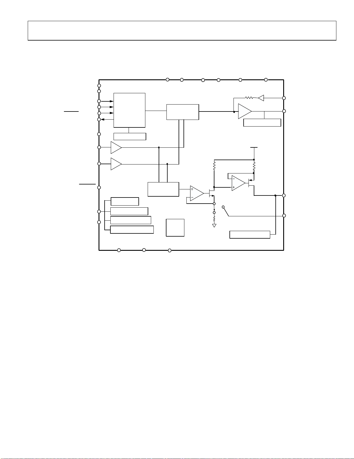
FUNCTIONAL BLOCK DIAGRAM
CLEAR
CLRSEL
SCLK/OUTEN*
SDIN/R0*
SYNC/RSEL*
SDO/VFAULT*
HW SELECT
VIN
VREF
RESET
FAULT/TEMP*
NC/IFAULT*
INPUT SHIFT
REGISTER
AND
CONTROL
LOGIC
STATUS REG
OVERTEMP
VOUT SHORT F A ULT
IOUT OPEN FAULT
OUTPUT RANG E ERROR
AD5751
DVCC
VOUT RANGE
SCALING
IOUT RANGE
SCALING
POWER
RESET
ON
GND
AVDD
GND
R2
R1
COMP2COMP1
VSENSE+
VOUT
VOUT SHORT FAULT
AVDD
R3
IOUT
RSET
IOUT OPEN FAULT
AD2/R1*
AD1/R2*
AD0/R3*
Figure 1. Functional Block Diagram
* Denotes shared pin. Software mode denoted by regular text, hardware mode denoted by bold
text. E.G. for FAULT/TEMP pin, in software mode this pin will take on FAULT function. In
Hardware mode, this pin will take on TEMP function.
Rev. PrA | Page 3 of 22

AD5751 Preliminary Technical Data
SPECIFICATIONS
AVDD=12V (+/-10%) to +60V (MAX) , DVCC =2.7 V to 5.5 V, GND = 0 V. RL = 2 kΩ, CL = 200 pF, IOUT : RL = 300Ω, HL =
50mH All specifications T
MIN
to T
Table 2.
Parameter Value
INPUT VOLTAGE RANGE
Input Leakage Current 1 uA max
VOLTAGE OUTPUT
Output Voltage Ranges 0 to 5 V
0 to 10 V
0 to 40 V
ACCURACY Output unloaded
Unipolar Output
Total Unadjusted Error (TUE) 0.1 % FSR max Over temperature and supplies.
Relative Accuracy (INL) ±0.02 % FSR max
Offset Error 0.015 % FSR max Error at analog input = 100mv (?)
Zero Scale Error TBD % FSR max Error at analog input = 0.0v
Zero Scale TC TBD ppm % FSR max
Gain Error 0.005 % FSR max (Ideal Span – Measured Span)/Ideal Span
Gain Error TC TBD ppm % FSR max
Full Scale Error 0.015 % FSR max Error at analog input = 4.096v (FS)
Full Scale Error TC TBD ppm % FSR max
Short-Circuit Current 15 mA max
Load Conditions
Resistance 1 K Ohm min For Specified Performance, 0-5v, 0-10v ranges.
Resistance 5 K Ohm min For Specified Performance, 0-40v ranges.
Capacitance Load Stability
RL = ∞ 20 nF max
RL = 2 kΩ TBD nF max
RL = ∞ 1 μF max External compensation capacitor of 4nF connected.
0.1% Settling Time
Slew Rate 1 V/μs typ
Output Noise TBD
Output Noise Spectral Density 100 nV/√Hz typ Measured at 10KHz
DC Output Impedance 0.3 Ω typ
DC PSRR 10 μV/V
AC PSRR TBD dB
Power-On Glitch Energy 10 nV-sec typ
CURRENT OUTPUT
Output Current Ranges 0 to 24 mA
0 to 20 mA
, unless otherwise noted.
MAX
1
Unit Test Conditions/Comments
0 to 4.096 V
AVDD needs to have minimum 1.1v headroom, or
>11.1v.
10 us Specified with 200pF load
μV rms max
80
μV rms max
Rev. PrA | Page 4 of 22
0.1 Hz to 10 Hz Bandwidth
100 kHz Bandwidth
200mV 50/60Hz Sinewavesuperimposed on power
supply voltage.

Preliminary Technical Data AD5751
Parameter Value1 Unit Test Conditions/Comments
4 to 20 mA
ACCURACY
Total Unadjusted Error (TUE) ±0.1 % FSR max With External Precision Resistor
TUE TC ±5 ppm max
Unipolar Output
Relative Accuracy (INL) ±0.02 % FSR max
Offset Error 0.01 % FSR max Error at analog input = 100mv (?)
Zero Scale Error 0.01 % FSR max Error at analog input = 0.0v
Zero Scale TC TBD ppm % FSR max
Gain Error 0.15 % FSR max (Ideal Span – Measured Span)/Ideal Span
Gain Error TC TBD ppm % FSR max
Full Scale Error 0.01 % FSR max Error at analog input = 4.096v (FS)
Full Scale Error TC TBD ppm % FSR max
Total Unadjusted Error (TUE) ±0.3 % FSR max With Internal Resistor
TUE TC ±20
±50
Unipolar Output
Relative Accuracy (INL) ±0.02 % FSR max
Offset Error 0.01 % FSR max Error at analog input = 100mv (?)
Zero Scale Error 0.01 % FSR max Error at analog input = 0.0v
Zero Scale TC TBD ppm % FSR max
Gain Error 0.15 % FSR max (Ideal Span – Measured Span)/Ideal Span
Gain Error TC TBD ppm % FSR max
Full Scale Error 0.01 % FSR max Error at analog input = 4.096v (FS)
Full Scale Error TC TBD ppm % FSR max
Output Current Ranges
(over range)
0.1 to 20.4 mA
3.9 to 20.4 mA
Relative Accuracy (INL) ±0.02 % FSR max
OUTPUT CHARACTERISTICS
Current Loop Compliance Voltage AVDD – 2.5 V max
Resistive Load See Comment kΩ max Chosen such that compliance is not exceeded.
Inductive Load 0.1 H max
0.1% Settling Time
DC PSRR 1 μA/V max
Output Impedance 25 MΩ typ
REFERENCE INPUT
Reference Input
Reference Input Voltage 4.096 V nom ±1% for specified performance
Input Leakage Current 1 uA max
DIGITAL INPUTS
VIH, Input High Voltage 2 V min
0.1 to 24.5 mA Nominal Over-ranges. See Text Page..
10 us
DVCC = 2.7 V to 5.5 V, JEDEC compliant
ppm typ
ppm max
Rev. PrA | Page 5 of 22
With External Precision Resistor
With Internal Resistor

AD5751 Preliminary Technical Data
Parameter Value1 Unit Test Conditions/Comments
VIL, Input Low Voltage 0.8 V max
Input Current ±1 μA max Per pin
Pin Capacitance 10 pF typ Per pin
DIGITAL OUTPUTS
FAULT, IFAULT, TEMP, VFAULT
VOL, Output Low Voltage 0.4 V max
VOL, Output Low Voltage 0.6 V typ @ 2.5 mA
VOH, Output High Voltage 3.6 V min
SDO
VOL, Output Low Voltage 0.5 V max Sinking 200ua
VOH, Output High Voltage DVCC-0.5 V min Sourcing 200ua
High Impedance Leakage
current
High Impedance Output
Capacitance
POWER REQUIREMENTS
AVDD 12 to 24 V min to V max +/-10%
DVCC
Input Voltage 2.7 to 5.5 V min to V max Internal supply disabled
AVDD TBD mA Output unloaded
DICC TBD mA max VIH = DVCC, VIL = GND, TBD mA typ
Power Dissipation TBD mW typ
1
Temperature range: -40°C to +105°C; typical at +25°C.
10kΩ pull-up resistor to DV
10kΩ pull-up resistor to DV
±TBD ua max
20 pF max
CC
CC
TIMING CHARACTERISTICS
AVDD=12V (+/-10%) to +60V (MAX) , DVCC =2.7 V to 5.5 V, GND = 0 V. RL = 2 kΩ, CL = 200 pF, IOUT : RL = 300Ω, HL =
50mH All specifications T
Table 3.
Parameter
1, 2
Limit at T
t1 33 ns min SCLK cycle time
t2 13 ns min SCLK high time
t3 13 ns min SCLK low time
t4 13 ns min
t5 13 ns min
t6 100 ns min
t7 5 ns min Data setup time
MIN
to T
, unless otherwise noted.
MAX
, T
MIN
Unit Description
MAX
falling edge to SCLK falling edge setup time
SYNC
th
SCLK falling edge to SYNC rising edge
16
Minimum SYNC
Rev. PrA | Page 6 of 22
high time (WRITE MODE)

Preliminary Technical Data AD5751
V
T
t8 0 ns min Data hold time
t10 , t9 1 μs max CLEAR pulse high/low activation time
t11 200 ns min
t
25 ns max SCLK rising edge to SDO valid (SDO CL=20pf)
12
t
1 us max CLEAR pulse low activation time
13
1 Guaranteed by characterization. Not production tested.
2 All input signals are specified with t
= tF = 5 ns (10% to 90% of DVCC) and timed from a voltage level of 1.2 V.
R
Minimum SYNC
high time (READ MODE)
O OUTPUT
PIN
C
15pF
200µA I
L
200µA I
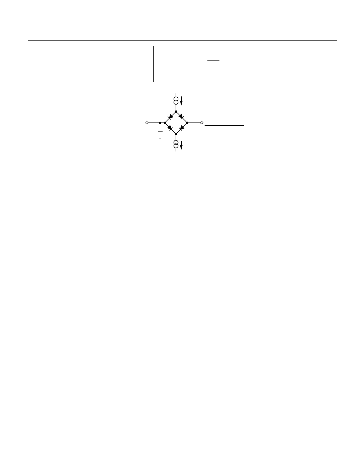
SDO Load Timing.
OL
OH(min)-VOL(max)
2
OH
Rev. PrA | Page 7 of 22
 Loading...