

GSM
ALGORITHM
SIGNAL
PROCESSOR
ASP
PHYSICAL
LAYER
PROCESSOR
PLP
µC
BASEBAND
CONVERTER
BBC
RADIO
SUBSYSTEM
512K x 16
ROM
128K x 8
RAM
DISPLAY
2K x 8
EEPROM
KEYPAD SIM
AD20msp410
GSM CHIPSET
a
FEATURES
Passed European GSM Phase I Type Approval
Complete Baseband Processing Chipset Performs:
Speech Coding/Decoding, According to GSM 06.XX
DTMF and Call Progress Tone Generation
Equalization with 16-State Viterbi, Soft Decision
Channel Coding/Decoding According to GSM 05.03
All ADC and DAC Interface Functions
Includes all Radio, Auxiliary and Voice Interfaces
Support for GSM Data Services
Embedded 16-Bit Microcontroller
Layer 1 Software Provided with Chipset
Full Phase 2 Protocol Stack Software Available
Integrated SIM- and Keyboard Interface
Ultralow Power Design
2.7 V Operating Voltage
Intelligent Power Management Features
Up to 70 Hours Standby Time Achievable
JTAG-Boundary Scan
Full Reference Design Available
Three TQFP Devices, Occupying Less than 12 cm
APPLICATIONS
GSM/DCS1800 Mobile Radios and PCMCIA Cards
Baseband Processing Chipset
AD20msp410
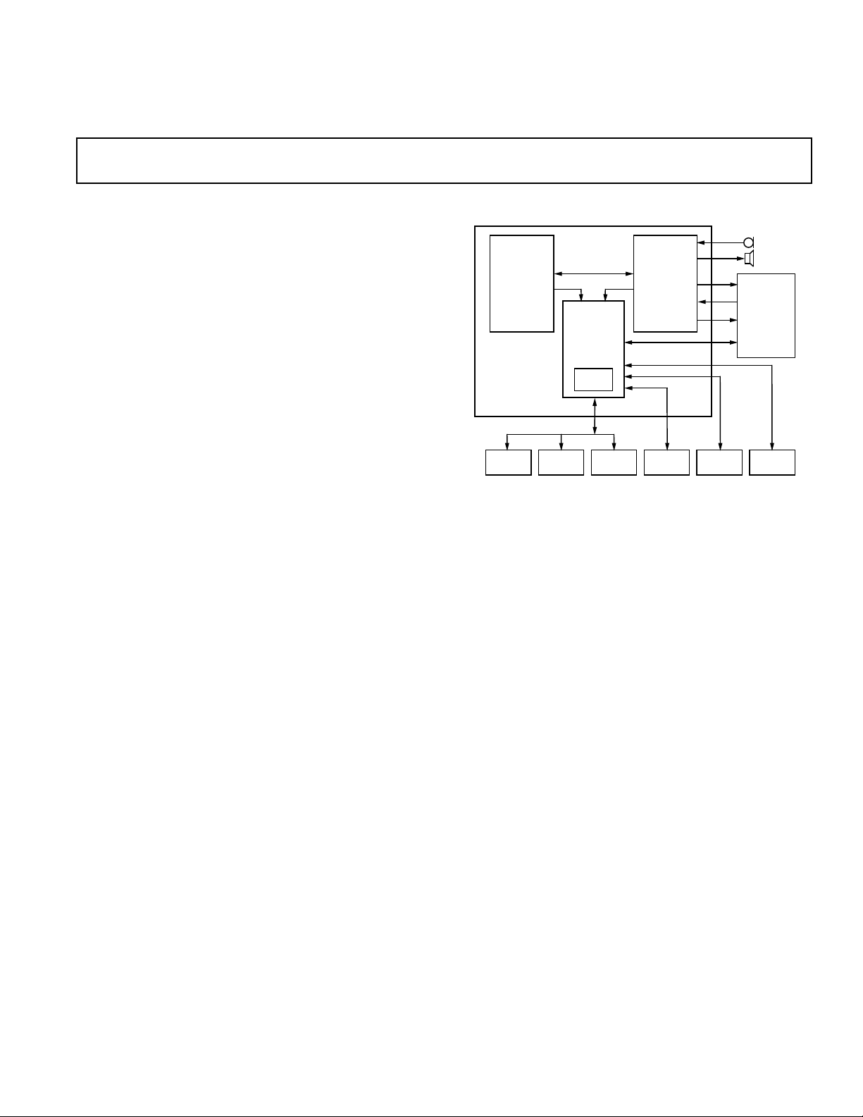
SYSTEM ARCHITECTURE
2
GENERAL DESCRIPTION
The Analog Devices GSM baseband processing chipset provides
a competitive solution for GSM based mobile radio systems. It
is designed to be fully integrated, easy to use, and compatible
with a wide range of product solutions. GSM phones using this
chipset and its accompanying Layer 1, 2, 3 software have passed
the European GSM full type approval process.
The chipset consists of three highly integrated, sub-micron, low
power CMOS components that form the core baseband signal
processing of the GSM handset. The system architecture is
designed to be easily integrated into current designs and form
the basis of next generation of designs.
The chipset uses an operating voltage of 2.7V to 3.6 V, which
coupled with the extensive power management features,
significantly reduces the drain on battery power and extends the
handset’s talktime and standby time.
CHIPSET COMPONENTS
Algorithm Signal Processor (ASP)
The ASP is an application specific variant of the ADSP-2171
standard DSP from Analog Devices. It has been optimized to
meet the cost, size and power consumption requirements of
GSM mobile applications. All necessary memory to run the
GSM specific programs is provided on-chip and with its
REV. 0
Information furnished by Analog Devices is believed to be accurate and
reliable. However, no responsibility is assumed by Analog Devices for its
use, nor for any infringements of patents or other rights of third parties
which may result from its use. No license is granted by implication or
otherwise under any patent or patent rights of Analog Devices.
preprogrammed ROM, no user programming is required. The
ASP implements full rate speech transcoding according to GSM
specifications, including Discontinuous Transmission (DTX)
and Comfort Noise Insertion (CNI). A high performance softdecision Viterbi equalizer is also implemented in software,
embedded in the ROM.
Physical Layer Processor (PLP)
The PLP combines application specific hardware and an
embedded 16-bit microcontroller (Hitachi H8/300H) to
perform channel coding and decoding and execute the protocol
stack and user software. The embedded processor executes the
Layer 1, 2, 3 and user MMI software. The PLP can control all
powerdown functions of the other chips and memory support
components to achieve maximum power savings.
Baseband Converter (BBC)
The BBC performs the voiceband and baseband analog-todigital and digital-to-analog conversions, interfacing the digital
sections of the chipset to the microphone, loudspeaker and radio
section. In addition, the BBC contains all the auxiliary converters for burst-ramping, AFC, AGC, battery and temperature
monitoring. The chipset interfaces directly with a variety of
industry standard radio architectures and supplies all the
synthesizer and timing control signals.
© Analog Devices, Inc., 1996
One Technology Way, P.O. Box 9106, Norwood, MA 02062-9106, U.S.A.
Tel: 617/329-4700 Fax: 617/326-8703
AD20msp410
Software
The required Layer 1 software is supplied with the chipset. In
addition, an object code license for Layers 2 and 3 of the
protocol stack is available. This exact package of Layers 1,2,3 of
software, coupled with the AD20msp410 chipset, is today in
phones that have passed European GSM Final Type Approval.
Architecture Overview
A standard GSM Handset can be divided into five functional
areas:
• Analog and Digital Baseband Processing Subsystem
• (Voice to Radio)
• Layer 1 Software (Physical Layer)
• Protocol Stack Software (Layers 2 and 3)
• Radio Subsystem
• User Interface Software (MMI)
Analog Devices and The Technology Partnership (TTP)
provide a cost effective and proven method of attaining the
baseband processing subsystem and protocol stack software.
This data sheet includes functional descriptions of the baseband
processing subsystem and the Layer 1 software. The Technology Partnership can provide licenses to software and reference
designs in all the other areas of a GSM hand-portable terminal.
For detailed information about the individual chipset components, please refer to the ADSP-2178 (ASP), AD7015 (BBC)
and ADPLP01 (PLP) data sheets for electrical characteristics
and timing information.
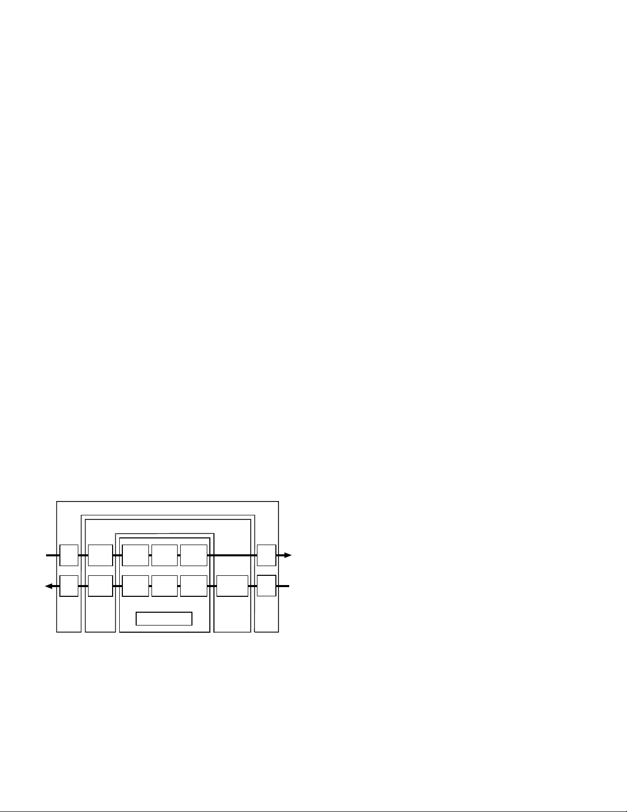
FUNCTIONAL DESCRIPTION
Figure 1 is a functional block diagram of the GSM baseband
processing chipset. The chipset can be viewed as a functional
block that contains a number of discrete functional units. The
electrical and functional interfaces to the rest of the system are
briefly described at the end of this section and described in
detail in the individual data sheets for each component.
BBC
ASP
VOICE
ADC
VOICE
DAC
SPEECH
ENCODE
SPEECH
SPEECH
DECODE
ENCODE
CHANNEL
ENCODE
CHANNEL
DEINTER-
DECODE
CONTROL + MMI + I/O
INTERLEAVE
LEAVE
PLP
ENCRYPT
DECRYPT
EQUALIZER
BASEBAND
DAC
BASEBAND
ADC
Figure 1. Functional Description
UPLINK
The uplink baseband processing functions include the following
operations:
Analog-to-Digital Voice Conversion (BBC)
A conventional microphone, connected directly to the BBC,
provides an analog input signal to the ADC. The voice ADC
function uses a sigma-delta converter to convert and noise shape
the input signal, achieving a Signal-to-Noise Ratio plus Total
Harmonic Distortion (SNR+THD) of greater than 62.5 dB.
–2–
The analog voice signal is sampled at 8 kHz, producing 13-bit
linear values corresponding to the magnitude of the input. The
resulting data is passed to the ASP through a dedicated serial
port.
Speech Encoding (ASP)
The ASP receives the voice data stream from the BBC and
encodes the data from 104 kb/s to 13 kb/s. The algorithm used
is Regular Pulse Excitation, with Long Term Prediction (RPELTP) as specified in the 06-series of GSM recommendations.
The algorithm is tested and proven to be bit-exact against the
GSM test vectors including all VAD/DTX functions. After
encoding the data is transferred to the PLP through a parallel
port in discrete blocks of 260 bits at 20 ms intervals.
Channel Coding (PLP)
The information received from the ASP contains data values
and filter coefficients that have different levels of priority. These
are subsequently protected to different levels within the channel
coding. The encode protection process incorporates block
coding and convolutional encoding. In addition to the normal
speech traffic channels, the channel coding function also
supports data transmission at full rate and half rate. After the
interleave process, if necessary, the data is encrypted using the
required A5/1 or A5/2 encryption algorithm. Data is then
formatted into bursts, with the required timing and training
sequences and sent to the BBC through a dedicated serial port.
GMSK Modulation and D/A Conversion (BBC)
The BBC receives data at 270 kb/s. The on-chip lookup-table
ROM modulates and spectrally shapes the data being sent. A
pair of 10-bit matched differential DACs convert the modulated
data from the digital domain to the analog domain and pass I
and Q data to the transmit section of the radio subsystem.
DOWNLINK
The downlink baseband processing functions include the
following operations:
Analog-to-Digital Conversion (BBC)
The receiver I and Q signals are sampled by a pair of ADCs at
270 kHz. The resulting digital words are transferred to the ASP
through a dedicated receive path serial link and DMA control.
Equalization (ASP)
The equalizer recovers and demodulates the received signal and
establishes local timing and frequency references for the mobile
unit. The equalization algorithm is a version of the Maximum
Likelihood Sequence Estimation (MLSE) using the Viterbi
algorithm. Two confidence bits per symbol provide additional
information about the accuracy of each decision to the channel
codec’s convolutional decoder. The equalizer outputs a
sequence of bits including the confidence bits. This data is
transferred to the PLP through a dedicated parallel port on the
ASP. At this point, the training sequence and trailing bits,
contained within the burst, are discarded.
Channel Decoding (PLP)
The A5/1 or A5/2 decryption algorithm is used, as required, to
recover the data that is ready for the deinterleave process. The
deinterleave process is an exact inversion of the interleave
process used by the transmit section. Data can pass directly to
this function, without the A5/1 or the A5/2 decryption, controlled by the Layer 1 processing. The decode function then
performs convolutional decoding and parity decoding. The
convolutional decoder uses a Viterbi algorithm, with two soft
REV. 0
AD20msp410
decision confidence bits supplied by the equalizer. Once these
decoding functions are complete, digitized voice data is transferred to the ASP through a parallel port. Error control mechanisms are used to ensure adequate bad frame indication.
Speech Decoding (ASP)
Encoded speech data is transferred at 20 ms intervals from the
PLP to the ASP in blocks of 260 bits plus the Bad Frame
Indicator (BFI). The speech decoder supports a Comfort Noise
Insertion (CNI) function that inserts a predefined silence
descriptor into the decoding process. The ASP also implements
control of talker side-tone and short term echo cancellation.
The resulting data, at 104 kb/s, is transferred to the BBC
through a dedicated serial path.
Voice Digital-to-Analog Conversion
The Voice DAC function of the BBC uses a sigma-delta converter to convert and noise shape the signal. The 13-bit linear
values are converted to the analog domain and filtered to avoid
any images. The resulting differential signals can be controlled
in volume and drive directly a small earpiece as well as a
separate auxiliary output.
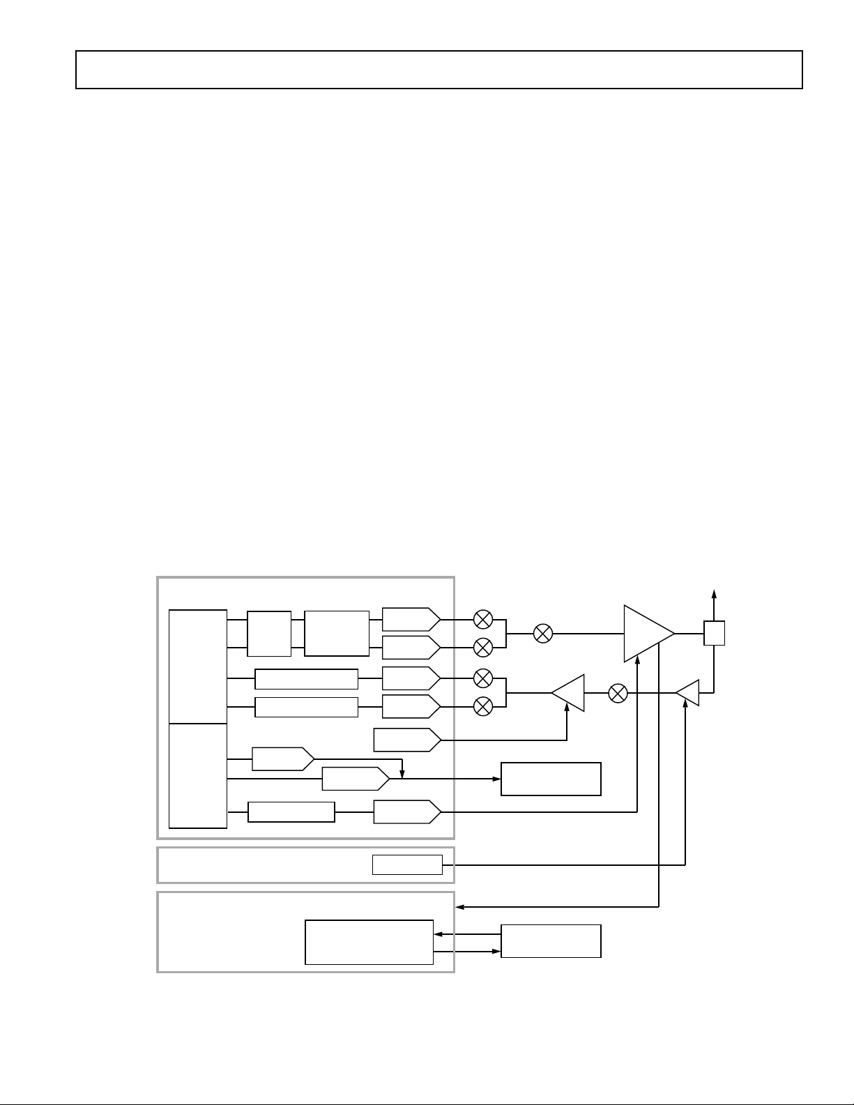
AUXILIARY SYSTEM FUNCTIONS
The ASP, the PLP and the BBC perform a number of auxiliary
functions which are essential to build a complete mobile radio.
A general radio section constitutes the three functions of
transmitter, receiver and synthesizer. Figure 2 shows how the
baseband chipset interfaces to a typical radio architecture. The
transmitter is fed with baseband analog I and Q signals from the
BBC and upconverted to 900 MHz for GSM applications and
1800 MHz for PCN applications.
A dedicated power amplifier increases the RF-signal to the
required level. The receiver amplifies the antenna signal, downconverts it to an intermediate frequency (IF) and amplifies it
there again. After second conversion to baseband, the I and Q
components of the signal are fed into the BBC.
The BBC, ASP and PLP provide three auxiliary functions for
interfacing to the radio subsystem. These auxiliary functions
include AGC, AFC and Power Ramping.
Power Ramp Envelope (BBC)
To meet the spectral and time-domain specifications of the
transmitted output signal, the burst has to follow a specified
power envelope. The envelope for the power profile originates in
the PLP as a set of coefficients, down-loaded and stored in the
BBC. This envelope profile is sent to one of the auxiliary DACs
on the BBC with each burst. The analog output is fed into the
RF power amplifier, controlling the power profile and absolute
level of the transmitted data.
Automatic Gain Control (AGC)
The mobile radio has to cope with a wide range of input signal
levels. The major part of the overall gain is provided in the IF
amplifier. The incoming signal level is analyzed in the ASP and
the PLP and a digital gain control signal is sent to the BBC. A
10-bit auxiliary DAC generates the appropriate analog control
signal for the IF amplifier. Additionally gain control can be
implemented by using two output flags of the ASP.
BASEBAND/AUXILIARY SECTION OF AD7015
TX DAC
TX DAC
RX DAC
RX DAC
10-BIT DAC
10-BIT DAC
FLAGS
BASEBAND
SERIAL
INTERFACE
AUXILIARY
SERIAL
INTERFACE
BURST
STORE
DIGITAL FIR FILTER
DIGITAL FIR FILTER
DIGITAL FIR FILTER
DIGITAL FIR FILTER
DIGITAL FIR FILTER
8-BIT DAC
RAMPING RAM
MODULATOR
ASP
GSMSK
10-BIT DAC
PLP
SYNTHESIZER
CONTROL SIGNALS
I
Q
I
Q
AFC
LOCK
PA
IF
AGC
13 MHz VCTCXO
RAMP CONTROL
AGC
PAERROR
13 MHz VCTCXO
REV. 0
Figure 2. Control of RF Section
–3–

AD20msp410
V110'
FRAMES
MAN MACHINE INTERFSCE
DATA APPLICATION
LAYER 2 RELAY (L2R)
RADIO LINK PROTOCOL (RLP)
RATE ADAPTION
EXTERNAL
DATA TERMINAL
ADAPTER
HANDSET
APPLICATION LAYER
FOREGROUND
COMMAND
INTERPRETER
FRAME
ROUTER
DATA TERMINAL
ADAPTER
APPLICATION LAYER
BACKGROUND
PROTOCOL STACK
LAYERS 2/3
PROTOCOL STACK
LAYER 1
AD20msp410
CHIPSET
Automatic Frequency Control (AFC)
The mobile radio has to track precisely the master clock
provided by the base station. Drift of the crystal oscillator over
time and temperature has to be compensated as well as frequency shifts due to the Doppler effect in the case of a moving
mobile radio. The received signal is analyzed in the ASP and the
PLP and a digital control signal is generated. This signal is sent
to the two DACs in the BBC. The 10-bit DAC operates as
coarse and the 8-bit DAC as fine adjust. The weighting of the
DACs is such, that both DACs yield a combined resolution of
13 bits. The combined analog output signal is used to control
the voltage controlled, temperature compensated crystal
oscillator (VCTCXO).
Synthesizer Control
The PLP and the respective parts of the Layer 1 software
control the overall timing and frequency generation of the radio
subsystem. This includes control signals for up to two synthesizers, powerdown control signals and power amplifier monitor
signals. Detailed information can be found in the ADPLP01
data sheet.
Generation of Auxiliary Audio Signals
Under control of Layer 1 the ASP can generate a variety of fixed
and user-programmable tones. This includes all standard
DTMF and Call Progress tones as well as user defined tones.
The tone structure can consist of up to four frequency components with individual durations.
The ASP also generates Talker Sidetone as specified in the
GSM recommendations. In comparison to traditional hardware
implementations, this software implementation provides manufacturing flexibility over a wide range of speaker/microphone
sensitivities.
AUDIO/AUXILIARY SECTION
VOICEBAND
INTERFACE
AUXILIARY
INTERFACE
Figure 3 shows the audio section and the auxiliary ADC of the
BBC. Input signals can come from either a directly connected
microphone or from a remote microphone in a car kit. Input
gain can be set to 0 dB or +26 dB. The output signal can be
directly connected to a small earpiece and, for further amplification, to an external car-kit. Two output-PGAs can be programmed for –15 dB or +6 dB.
VOLTAGE
REFERENCE
MUX
PGA
PGA
MUX
SERIAL
SERIAL
FILTER Σ/∆ DAC PGA
Σ/∆ DAC
FILTER
10-BIT DAC
Figure 3. Audio-/Auxiliary Section of AD7015
LOCK
CAR
KIT
U
BAT
TEMP
OTHER
DATA SERVICES
Data Services is considered to be an essential feature for GSM
terminals and the AD20msp410 chipset is designed to provide
flexible and low cost implementation of Data Services supported
via the GSM air interface.
Figure 4. Implementation of Data Services
The selected system architecture shown in Figure 4 provides for
minimum terminal Bill of Materials, the lowest possible number
of interconnection points and the lowest power consumption
when running speech traffic only. However, the chipset provides
full channel coding and decoding for all Data Services. Parity
and convolutional encoding and interleaving for TCH/F9.6,
TCH/F4.8 and TCH/F2.4 are implemented in the PLP.
The interface to the chipset is a user-configurable, 3-wire serial
interface supplying V110 data packets as defined in GSM 05.03,
combined with protocol information and control to the Application Layer. External to the terminal is the Data Terminal
Adapter (DTA) which runs the Data Services Software. Included
in the DTA are the rate adaptation functions and the Data
Services application. The Command Interpreter resident on the
mobile supports a serial interface protocol with the DTA via
both traffic data and control information are communicated.
The Technology Partnership can provide all requisite Data
Services Software.
SOFTWARE IMPLEMENTATIONS
A full implementation of the GSM Layer 1 functionality is
supplied as an object code module, for execution on the
controller, embedded in the PLP. Functions performed by this
software include:
• Initial scan of GSM band and selection of strongest thirty
channels as required by 03.22 and 05.08
• Mobile oscillator adjustment, timing synchronization and
BCCH decoding from serving cell (camping-on)
• Base station frequency and timing measurements and BSIC
extraction from neighbor cells under control of Layer 3
• Frequency hopping according to 05.02
• Full implementation of discontinuous reception (DRX) and
transmission (DTX)
• Reporting of received level and signal quality
–4–
REV. 0

AD20msp410
• Full engineering and test mode support
• Support for all phase 1 and phase 2 handover modes
• SIM Interface driver
• Message interfacing to Layer 3 (Radio Resources Manager)
and Layer 2 (data link layer, both signaling and data)
• External functions for AGC, AFC and synthesizer setting are
called by Layer 1. These allow the user to configure the
system for a wide range of radio architectures including the
TTP GSM reference radio.
• The higher layers of the protocol stack also reside on this
embedded processor. A GSM Phase 2 compliant, Layer 2/3
protocol stack is available from The Technology Partnership.
POWER DISSIPATION CONSIDERATIONS
In mobile applications, minimizing the power consumption of
all devices is critical to achieving longer standby and talk times.
In a GSM handset the baseband subsystem dominates the
current consumption of the phone in standby. The design of the
ASP, PLP and BBC includes extensive features to reduce current
consumption and give standby times of up to 70 hours.
All three devices were specifically designed to operate from
2.7 V to 3.6 V, so facilitating three or four cell NiCad/NiMH or
single-cell Li Ion batteries.
The PLP incorporates intelligent power management, permit-
ting automatic control of power consumption in the PLP and
the peripheral circuitry. Data processing modules are switched
on only when they process data, otherwise they are powered
down.
Additional control signals are provided that enable the Layer 1
software to control the external subsystems, such as the ASP,
BBC, radio and memory components, so that their power is
intelligently switched by the PLP.
Within the ASP the different powerdown modes range from a
simple “wait for interrupt” state to a complete hardware
powerdown, with only leakage currents dissipating power.
In the BBC, the powerdown functions are split separately
between receive, transmit and auxiliary circuits. This provides
optimal analog power performance when operating in different
modes.
INTERFACES
Figure 5 shows the chipset’s eight interfaces, which have to be
considered in the design of the complete mobile radio. Some of
these interfaces have to meet GSM specifications, others will be
design specific.
• Analog Voice Interface to BBC
• Radio Interface to BBC and PLP
• Digital SIM Card Interface to PLP
• Digital Interface to the Keypad
• Digital Bus Interface from PLP to Memory and Display
• Digital Interface from the PLP to the EEPROM
• Digital Audio Interface (DAI)
• Digital Interface to PLP for Data Services
Analog Voice Interface to BBC
The analog voice interface to the BBC is specified in the
AD7015 data sheet. Several design examples are given for
single-ended or differential inputs or outputs. A voltage
reference for biasing the microphone signal is provided on the
BBC. The analog output of the BBC is capable of driving an
earpiece directly with and impedance of 150 Ω. For optional
use of a separate external microphone and power amplifier, a set
of auxiliary inputs/outputs is provided.
Radio Interface to BBC and PLP
The analog interface between the BBC and the radio subsystem
consists of differential inputs and outputs for the I and Q parts
of the signal and three analog control signals for AFC, AGC and
transmit ramp envelope. Details of these signals are specified in
the AD7015 data sheet. The digital interface between the PLP
and the radio subsystem consists of a serial port for communicating with the synthesizers and several control signals as
specified in detail in the ADPLP01 data sheet.
Digital SIM Card Interface to PLP
The PLP is designed to interface directly to the SIM. However
interface logic may be necessary to connect the 3 V chipset to a
5 V SIM.
Digital Interface to Keypad
Keypad interface logic for up to 40 keys is provided on the PLP.
This interface provides keyboard scan for 8 Rows and 4
columns. Additionally an extra pin on the PLP is provided for
the power switch.
Digital Bus Interface to Memory and Display
External RAM and ROM as well as the display controller
interfaces directly to the 21-bit address bus and 16-bit data bus
of the PLP.
Interface to FLASH Memory
The large FLASH memory can contain all programs for the
embedded Control Processor of the PLP. This includes the
complete GSM protocol software as well as the User Interface
Software. A size of 4 Mbit to 8 Mbit is suggested to accommodate all Protocol software plus a typical size of User Interface
Software. Enhanced features, requiring larger memories are
supported easily by the large address space of the embedded
Control Processor. To facilitate production programming and
field upgrades of the FLASH memories, the PLP provides
embedded code to download the software into the FLASH
memory via its standard serial port.
Interface to SRAM
Beside the FLASH memory, the Control Processor additionally
supports static RAM to store user defined variables, typically
those used by the Protocol Stack or Application Layer. Standard
SRAMs interface directly to the address and data bus of the
PLP.
Interface to Display Controller
This interface is achieved through the address and data buses
and associated read and write strobes, as well as a specific
enable signal. An integrated wait state generator helps interface
to a wide range of display controllers. Two pins with PWM
outputs control the intensity of separate backlights for display
and keypad.
REV. 0
–5–

AD20msp410
Digital Audio Interface (DAI)
As required by the GSM specifications, a digital audio interface
is provided to allow certain tests of the audio section during type
approval. This interface is provided by the serial bus between
the ASP and the PLP and two additional control signals from
the PLP. A fully functional “DAI Box” needed for the FTA
process may be obtained from Analog Devices upon request.
Digital Interface to the PLP for Data Services
A conventional H8 serial port combined with a proprietary
protocol is used to interface to an external Data Terminal
Adapter.
Digital Interface from the PLP to the EEPROM
The PLP provides separate pins to interface directly to an
external EEPROM via a serial port. This EEPROM is typically
used for storage of calibration or user variable parameters like
handset identifier (IMEI), language, keypad lock and radio
calibration parameters. A typical size of the EEPROM is 2K × 8
bits, but this depends on the individual design of the handset.
GSM Baseband Processing Key Parts List
Table 1 lists the major hardware components necessary to
complete the GSM baseband processing subsystem. An example
Bill Of Material is available from Analog Devices. A full
reference design is available through Analog Devices/The
Technology Partnership.
Table I. List of Key Components
Quantity Description Specification
1 ASP
1 PLP
1 BBC
1 FLASH-PROM
1 SRAM 128K × 8, 120 ns
1 EEPROM
1
1
1
3
ADSP-2178
ADPLP01
AD7015
2
256K × 16, 150 ns
2K × 8
1 Display Driver Design Specific
NOTES
1
These components comprise the AD20msp410 chipset.
2
A size of 4 Mbits is recommended to allow storage of all GSM Layer
(1, 2, 3) programs as well as a typical user interface (MMI). Larger
memory can be used to support enhanced user interfaces.
3
Can be omitted if parameters are stored in FLASH memory.
SIM CARD
FLASH
MEMORY
SRAM
DISPLAY
CONTROLLER
KEYPAD
KEYPAD
DATA
INTERFACE
SIM BUFFER
SIM
INTERFACE
SERIAL PORT
ADDRESS
DATA
PSRAM
CONTROL
DISPLAY
CONTROL
BACKLIGHT
CONTROL
KEYPAD
INTERFACE
EEPROM
INTERFACE
DATA
INTERFACE
PLP
DAI CONTROL
SYNTHESIZER
ASP
INTERFACE
POWER
CONTROL
AND RADIO
CONTROL
13MHz
VCTCXO
SPORT 0
DAI
INTERFACE
ASP
ADDRESS
DATA BUS
SPORT 1
CLOCK
POWER
SUBSYSTEM
Figure 5. System Interfaces
BBC
AUX DAC 2
(AFC)
VOICEBAND
SERIAL PORT
BASEBAND
SERIAL PORT
AUX ADC
VOICEBAND
ANALOG I/O
AUX DAC 1
(AGC)
AUX DAC 3
(AGC)
BASEBAND
ANALOG I/O
CAR KIT
POWER
AMPLIFIER
RADIO
IF
AMPLIFIER
MODULATOR
DEMODULATOR
SYNTHESIZER
AND RADIO
CONTROL
–6–
REV. 0

AD20msp410
Mechanical Considerations
The chipset has been specifically designed to meet not only cost
and power consumption requirements but also attention was
paid to the physical dimensions. State-of-the-art package
technology was used to achieve smallest possible geometries. See
Table II for a list of main packaging dimensions and consult
individual data sheets of the three components for further
details.
Table II. Package Dimensions
Parameter ASP PLP BBC Unit
Package TQFP TQFP TQFP
Leads 100 176 80
Pitch 0.5 0.5 0.65 mm
Body 14 × 14 24 × 24 14 × 14 mm
Total Height 1.6 1.7 1.6 mm
Board Area 16 × 16 26 × 26 16 × 16 mm
All three components utilize low profile Plastic Quad Flat Packs
with lead pitches of 0.5 mm minimum. Special attention was
paid to the possible use in PCMCIA cards.
2
2
ORDERING GUIDE
To order the parts for the AD20msp410 GSM chipset, please
order one of each of the following components.
Part Part Number Supply Voltage Range
ASP ADSP-2178-780244 +2.7 V to 3.6 V
BBC AD53/009-9 (Special AD7015) +2.7 V to 3.6 V
PLP ADPLP01 +2.7 V to 3.6 V
An evaluation and development system may be ordered for this
chipset, under the part number, AD20msp410-EB03.
REV. 0
–7–

AD20msp410
000000000
–8–
PRINTED IN U.S.A.
REV. 0
 Loading...