Analog Devices AD10678 b Datasheet

A
G
16-Bit, 80 MSPS A/D Converter
FEATURES
80 MSPS sample rate
80 dBFS signal-to-noise ratio
Transformer-coupled analog input
Single PECL clock source
Digital outputs
True binary format
3.3 V and 5 V CMOS-compatible
APPLICATIONS
Low signature radar
Medical imaging
Communications instrumentation
Instrumentation
Antenna array processing
GENERAL DESCRIPTION
The AD10678 is a 16-bit, high performance, analog-to-digital
converter (ADC) for applications that demand increased SNR
levels. Exceptional noise performance and a typical signal-tonoise ratio of 80 dBFS are obtained by digitally postprocessing
the outputs of four ADCs. A single analog input and PECL
sampling clock and 3.3 V and 5 V power supplies are required.
The AD10678 is assembled using a 0.062" thick laminate board
with three sets of connector interface pads to accommodate
analog and digital isolation. Analog Devices recommends using
the FSI-110-03-G-D-AD-K-TR connector from Samtec. The
overall board fits a 2.2" × 2.8" PCB specified from 0°C to 70°C.
AD10678
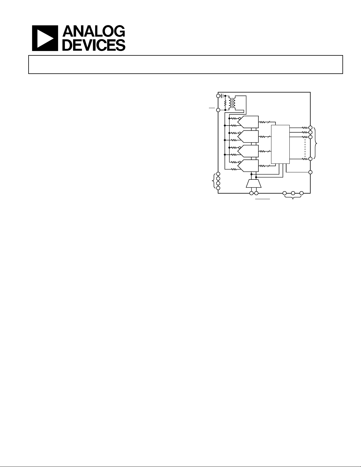
FUNCTIONAL BLOCK DIAGRAM
AIN
AIN
ADC
ADC
ADC
ADC
AGND
NALO
POWER
5VA
3.3VE
AGND
CLOCK DISTRIBUTION
CIRCUIT
Figure 1.
PRODUCT HIGHLIGHTS
1. Guaranteed sample rate of 80 MSPS.
2. Input signal conditioning with optimized noise
performance.
3. Fully tested and guaranteed performance.
AD10678
14
14
DIGITAL
POST-
PROCES-
14
SING
14
DGND DGND
DIGITAL POWERENCODE ENCODE
D
D
3.3V
OUT
OUT
0
15
OUTPUT
DATA
BITS
DRY
03376-A-001
Rev. B
Information furnished by Analog Devices is believed to be accurate and reliable.
However, no responsibility is assumed by Analog Devices for its use, nor for any
infringements of patents or other rights of third parties that may result from its use.
Specifications subject to change without notice. No license is granted by implication
or otherwise under any patent or patent rights of Analog Devices. Trademarks and
registered trademarks are the property of their respective owners.
One Technology Way, P.O. Box 9106, Norwood, MA 02062-9106, U.S.A.
Tel: 781.329.4700
Fax: 781.461.3113 © 2005 Analog Devices, Inc. All rights reserved.
www.analog.com

AD10678
TABLE OF CONTENTS
Specifications..................................................................................... 3
DC Specifications ......................................................................... 3
Digital Specifications ................................................................... 3
AC Specifications.......................................................................... 4
Switching Specifications.............................................................. 5
Absolute Maximum Ratings............................................................ 6
Explanation of Test Levels........................................................... 6
Operating Range........................................................................... 6
ESD Caution.................................................................................. 6
Test Circuits....................................................................................... 7
Pin Configurations and Function Descriptions ........................... 8
Typical Performance Characteristics ...........................................10
REVISION HISTORY
3/05—Rev. A to Rev. B
Changes to Figure 1.......................................................................... 1
Changes to Figure 2 and Figure 3................................................... 7
Added Figure 7 to Figure 9.............................................................. 8
Reformatted Table 7 ......................................................................... 8
Changes to Figure 10........................................................................ 9
Reformatted Theory of Operation Section ................................. 13
Changes to Figure 22...................................................................... 15
Terminology .................................................................................... 12
Theory of Operation ...................................................................... 13
Thermal Considerations............................................................ 13
Input Stage................................................................................... 13
Encoding the AD10678 ............................................................. 13
Output Loading .......................................................................... 13
Analog and Digital Power Supplies.......................................... 13
Analog and Digital Grounding................................................. 14
Other Notes................................................................................. 14
Evaluation Board........................................................................ 14
Outline Dimensions....................................................................... 19
Ordering Guide .......................................................................... 19
12/03—Rev. 0 to Rev. A
Updated format...................................................................Universal
Changes to AC Specifications table footnotes .............................. 4
Changes to Table 1............................................................................ 3
Changes to Table 3............................................................................ 6
Changes to Figure 11...................................................................... 10
Changes to Theory of Operation.................................................. 13
Changes to Ordering Guide.......................................................... 20
2/03—Revision 0: Initial Version
Rev. B | Page 2 of 20

AD10678
SPECIFICATIONS
DC SPECIFICATIONS
AVCC = 5 V, EVCC = 3.3 V, VDD = 3.3 V, TA = 25°C, differential encode = 80 MSPS, C
Table 1.
Parameter Test Level Min Typ Max Unit
RESOLUTION 16 Bits
Offset Error I –0.30 +0.12 +0.30 %FS
Gain Error I –7 +7 %FS
Differential Nonlinearity (DNL) V ±0.7 LSB
Integral Nonlinearity (INL) V ±4 LSB
TEMPERATURE DRIFT
Offset Error V 13 ppm/°C
Gain Error V 200 ppm/°C
POWER SUPPLY REJECTION RATIO (PSRR) V 60 dB
ANALOG INPUTS (AIN, AIN)1
Differential Input Voltage Range V 2.15 V p-p
Differential Input Resistance V 50 Ω
Differential Input Capacitance V 2.5 nF
Input Bandwidth IV 0.40 220 MHz
VSWR2 V 1.04:1 Ratio
POWER SUPPLY3
Supply Current
IAVCC (AVCC = 5.0 V) I 0.95 1.1 A
IEVCC (EVCC = 3.3 V) I 0.15 0.2 A
IVDD (VDD = 3.3 V) I 0.49 0.625 A
Total Power Dissipation4 I 6.86 8.0 W
1
Measurement includes the recommended interface connector.
2
Input VSWR, see . Figure 18
3
Supply voltages should remain stable within ±5% for normal operation.
4
Power dissipation measured with encode at rated speed and –6 dBFS analog input at 10 MHz.
≤ 10 pF, unless otherwise noted.
LOAD
DIGITAL SPECIFICATIONS
AVCC = 5 V, EVCC = 3.3 V, VDD = 3.3 V, TA = 25°C, differential encode = 80 MSPS, C
Table 2.
Parameter Test Level Min Typ Max Unit
ENCODE INPUTS (ENCODE, ENCODE)
Differential Input Voltage Range IV 0.4 V p-p
Differential Input Resistance V 100 Ω
Differential Input Capacitance V 160 pF
LOGIC OUTPUTS (D15 to D0)
Logic Compatibility CMOS
Logic 1 Voltage I
Logic 0 Voltage I
≤100 mA IV 0.9 × VDD V
LOAD
≤100 mA IV 0.4 V
LOAD
Output Coding True binary
Series Output Resistance per Bit 120 Ω
Rev. B | Page 3 of 20
≤ 10 pF, unless otherwise noted.
LOAD

AD10678
AC SPECIFICATIONS
AVCC = 5 V, EVCC = 3.3 V, VDD = 3.3 V, TA = 25°C, differential encode = 80 MSPS, C
Table 3.
Parameter Test Level Min Typ Max Unit
SNR1
Analog Input 2.5 MHz I 77.5 80.5 dBFS
@ −6 dBFS 10 MHz I 77.5 80.5 dBFS
30 MHz I 77 80.2 dBFS
70 MHz I 76 78 dBFS
SINAD2
Analog Input 2.5 MHz I 77.2 80.3 dBFS
@ −6 dBFS 10 MHz I 77.2 80.3 dBFS
30 MHz I 76.6 79.7 dBFS
70 MHz I 74.7 77.4 dBFS
SFDR3
Analog Input 2.5 MHz I 88 97.2 dBFS
@ −6 dBFS 10 MHz I 88 97.2 dBFS
30 MHz I 84 94.2 dBFS
70 MHz I 81 91.7 dBFS
TWO-TONE4
Analog Input
@ −7 dBFS IMD
f1 = 10 MHz, f2 = 12 MHz V 96 dBFS
f1 = 70 MHz, f2 = 72 MHz V 84 dBFS
1
Analog input signal power at −6 dBFS; signal-to-noise (SNR) is the ratio of signal level to total noise (first five harmonics removed). Encode = 80 MSPS. SNR is reported
in dBFS, related back to converter full scale.
2
Analog input signal power at −6 dBFS; signal-to-noise and distortion (SINAD) is the ratio of signal level to total noise + harmonics. Encode = 80 MSPS. SINAD is
reported in dBFS, related back to converter full scale.
3
Analog input signal equals −6 dBFS; SFDR is the ratio of converter full scale to worst spur.
4
Both input tones at −7 dBFS; two-tone intermodulation distortion (IMD) rejection is the ratio of either tone to the worst third-order intermodulation product.
≤ 10 pF, unless otherwise noted.
LOAD
Rev. B | Page 4 of 20

AD10678
SWITCHING SPECIFICATIONS
AVCC = 5 V, EVCC = 3.3 V, VDD = 3.3 V, TA = 25°C, differential encode = 80 MSPS, C
Table 4.
Parameter Test Level Min Typ Max Unit
MAXIMUM CONVERSION RATE I 80 MSPS
MINIMUM CONVERSION RATE IV 30 MSPS
DUTY CYCLE IV 40 60 %
ENCODE INPUTS PARAMETERS
Encode Period @ 80 MSPS, t
Encode Pulse Width High @ 80 MSPS, t
Encode Pulse Width Low @ 80 MSPS, t
V 12.5 ns
ENC
V 6.25 ns
ENCH
V 6.25 ns
ENCL
ENCODE/DATA (D15:D0)
Propagation Delay, t
Valid Time, t
7.3 ns
PDL
6.7 ns
PDH
ENCODE/DATA READY1
Encode Rising to Data Ready Falling, t
Encode Rising to Data Ready Rising, t
12.6 ns
DR_F
6.4 ns
DR_R
DATA READY/DATA1
Data Ready to Data (Hold Time) t
Data Ready to Data (Setup Time) t
10 ns
H_DR
1 ns
S_DR
APERTURE DELAY, tA V 480 ps
APERTURE UNCERTAINTY (JITTER), tJ V 500 fs rms
PIPELINE DELAYS V 10 Cycles
1
Duty cycle = 50%.
≤ 10 pF, unless otherwise noted.
LOAD
Rev. B | Page 5 of 20

AD10678
ABSOLUTE MAXIMUM RATINGS
Table 5.
Parameter Rating
AVCC to AGND 0 V to 7 V
EVCC to AGND 0 V to 6 V
V
to DGND –0.5 V to +3.8 V
DD
Analog Input Voltage 0 V to AVCC
Analog Input Current 25 mA
Encode Input Voltage 0 V to 5 V
Digital Output Voltage –0.5 V to VDD
Maximum Junction Temperature 150°C
Storage Temperature Range Ambient –65°C to +150°C
Maximum Operating Temperature Ambient 92°C
Table 6. Output Coding (True Binary)
Code AIN (V) Digital Output
65535 +1.1 1111 1111 1111 1111
. . .
. . .
. . .
32768 0 1000 0000 0000 0000
32767 –0.000034 0111 1111 1111 1111
. . .
. . .
. . .
0 –1.1 0000 0000 0000 0000
Stresses above those listed under Absolute Maximum Ratings
may cause permanent damage to the device. This is a stress
rating only; functional operation of the device at these or any
other conditions above those indicated in the operational
section of this specification is not implied. Exposure to absolute
maximum rating conditions for extended periods may affect
device reliability.
EXPLANATION OF TEST LEVELS
I. 100% production tested.
II. 100% production tested at 25°C and sample tested at
specified temperatures.
III. Sample tested only.
IV. Parameter is guaranteed by design and characterization
testing.
V. Parameter is a typical value only.
100% production tested at 25°C; guaranteed by design and
characterization testing for industrial temperature range; 100%
production tested at temperature extremes for military devices.
OPERATING RANGE
Operating ambient temperature range: 0°C to 70°C. See the
Thermal Considerations section.
ESD CAUTION
ESD (electrostatic discharge) sensitive device. Electrostatic charges as high as 4000 V readily accumulate on the
human body and test equipment and can discharge without detection. Although this product features
proprietary ESD protection circuitry, permanent damage may occur on devices subjected to high energy
electrostatic discharges. Therefore, proper ESD precautions are recommended to avoid performance
degradation or loss of functionality.
Rev. B | Page 6 of 20
 Loading...