ANALOG DEVICES AD10465 Service Manual
Dual Channel, 14-Bit, 65 MSPS A/D Converter
A
A
A3A
A
FEATURES
Dual, 65 MSPS minimum sample rate
Channel-to-channel matching, ±0.5% gain error
Channel-to-channel isolation, >90 dB
DC-coupled signal conditioning included
Selectable bipolar input voltage range
(±0.5 V, ±1.0 V, ±2.0 V)
Gain flatness up to 25 MHz: <0.2 dB
80 dB spurious-free dynamic range
Twos complement output format
3.3 V or 5 V CMOS-compatible output levels
1.75 W per channel
Industrial and military grade
APPLICATIONS
Phased array receivers
Communications receivers
FLIR processing
Secure communications
GPS antijamming receivers
Multichannel, multimode receivers
GENERAL DESCRIPTION
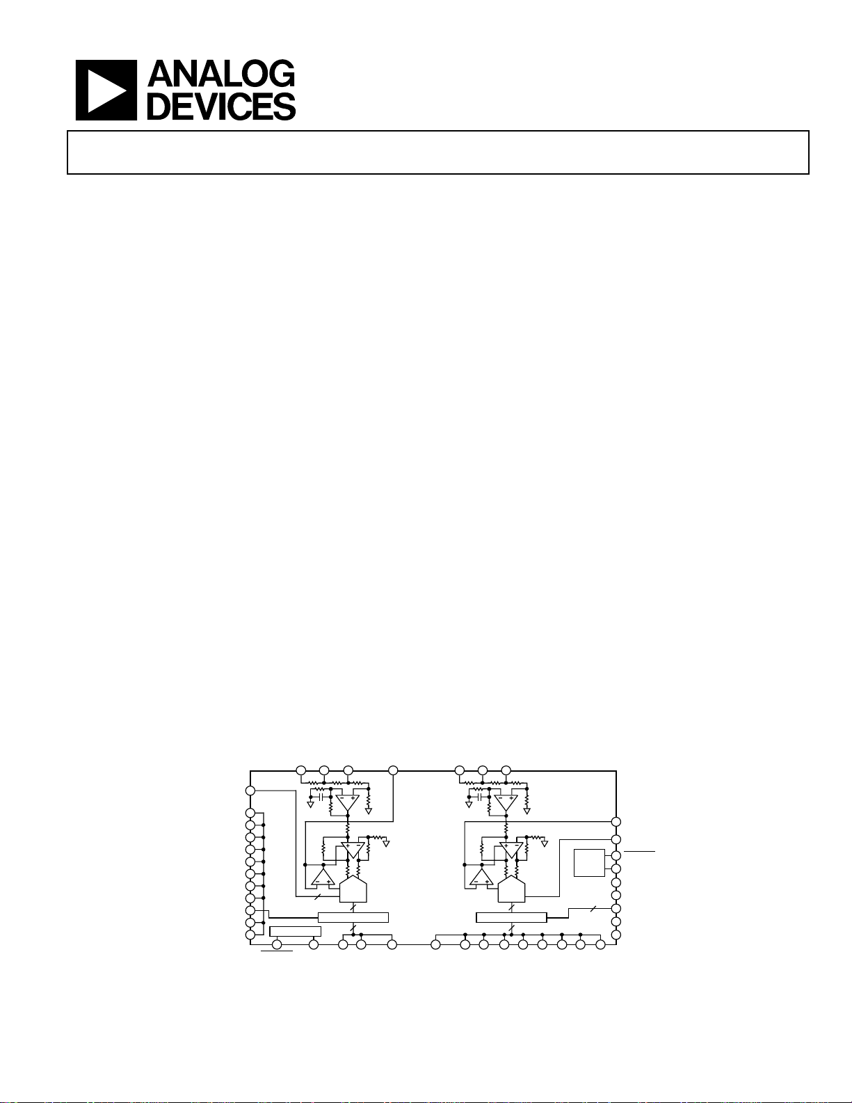
The AD10465 is a full channel ADC solution with on-module
signal conditioning for improved dynamic performance and
fully matched channel-to-channel performance. The module
includes two wide dynamic range AD6644 ADCs. Each
AD6644 has a dc-coupled amplifier front end including an
AD8037 low distortion, high bandwidth amplifier that provides
high input impedance and gain and drives the AD8138 singleto-differential amplifier. The AD6644s have on-chip track-andhold circuitry and utilize an innovative multipass architecture
to achieve 14-bit, 65 MSPS performance.
FUNCTIONAL BLOCK DIAGRAM
DRAOUT
D0A (LSB)
D1A
D2A
D3A
D4A
D5A
D6A
D7A
D8A
D9A
D10A
12
15
16
17
18
19
20
21
22
23
24
25
28
ENCODEA
AINA38AINA27A
TIMING
29 31 32 33 34 35 36 37 38 39 40 41 42
ENCODEA
1
REF_
IN
6
VREF
DROUT
11
14
OUTPUT BUFFERING
3
D11 D12A D13A (MS BA) D0B (LSBB) D 1B D2B D3B D4B D5B D6B D7B D8B
with Analog Input Signal Conditioning
AD10465
The AD10465 uses innovative high density circuit design and laser
trimmed, thin film resistor networks to achieve exceptional
matching and performance, while still maintaining excellent
isolation and providing for significant board area savings.
The AD10465 operates with ±5.0 V supplies for the analog
signal conditioning with a separate 5.0 V supply for the analogto-digital conversion and 3.3 V digital supply for the output
stage. Each channel is completely independent, allowing
operation with independent encode and analog inputs. The
AD10465 also offers the user a choice of analog input signal
ranges to further minimize additional external signal
conditioning, while remaining general-purpose.
The AD10465 is packaged in a 68-lead ceramic leaded chip
carrier package, footprint-compatible with the earlier
generation AD10242 (12-bit, 40 MSPS) and AD10265 (12-bit,
65 MSPS). Manufacturing is done on the Analog Devices Mil38534 Qualified Manufacturers Line (QML) and components
are available up to Class-H (−40°C to +85°C). The AD6644
internal components are manufactured on Analog Devices’ high
speed complementary bipolar process (XFCB).
PRODUCT HIGHLIGHTS
1. Guaranteed sample rate of 65 MSPS.
2. Input amplitude options, user configurable.
3. Input signal conditioning included; both channels matched
for gain.
4. Fully tested/characterized performance.
5. Footprint-compatible family; 68-lead CLCC package.
B3
B2
B1
IN
IN
63
62
VREF
DROUT
14
OUTPUT BUFFERING
9
TIMING
5
56
REF_B
DRBOUT
55
52
ENCODEB
51
ENCODEB
D13B (MSBB)
49
48
D12B
47
D11B
46
D10B
45
D9B
02356-001
AD10465
Figure 1.
IN
64
Rev. A
Information furnished by Analog Devices is believed to be accurate and reliable. However, no
responsibility is assumed by Anal og Devices for its use, nor for any infringements of patents or ot her
rights of third parties that may result from its use. Specifications subject to change without notice. No
license is granted by implication or otherwise under any patent or patent rights of Analog Devices.
Trademarks and registered trademarks are the property of their respective owners.
One Technology Way, P.O. Box 9106, Norwood, MA 02062-9106, U.S.A.
Tel: 781.329.4700 www.analog.com
Fax: 781.461.3113 ©2006 Analog Devices, Inc. All rights reserved.

AD10465
TABLE OF CONTENTS
Features.............................................................................................. 1
Theory of Operation ...................................................................... 12
Applications....................................................................................... 1
General Description ......................................................................... 1
Product Highlights....................................................................... 1
Functional Block Diagram .............................................................. 1
Revision History ............................................................................... 2
Specifications..................................................................................... 3
Test Circuits....................................................................................... 6
Absolute Maximum Ratings............................................................ 7
ESD Caution.................................................................................. 7
Pin Configuration and Pin Function Descriptions...................... 8
Typical Performance Characteristics ............................................. 9
Terminology .................................................................................... 11
REVISION HISTORY
Using the Flexible Input ............................................................ 12
Applying the AD10465.................................................................. 13
Encoding the AD10465 ............................................................. 13
Jitter Considerations .................................................................. 13
Power Supplies............................................................................ 14
Output Loading .......................................................................... 14
Layout Information.................................................................... 14
Evaluation Board............................................................................ 15
Bill Of Materials List for AD10465 Evaluation Board........... 19
Silkscreens ................................................................................... 20
Outline Dimensions....................................................................... 24
Ordering Guide .......................................................................... 24
3/06—Rev. 0 to Rev. A
Remove AZ Grade..............................................................Universal
Changes to General Description Section ...................................... 1
Changes to Table 1............................................................................ 3
Inserted Test Circuits Section ......................................................... 6
Updates to Ordering Guide........................................................... 24
2001—Revision 0: Initial Version
Rev. A | Page 2 of 24

AD10465
SPECIFICATIONS
AVCC = +5 V; AVEE = –5 V; DVCC = 3.3 V applies to each ADC, unless otherwise noted. All specifications guaranteed within 100 ms of
initial power-up, regardless of sequencing.
Table 1.
Test1 Mil AD10465BZ/QML-H
Parameter Temp Level Subgroup Min Typ Max Unit
RESOLUTION 14 Bits
DC ACCURACY
No Missing Codes Full VI 1, 2, 3 Guaranteed
Offset Error 25°C I 1 −2.2 ±0.02 +2.2 % FS
Full VI 2, 3 −2.2 ±1.0 +2.2 % FS
Offset Error Channel Match Full V −1 ±1.0 +1 %
Gain Error2 25°C I 1 −3 −1.0 +1 % FS
Full VI 2, 3 −5 ±2.0 +5 % FS
Gain Error Channel Match 25°C I 1 −1.5 ±0.5 +1.5 %
Max I 2 −3 ±1.0 +3 %
Min I 3 −5 +5 %
ANALOG INPUT (AIN)
Input Voltage Range
AIN1 Full V ±0.5 V
AIN2 Full V ±1.0 V
AIN3 Full V ±2 V
Input Resistance
AIN1 Full IV 12 99 100 101 Ω
AIN2 Full IV 12 198 200 202 Ω
AIN3 Full IV 12 396 400 404 Ω
Input Capacitance3 25°C IV 12 0 4.0 7.0 pF
Analog Input Bandwidth4 Full V 100 MHz
ENCODE INPUT (ENC, ENC)5
Differential Input Voltage Full IV 0.4 V p-p
Differential Input Resistance 25°C V 10 kΩ
Differential Input Capacitance 25°C V 2.5 pF
SWITCHING PERFORMANCE
Maximum Conversion Rate6 Full VI 4, 5, 6 65 MSPS
Minimum Conversion Rate6 Full V 12 20 MSPS
Aperture Delay (tA) 25°C V 1.5 ns
Aperture Delay Matching 25°C IV 12 250 500 ps
Aperture Uncertainty (Jitter) 25°C V 0.3 ps rms
ENCODE Pulse Width High 25°C IV 12 6.2 7.7 9.2 ns
ENCODE Pulse Width Low 25°C IV 12 6.2 7.7 9.2 ns
Output Delay (tOD) Full V 6.8 ns
ENCODE, Rising to Data Ready, Rising Delay (T
SNR7
Analog Input @ 4.98 MHz 25°C V 70 dBFS
Analog Input @ 9.9 MHz 25°C I 4 69 70 dBFS
Full II 5, 6 68 70 dBFS
Analog Input @ 19.5 MHz 25°C I 4 68 70 dBFS
Full II 5, 6 67 70 dBFS
Analog Input @ 32.1 MHz 25°C I 4 67 69 dBFS
Full II 5, 6 67 69 dBFS
E_DR
) Full 11.5 ns
Rev. A | Page 3 of 24

AD10465
Test1 Mil AD10465BZ/QML-H
Parameter Temp Level Subgroup Min Typ Max Unit
SINAD8
Analog Input @ 4.98 MHz 25°C V 70 dB
Analog Input @ 9.9 MHz 25°C I 4 67.5 69 dB
Full II 5, 6 67.5 69 dB
Analog Input @ 19.5 MHz 25°C I 4 65 68 dB
Full II 5, 6 65 68 dB
Analog Input @ 32.1 MHz 25°C I 4 60 63 dB
Full II 5, 6 58 61 dB
SPURIOUS-FREE DYNAMIC RANGE9
Analog Input @ 4.98 MHz 25°C V 85 dBFS
Analog Input @ 9.9 MHz 25°C I 4 73 82 dBFS
Full II 5, 6 70 82 dBFS
Analog Input @ 19.5 MHz 25°C I 4 72 78 dBFS
Full II 5, 6 70 78 dBFS
Analog Input @ 32.1 MHz 25°C I 4 62 68 dBFS
Full II 5, 6 60 66 dBFS
TWO-TONE IMD REJECTION10
fIN = 10 MHz and 11 MHz 25°C I 4 78 87 dBFS
f1 and f2 are −7 dB II 5, 6 78 dBFS
fIN = 31 MHz and 32 MHz 25°C I 4 68 70 dBFS
f1 and f2 Are −7 dB Full II 5, 6 60 dBFS
CHANNEL-TO-CHANNEL ISOLATION11 25°C IV 12 90 dB
TRANSIENT RESPONSE 25°C V 15.3 ns
OVERVOLTAGE RECOVERY TIME
VIN = 2.0 × fS Full IV 12 40 100 ns
VIN = 4.0 × fS Full IV 12 150 200 ns
DIGITAL OUTPUTS12
Logic Compatibility CMOS
DVCC = 3.3 V
Logic 1 Voltage Full I 1, 2, 3 2.5 DVCC − 0.2 V
Logic 0 Voltage Full I 1, 2, 3 0.2 0.5 V
DVCC = 5 V
Logic 1 Voltage Full V DVCC − 0.3 V
Logic 0 Voltage Full V 0.35 V
Output Coding Twos complement
POWER SUPPLY
AVCC Supply Voltage13 Full VI 4.85 5.0 5.25 V
I (AVCC) Current Full I 270 308 mA
AVEE Supply Voltage13 Full VI −5.25 −5.0 −4.75 V
I (AVEE) Current Full V 38 49 mA
DVCC Supply Voltage13 Full VI 3.135 3.3 3.465 V
I (DVCC) Current Full V 30 46 mA
ICC (Total) Supply Current per Channel Full I 1, 2, 3 338 403 mA
Power Dissipation (Total) Full I 1, 2, 3 3.5 3.9 W
Power Supply Rejection Ratio (PSRR) Full V 0.02 % FSR/% VS
Passband Ripple to 10 MHz V 0.1 dB
Passband Ripple to 25 MHz V 0.2 dB
Rev. A | Page 4 of 24

AD10465
1
See Table 3.
2
Gain tests are performed on AIN1 input voltage range.
3
Input capacitance specification combines AD8037 die capacitance and ceramic package capacitance.
4
Full power bandwidth is the frequency at which the spectral power of the fundamental frequency (as determined by FFT analysis) is reduced by 3 dB.
5
All ac specifications tested by driving
6
Minimum and maximum conversion rates allow for variation in encode duty cycle of 50% ± 5%.
7
Analog input signal power at –1 dBFS; signal-to-noise ratio (SNR) is the ratio of signal level to total noise (first five harmonics removed). ENCODE = 65 MSPS. SNR is
reported in dBFS, related back to converter full power.
8
Analog input signal power at –1 dBFS. Signal-to-noise and distortion (SINAD) is the ratio of signal level to total noise + harmonics. ENCODE = 65 MSPS.
9
Analog input signal power swept from −1 dBFS to −60 dBFS; SFDR is the ratio of converter full scale to worst spur.
10
Both input tones at −7 dBFS; two-tone intermodulation distortion (IMD) rejection is the ratio of either tone to the worst third order intermodulation product.
11
Channel-to-channel isolation tested with A channel grounded and a full-scale signal applied to B channel.
12
Digital output logic levels: DVCC = 3.3 V, C
13
Supply voltage recommended operating range. AVCC can be varied from 4.85 V to 5.25 V. However, rated ac (harmonics) performance is valid only over the range
AV
= 5.0 V to 5.25 V.
CC
ENCODE
and ENCODE differentially.
= 10 pF. Capacitive loads > 10 pF degrade performance.
LOAD
Rev. A | Page 5 of 24
AD10465
A
V
A
A
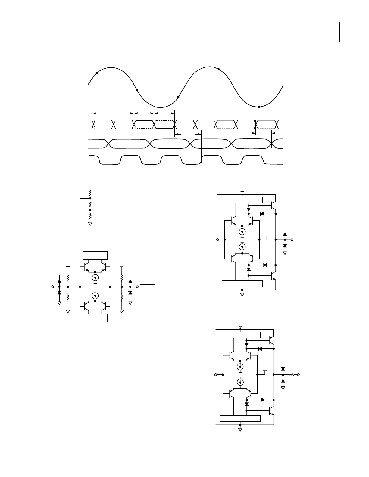
TEST CIRCUITS
t
A
N
A
IN
N+1
N+2
N+3
t
ENC
ENC, ENC
D[13:0]
DRY
N
3
IN
VIN2
VIN1
200Ω
100Ω
100Ω
TO AD8037
02356-016
Figure 3. Analog Input Stage
LOADS
10kΩ
10kΩ
AV
CC
AV
CC
AV
CC
10kΩ
ENCODE ENCO DE
10kΩ
t
ENCH
N+1 N+2 N+3 N+4
N–3 N–2 N–1 N
t
ENCL
t
E, DR
Figure 2. Timing Diagram
DV
CC
CURRENT MIRROR
AV
CC
CURRENT MIRROR
Figure 5. Digital Output Stage
N+4
t
OD
02356-015
DV
CC
V
REF
DR_OUT
02356-018
LOADS
02356-017
Figure 4. ENCODE Inputs
DV
CC
CURRENT MIRROR
DV
CC
V
REF
CURRENT MIRROR
100Ω
D0 TO
D13
02356-019
Figure 6. Digital Output Stage
Rev. A | Page 6 of 24
AD10465
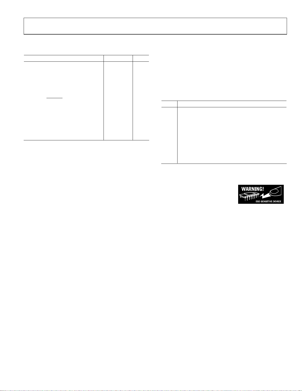
ABSOLUTE MAXIMUM RATINGS
Table 2.
Parameter Min Max Units
ELECTRICAL
VCC Voltage 0 +7 V
V
Voltage –7 0 V
EE
Analog Input Voltage VEE VCC V
Analog Input Current −10 +10 mA
Digital Input Voltage (ENCODE) 0 VCC V
ENCODE, ENCODE
Digital Output Current −10 +10 mA
ENVIRONMENTAL1
Operating Temperature Range (Case) −40 +85 °C
Maximum Junction Temperature 174 °C
Lead Temperature (Soldering, 10 sec) 300 °C
Storage Temperature Range (Ambient) −65 +150 °C
1
Typical thermal impedance for 68-lead CLCC package: θJC = 2.2°C/W; θJA =
24.3°C/W.
Differential Voltage
4 V
Stresses above those listed under Absolute Maximum Ratings
may cause permanent damage to the device. This is a stress
rating only; functional operation of the device at these or any
other conditions above those indicated in the operational
section of this specification is not implied. Exposure to absolute
maximum rating conditions for extended periods may affect
device reliability.
Table 3. Test Levels
Level Description
I 100% production tested.
II
III Sample tested only.
IV
V Parameter is a typical value only.
VI
100% production tested at 25°C, and sample tested at
specified temperatures. AC testing done on sample
basis.
Parameter is guaranteed by design and characterization
testing.
100% production tested at 25°C, sample tested at
temperature extremes.
ESD CAUTION
ESD (electrostatic discharge) sensitive device. Electrostatic charges as high as 4000 V readily accumulate on
the human body and test equipment and can discharge without detection. Although this product features
proprietary ESD protection circuitry, permanent damage may occur on devices subjected to high energy
electrostatic discharges. Therefore, proper ESD precautions are recommended to avoid performance
degradation or loss of functionality.
Rev. A | Page 7 of 24
AD10465
A
A
D
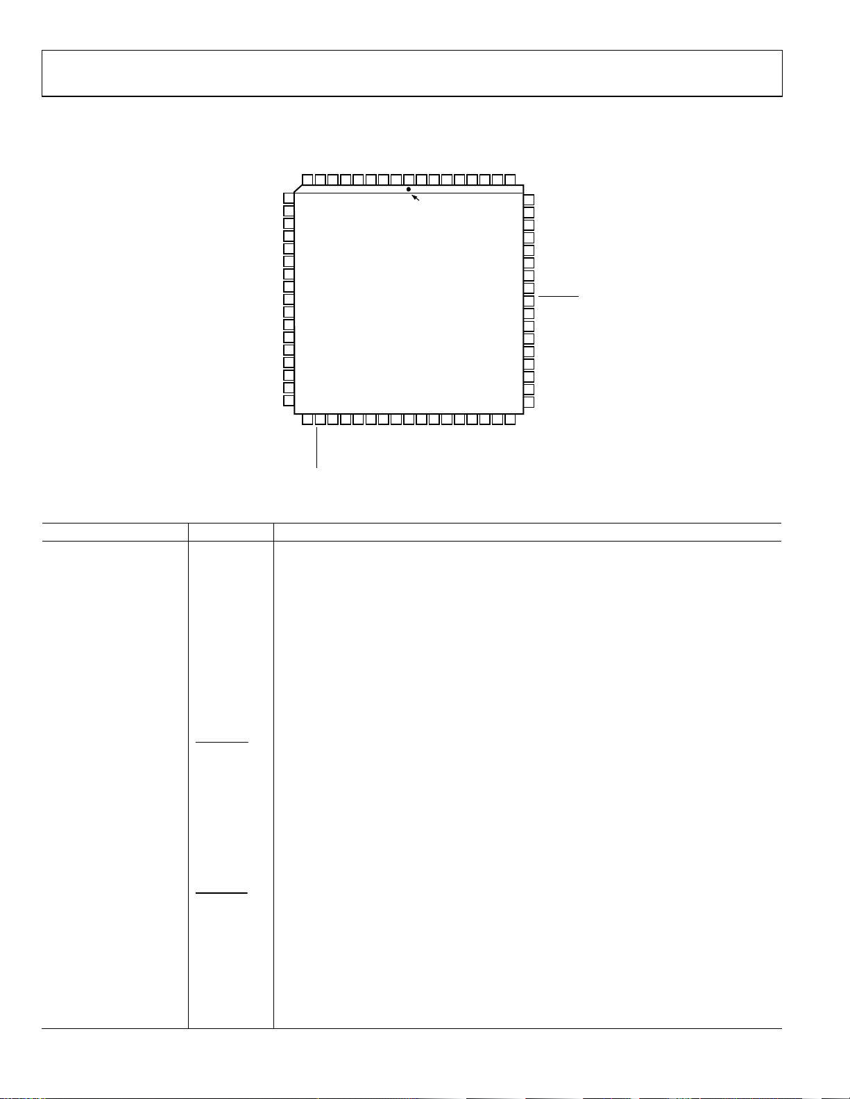
PIN CONFIGURATION AND PIN FUNCTION DESCRIPTIONS
B1
B2
A1
A2
A3
IN
IN
AGNDA
AGNDA
DRAOUT
AV
AV
D0A (LSBA)
D1A
D2A
D3A
D4A
D5A
D6A
D7A
D8A
D9A
D10A
DGNDA
IN
A
A
A
AGND
10
11
12
13
EE
14
CC
15
16
17
18
19
20
21
22
23
24
25
26
27 28 29 30 31 32 33 34 35 36 37 38 39 40 41 42 43
CC
DV
DGNDA
ENCODEA
ENCODEA
AGNDAAGNDAREF_A
D12A
D11A
AGND
AGNDB
SHIEL
123456789 6867666564636261
PIN 1
IDENTIFIER
AD10465
TOP VIEW
(Not to Scale)
D1B
D2B
D0B (LSBB)
D13A (MSBA)
Figure 7. Pin Configuration
Table 4. Pin Function Descriptions
Pin No. Mnemonic Description
1 SHIELD Internal Ground Shield Between Channels.
2, 4, 5, 9 to11 AGNDA
A Channel Analog Ground. A ground and B ground should be connected as close to the device
as possible.
3 REF_A A Channel Internal Voltage Reference.
6 AINA1 Analog Input for A Side ADC (Nominally ±0.5 V).
7 AINA2 Analog Input for A Side ADC (Nominally ±1.0 V).
8 AINA3 Analog Input for A Side ADC (Nominally ±2.0 V).
12 DRAOUT Data Ready A Output.
13 AVEE Analog Negative Supply Voltage (Nominally −5.0 V or −5.2 V).
14 AVCC Analog Positive Supply Voltage (Nominally 5.0 V).
26, 27 DGNDA A Channel Digital Ground.
15 to 25, 31 to 33 D0A to D13A Digital Outputs for ADC A. D0A (LSBA).
28
ENCODEA
Complement of ENCODE.
29 ENCODEA Data Conversion Initiated on Rising Edge of ENCODE Input.
30 DVCC Digital Positive Supply Voltage (Nominally 5.0 V or 3.3 V).
43, 44 DGNDB B Channel Digital Ground.
34 to 42, 45 to 49 D0B to D13B Digital Outputs for ADC B. D0B (LSBB).
53, 54, 57 to 61, 65, 68 AGNDB
B Channel Analog Ground. A ground and B ground should be connected as close to the device
as possible.
50 DVCC Digital Positive Supply Voltage (Nominally 5.0 V or 3.3 V).
51 ENCODEB Data conversion initiated on rising edge of ENCODE input.
52
ENCODEB
Complement of ENCODEB.
55 DRBOUT Data Ready B Output.
56 REF_B B Channel Internal Voltage Reference.
62 AINB1 Analog Input for B Side ADC (Nominally ±0.5 V).
63 AINB2 Analog Input for B Side ADC (Nominally ±1.0 V).
64 AINB3 Analog Input for B Side ADC (Nominally ±2.0 V).
66 AVCC Analog Positive Supply Voltage (Nominally 5.0 V).
67 AVEE Analog Negative Supply Voltage (Nominally −5.0 V or −5.2 V).
Rev. A | Page 8 of 24
AVEEAVCCAGNDB
D3B
D4B
D5B
B3
IN
A
D6B
IN
A
D7B
IN
A
D8B
AGNDB
60
59
58
57
56
55
54
53
52
51
50
49
48
47
46
45
44
DGNDB
AGNDB
AGNDB
AGNDB
AGNDB
REF_B
DRBOUT
AGNDB
AGNDB
ENCODEB
ENCODEB
DV
CC
D13B (MSBB)
D12B
D11B
D10B
D9B
DGNDB
02356-002
 Loading...