Dual, 12-Bit, 40 MSPS MCM A/D Converter
a
with Analog Input Signal Conditioning
FEATURES
Two Matched ADCs with Input Signal Conditioning
Selectable Bipolar Input Voltage Range
(ⴞ0.5 V, ⴞ1.0 V, ⴞ2.0 V)
Full MIL-STD-883B Compliant
80 dB Spurious-Free Dynamic Range
Trimmed Channel-Channel Matching
APPLICATIONS
Radar Processing
Communications Receivers
FLIR Processing
Secure Communications
Any I/Q Signal Processing Application
PRODUCT DESCRIPTION
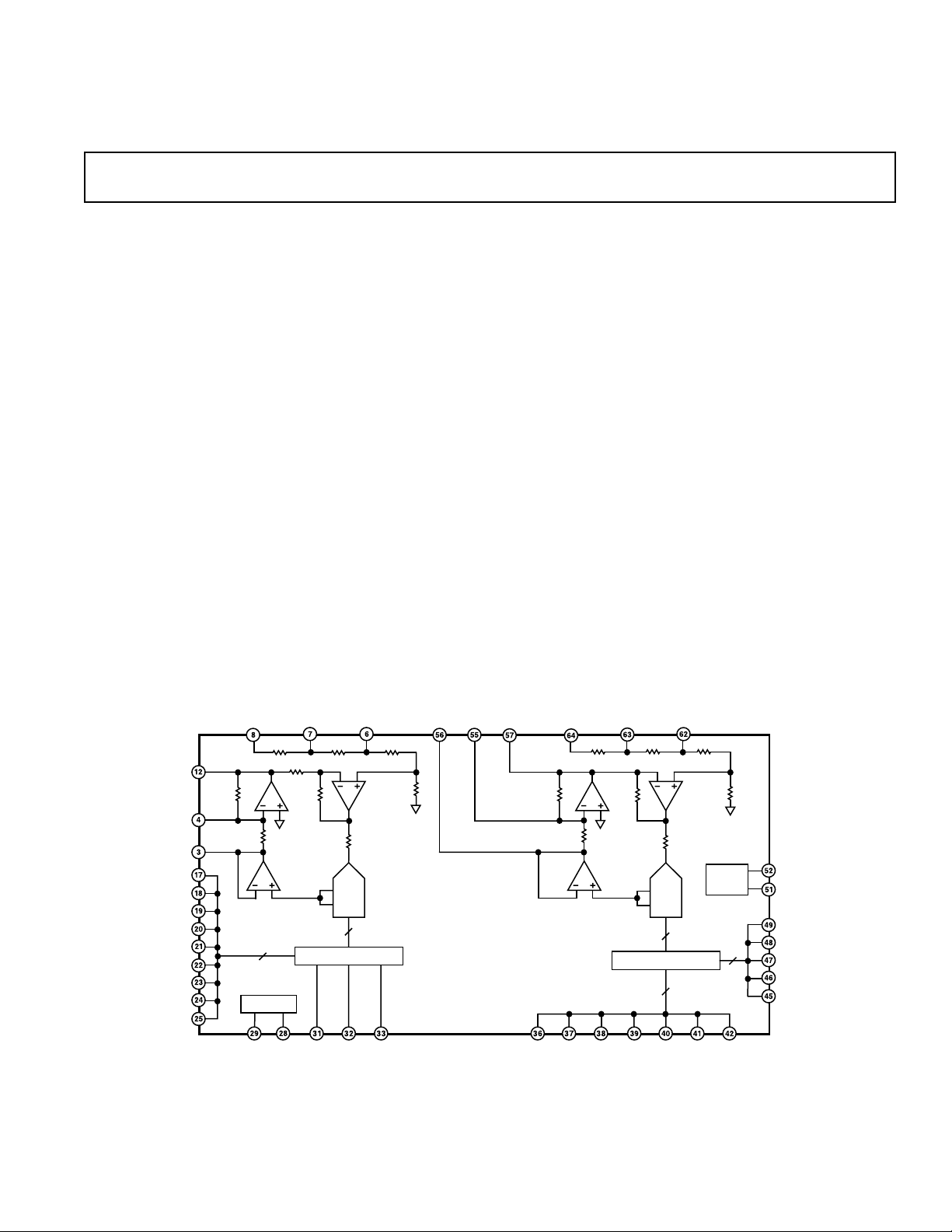
The AD10242 is a complete dual signal chain solution including
onboard amplifiers, references, ADCs, and output buffering providing unsurpassed total system performance. Each channel is
laser trimmed for gain and offset matching and provides channelto-channel crosstalk performance better than 80 dB. The AD10242
utilizes two each of the AD9632, OP279, and AD9042 in a custom MCM to gain space, performance, and cost advantages over
solutions previously available.
AD10242
The AD10242 operates with ±5.0 V for the analog signal conditioning with a separate 5.0 V supply for the analog-to-digital
conversion. Each channel is completely independent, allowing
operation with independent encode or analog inputs. The AD10242
also offers the user a choice of analog input signal ranges to minimize additional signal conditioning required for multiple functions
within a single system. The heart of the AD10242 is the AD9042,
which is designed specifically for applications requiring wide
dynamic range.
The AD10242 is manufactured by Analog Devices on our
MIL-PRF-38534 MCM line and is completely qualified. Units
are packaged in a custom cofired ceramic 68-lead gull wing
package and specified for operation from –55°C to +125°C.
Contact the factory for additional custom options including those
which allow the user to ac couple the ADC directly, bypassing
the front end amplifier section. Also see the AD9042 data sheet
for additional details on ADC performance.
PRODUCT HIGHLIGHTS
1. Guaranteed sample rate of 40 MSPS.
2. Dynamic performance specified over entire Nyquist band;
spurious signals @ 80 dBc for –1 dBFS input signals.
3. Low power dissipation: <2 W off ±5.0 V supplies.
4. User defined input amplitude.
5. Packaged in 68-lead ceramic leaded chip carrier.
FUNCTIONAL BLOCK DIAGRAM
2AIN1
A
3
UPOS
UCOM
UNEG
(LSB) D0A
D1A
D2A
D3A
D4A
D5A
D6A
D7A
D8A
A
IN
TIMING
ENC
OP279
OP279
9
OUTPUT BUFFERING
ENC
IN
AD9632
AD9042
V
REF
12
D9A D10A D11A
(MSB)
AD10242
REV. B
Information furnished by Analog Devices is believed to be accurate and
reliable. However, no responsibility is assumed by Analog Devices for its
use, nor for any infringements of patents or other rights of third parties that
may result from its use. No license is granted by implication or otherwise
under any patent or patent rights of Analog Devices.
A
A
UPOSUNEG UCOM
One Technology Way, P.O. Box 9106, Norwood, MA 02062-9106, U.S.A.
Tel: 781/329-4700 www.analog.com
Fax: 781/326-8703 © Analog Devices, Inc., 2001
AIN3
OP279
D0B
D1B D2B D3B D4B D5B D6B
(LSB)
2
IN
OP279
AD9042
OUTPUT BUFFERING
1
IN
AD9632
TIMING
V
REF
12
5
7
ENC
ENC
D11B (MSB)
D10B
D9B
D8B
D7B

AD10242–SPECIFICATIONS
Electrical Characteristics
(AVCC = 5 V; AVEE = –5.0 V; DVCC = 5 V; applies to each ADC unless otherwise noted.)
Test Mil AD10242BZ/TZ
Parameter Temp Level Subgroup Min Typ Max Unit
RESOLUTION 12 Bits
DC ACCURACY
No Missing Codes Full VI 1, 2, 3 Guaranteed
Offset Error 25°C I 1 –0.5 ± 0.05 +0.5 % FS
Full VI 2, 3 –2.0 ± 1.0 +2.0 % FS
Offset Error Channel Match Full V ± 0.1 %
Gain Error
1
25°C I 1 –1.0 ± 0.5 +1.0 % FS
Full VI 2, 3 –1.5 ± 0.8 +1.5 % FS
Gain Error Channel Match Full V ± 0.1 %
ANALOG INPUT (A
)
IN
Input Voltage Range
1 Full I ± 0.5 V
A
IN
A
2 Full I ± 1.0 V
IN
3 Full I ± 2V
A
IN
Input Resistance
AIN1 Full IV 12 99 100 101 Ω
2 Full IV 12 198 200 202 Ω
A
IN
3 Full IV 12 396 400 404 Ω
A
IN
Input Capacitance
Analog Input Bandwidth
ENCODE INPUT
4, 5
2
3
25°C IV 12 0 4.0 7.0 pF
Full V 60 MHz
Logic Compatibility TTL/CMOS
Logic “1” Voltage Full I 1, 2, 3 2.0 5.0 V
Logic “0” Voltage Full I 1, 2, 3 0 0.8 V
Logic “1” Current (V
Logic “0” Current (V
= 5 V) Full I 1, 2, 3 625 800 µA
INH
= 0 V) Full I 1, 2, 3 –400 –300 µA
INL
Input Capacitance 25° C V 12 7.0 pF
SWITCHING PERFORMANCE
Maximum Conversion Rate
Minimum Conversion Rate
Aperture Delay (t
)25°C V 1.0 ns
A
6
6
Full VI 4, 5, 6 40 50 MSPS
Full V 12 5 MSPS
Aperture Delay Matching 25°CV ± 2.0 ns
Aperture Uncertainty (Jitter) 25°C V 1 ps rms
ENCODE Pulsewidth High 25°CIV 12 12 10 ns
ENCODE Pulsewidth Low 25°CIV 12 10 41ns
Output Delay (tOD) Full IV 12 10 12 14 ns
7
SNR
Analog Input @ 1.2 MHz 25°CV 68 dB
@ 4.85 MHz 25°CI 4 63 66 dB
Full II 5, 6 62 66 dB
@ 9.9 MHz 25°CI 4 63 65 dB
Full II 5, 6 62 65 dB
@ 19.5 MHz 25°CI 4 60 63 dB
Full II 5, 6 59 62 dB
8
SINAD
Analog Input @ 1.2 MHz 25°CV 67 dB
@ 4.85 MHz 25°CI 4 62 65 dB
Full II 5, 6 61 64 dB
@ 9.9 MHz 25°CI 4 60 64 dB
Full II 5, 6 60 63 dB
@ 19.5 MHz 25°CI 4 58 61 dB
Full II 5, 6 58 60 dB
–2–
REV. B

AD10242
Test Mil AD10242BZ/TZ
Parameter Temp Level Subgroup Min Typ Max Unit
SPURIOUS-FREE DYNAMIC RANGE
Analog Input @ 1.2 MHz 25°C I 81 dBFS
@ 4.85 MHz 25°C I 4 70 80 dBFS
@ 9.9 MHz 25°C I 4 63 70 dBFS
@ 19.5 MHz 25°C I 4 60 67 dBFS
TWO-TONE IMD REJECTION
F1, F2 @ –7 dBFS Full II 4, 5, 6 70 76 dBc
CHANNEL-TO-CHANNEL ISOLATION
TRANSIENT RESPONSE 25°CV 10 ns
LINEARITY
Differential Nonlinearity 25°C IV 12 0.3 1.0 LSB
(Encode = 20 MHz) Full IV 12 0.5 1.25 LSB
Integral Nonlinearity 25°C V 0.3
(
Encode
= 20 MHz) Full V 0.5 LSB
OVERVOLTAGE RECOVERY TIME
V
= 2.0 × FS Full IV 12 50 100 ns
IN
VIN = 4.0 × FS
DIGITAL OUTPUTS
Logic Compatibility CMOS
Logic “1” Voltage
Logic “0” Voltage
13
14
Output Coding Two’s Complement
POWER SUPPLY
Supply Voltage Full VI 5.0 V
AV
CC
) Current Full V 260 mA
I (AV
CC
AV
Supply Voltage Full VI –5.0 V
EE
) Current Full V 55 mA
I (AV
EE
Supply Voltage Full VI 5.0 V
DV
CC
I (DV
I
) Current Full V 25 mA
CC
(Total) Supply Current Full I 1, 2, 3 350 400 mA
CC
Power Dissipation (Total) Full I 1, 2, 3 1.75 2.0 W
Power Supply Rejection Ratio (PSRR) Full I 7, 8 0.01 0.02 % FSR/% V
Pass Band Ripple to 10 MHz Full IV 12 0.2 dB
NOTES
1
Gain tests are performed on AIN3 over specified input voltage range.
2
Input capacitance specifications combine AD9632 die capacitance and ceramic package capacitance.
3
Full power bandwidth is the frequency at which the spectral power of the fundamental frequency (as determined by FFT analysis) is reduced by 3 dB.
4
ENCODE driven by single-ended source; ENCODE bypassed to ground through 0.01 µF capacitor.
5
ENCODE may also be driven differentially in conjunction with ENCODE; see Encoding the AD10242 section for details.
6
Minimum and maximum conversion rates allow for variation in Encode Duty Cycle of 50% ± 5%.
7
Analog Input signal power at –1 dBFS; signal-to-noise ratio (SNR) is the ratio of signal level to total noise (first 5 harmonics removed). Encode = 40.0 MSPS.
8
Analog Input signal power at –1 dBFS; signal-to-noise and distortion (SINAD) is the ratio of signal level to total noise + harmonics. Encode = 40.0 MSPS.
9
Analog Input signal equal –1 dBFS; SFDR is ratio of converter full scale to worst spur.
10
Both input tones at –7 dBFS; two-tone intermodulation distortion (IMD) rejection is the ratio of either tone to the worst third order intermod product. f1 = 10.0 MHz
± 100 kHz, 50 kHz ≤ f1 – f2 ≤ 300 kHz.
11
Channel-to-channel isolation tested with A channel grounded and a full-scale signal applied to B channel (AIN1).
12
Input driven to 2× and 4× AIN1 range for >4 clock cycles. Output recovers inband in specified time with Encode = 40 MSPS. No foldover guaranteed.
13
Outputs are sourcing 10 µA.
14
Outputs are sinking 10 µA.
All specifications guaranteed within 100 ms of initial power-up regardless of sequencing.
Specifications subject to change without notice.
9
Full II 5, 6 70 79 dBFS
Full II 5, 6 63 69 dBFS
Full II 5, 6 60 66 dBFS
10
11
25°CIV12 7580 dB
LSB
12
Full IV 12 75 200 ns
Full I 1, 2, 3 3.5 4.2 V
Full I 1, 2, 3 0.45 0.65 V
S
REV. B
–3–
AD10242
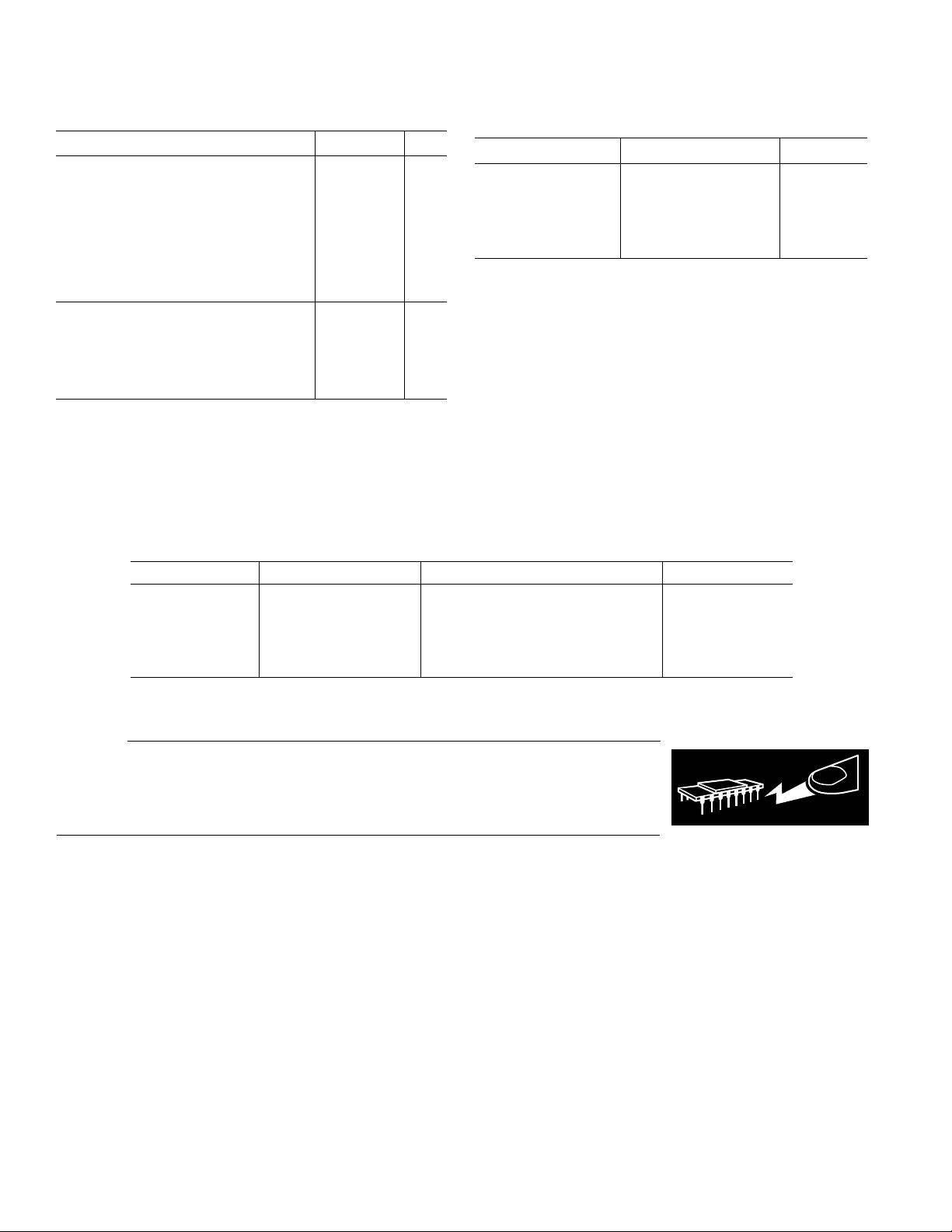
ABSOLUTE MAXIMUM RATINGS
1
Parameter Min Max Unit
ELECTRICAL
V
Voltage 0 7 V
CC
Voltage –7 0 V
V
EE
Analog Input Voltage V
EE
V
V
CC
Analog Input Current –10 +10 mA
Digital Input Voltage (ENCODE) 0 V
CC
V
ENCODE, ENCODE Differential Voltage 4 V
Digital Output Current –40 +40 mA
ENVIRONMENTAL
2
Operating Temperature (Case) –55 +125 °C
Maximum Junction Temperature 175 °C
Lead Temperature (Soldering, 10 sec) 300 °C
Storage Temperature Range (Ambient) –65 +150 °C
NOTES
1
Absolute maximum ratings are limiting values to be applied individually, and
beyond which the serviceability of the circuit may be impaired. Functional
operability is not necessarily implied. Exposure to absolute maximum rating
conditions for an extended period of time may affect device reliability.
2
Typical thermal impedances for “Z” package: θJC = 11°C/W; θJA = 30°C/W.
ORDERING GUIDE
Table I. Output Coding
MSB LSB Base 10 Input
0111111111111 2047 +FS
0000000000001 +1
0000000000000 0 0.0 V
1111111111111 –1
1000000000000 2048 –FS
EXPLANATION OF TEST LEVELS
Test Level
I – 100% Production Tested.
II – 100% production tested at 25°C, and sample tested at
specified temperatures. AC testing done on sample basis.
III – Sample Tested Only.
IV – Parameter is guaranteed by design and characterization
testing.
V – Parameter is a typical value only.
VI – All devices are 100% production tested at 25°C; sample
tested at temperature extremes.
M
odel Temperature Range Package Description Package Option
AD10242BZ –40°C to +85°C (Case) 68-Lead Ceramic Leaded Chip Carrier Z-68A
AD10242TZ –55°C to +125°C (Case) 68-
Lead
Ceramic
Leaded Chip
Carrier Z-68A
AD10242TZ/883B –55°C to +125°C (Case) 68-Lead Ceramic Leaded Chip Carrier Z-68A
5962-9581501HXA –55°C to +125°C (Case) 68-
Lead
Ceramic
Leaded Chip
Carrier Z-68A
AD10242/PCB 25°C Evaluation Board with AD10242BZ
CAUTION
ESD (electrostatic discharge) sensitive device. Electrostatic charges as high as 4000 V readily
accumulate on the human body and test equipment and can discharge without detection. Although
the AD10242 features proprietary ESD protection circuitry, permanent damage may occur on
devices subjected to high-energy electrostatic discharges. Therefore, proper ESD precautions are
recommended to avoid performance degradation or loss of functionality.
WARNING!
ESD SENSITIVE DEVICE
–4–
REV. B
AD10242
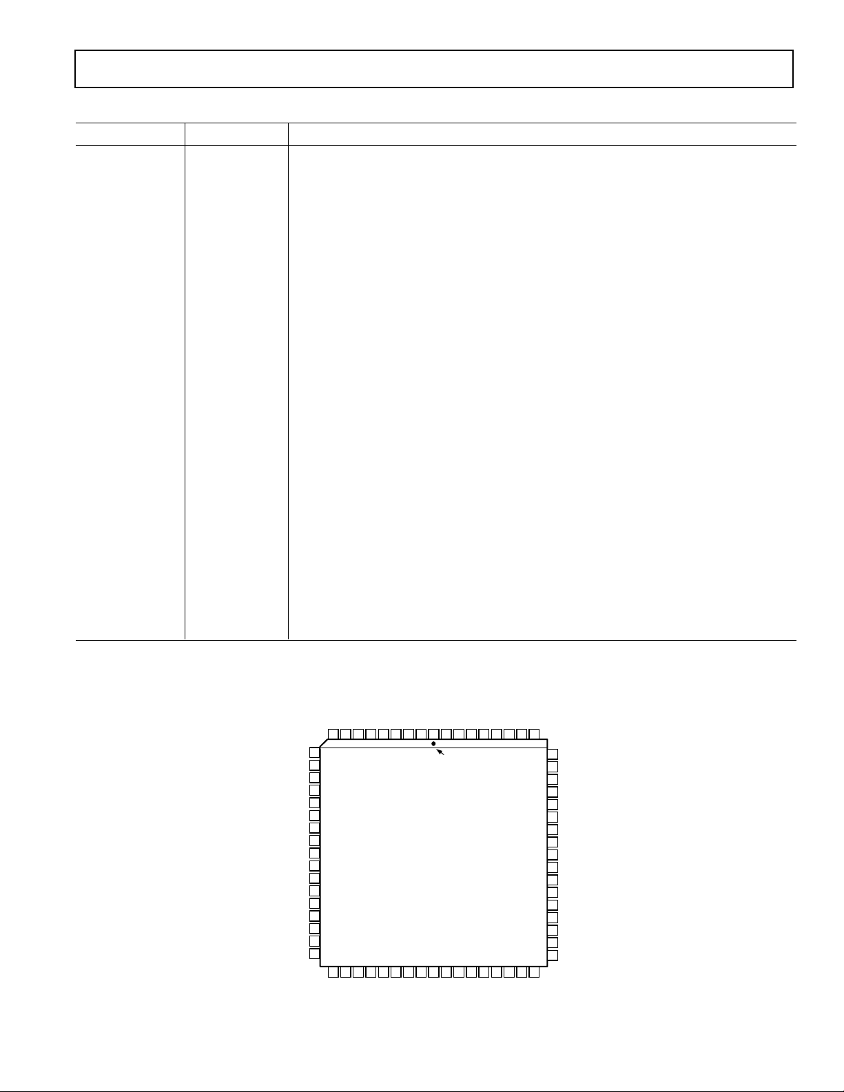
PIN FUNCTION DESCRIPTIONS
Pin No. Mnemonic Function
1 SHIELD Internal Ground Shield between Channels.
2, 5, 9–11, 26–27 GNDA A Channel Ground. A and B grounds should be connected as close to the device as possible.
3 UNEGA Unipolar Negative.
4 UCOMA Unipolar Common.
6A
7A
8A
12 UPOSA Unipolar Positive.
13 AV
14 AV
15–16 NC No Connect.
17–25, 31–33 D0A–D11A Digital Outputs for ADC A. D0 (LSB).
28 ENCODEA ENCODE is complement of ENCODE.
29 ENCODEA Data conversion initiated on rising edge of ENCODE input.
30 DV
34–35 NC No Connect.
36–42, 45–49 D0B–D11B Digital Outputs for ADC B. D0 (LSB).
43–44, 53–54 GNDB B Channel Ground. A and B grounds should be connected as close to the device
58–61, 65, 68 as possible.
50 DV
51 ENCODEB Data conversion initiated on rising edge of ENCODE input.
52 ENCODEB ENCODE is complement of ENCODE.
55 UCOMB Unipolar Common.
56 UNEGB Unipolar Negative.
57 UPOSB Unipolar Positive.
62 A
63 A
64 A
66 AV
67 AV
A1 Analog Input for A Side ADC (Nominally ± 0.5 V).
IN
A2 Analog Input for A Side ADC (Nominally ± 1.0 V).
IN
A3 Analog Input for A Side ADC (Nominally ± 2.0 V).
IN
EE
CC
CC
CC
B1 Analog Input for B Side ADC (Nominally ± 0.5 V).
IN
B2 Analog Input for B Side ADC (Nominally ± 1.0 V).
IN
B3 Analog Input for B Side ADC (Nominally ± 2.0 V).
IN
CC
EE
Analog Negative Supply Voltage (Nominally –5.0 V or –5.2 V).
Analog Positive Supply Voltage (Nominally +5.0 V).
Digital Positive Supply Voltage (Nominally +5.0 V).
Digital Positive Supply Voltage (Nominally +5.0 V).
Analog Positive Supply Voltage (Nominally +5.0 V).
Analog Negative Supply Voltage (Nominally –5.0 V or –5.2 V).
REV. B
10
GNDA
11
GNDA
12
UPOSA
13
AV
EE
14
AV
CC
15
NC
16
NC
D1A
D2A
D3A
D4A
D5A
D6A
D7A
D8A
GNDA
17
18
19
20
21
22
23
24
25
26
(LSB) D0A
NC = NO CONNECT
PIN CONFIGURATION
68-Lead Ceramic Leaded Chip Carrier
A3
A2
A1
IN
IN
IN
A
A
GNDA
UCOMA
UNEGA
GNDA
GNDA
A
9618 7 6 5 67 66 65 64 63 62432168
SHIELD
PIN 1
IDENTIFIER
GNDB
EEAVCC
AV
B3
GNDB
A
B2
B1
IN
IN
IN
A
A
GNDB
AD10242
TOP VIEW
(Not to Scale)
27 4328 29 30 31 32 33 34 35 36 37 38 39 40 41 42
GNDA
ENCODEA
CC
D9A
DV
ENCODEA
D10A
(MSB) D11A
NC
NC
(LSB) D0B
D1B
D2B
D3B
D4B
D5B
D6B
GNDB
–5–
60
GNDB
59
GNDB
58
GNDB
UPOSB
57
UNEGB
56
55
UCOMB
54
GNDB
53
GNDB
52
ENCODEB
51
ENCODEB
50
DV
49
D11B (MSB)
48
D10B
47
D9B
46
D8B
45
D7B
44
GNDB
CC

AD10242
DEFINITION OF SPECIFICATIONS
Analog Bandwidth
The analog input frequency at which the spectral power of the
fundamental frequency (as determined by the FFT analysis) is
reduced by 3 dB.
Aperture Delay
The delay between the 50% point of the rising edge of the
ENCODE command and the instant at which the analog input
is sampled.
Aperture Uncertainty (Jitter)
The sample-to-sample variation in aperture delay.
Differential Nonlinearity
The deviation of any code from an ideal 1 LSB step.
Encode Pulsewidth/Duty Cycle
Pulsewidth high is the minimum amount of time that the
ENCODE pulse should be left in Logic “1” state to achieve rated
performance; pulsewidth low is the minimum time ENCODE
pulse should be left in low state. At a given clock rate, these
Encode
specs define an acceptable
Harmonic Distortion
duty cycle.
The ratio of the rms signal amplitude to the rms value of the
worst harmonic component.
Integral Nonlinearity
The deviation of the transfer function from a reference line
measured in fractions of 1 LSB using a “best straight line” determined by a least square curve fit.
Minimum Conversion Rate
The encode rate at which the SNR of the lowest analog signal
frequency drops by no more than 3 dB below the guaranteed limit.
Maximum Conversion Rate
The encode rate at which parametric testing is performed.
Output Propagation Delay
The delay between the 50% point of the rising edge of ENCODE
command and the time when all output data bits are within
valid logic levels.
Overvoltage Recovery Time
The amount of time required for the converter to recover to
0.02% accuracy after an analog input signal of the specified
percentage of full scale is reduced to midscale.
Power Supply Rejection Ratio
The ratio of a change in input offset voltage to a change in power
supply voltage.
Signal-to-Noise-and-Distortion (SINAD)
The ratio of the rms signal amplitude (set at 1 dB below full
scale) to the rms value of the sum of all other spectral components, including harmonics but excluding dc.
Signal-to-Noise Ratio (without Harmonics)
The ratio of the rms signal amplitude (set at 1 dB below full
scale) to the rms value of the sum of all other spectral components, excluding the first five harmonics and dc.
Spurious-Free Dynamic Range
The ratio of the rms signal amplitude to the rms value of the
peak spurious spectral component. The peak spurious component may or may not be a harmonic. May be reported in dBc
(i.e., degrades as signal levels are lowered) or in dBFS (always
related back to converter full scale).
Transient Response
The time required for the converter to achieve 0.02% accuracy when a one-half full-scale step function is applied to the
analog input.
Two-Tone Intermodulation Distortion Rejection
The ratio of the rms value of either input tone to the rms value of
the worst third order intermodulation product; reported in dBc.
Two-Tone SFDR
The ratio of the rms value of either input tone to the rms value
of the peak spurious component. The peak spurious component may or may not be an IMD product. May be reported
in dBc (i.e., degrades as signal levels are lowered) or in dBFS
(always related back to converter full scale).
–6–
REV. B
AD10242
DV
CC
V
REF
DV
CC
CURRENT
MIRROR
CURRENT
MIRROR
D0 – D11
N + 1
t
= 1.0ns TYP
A
t
= 12ns TYP
OD
N – 2
N + 2 N + 3
N – 1 N N + 1 N + 2
A
ENCODE
DIGITAL
OUTPUTS
N
IN
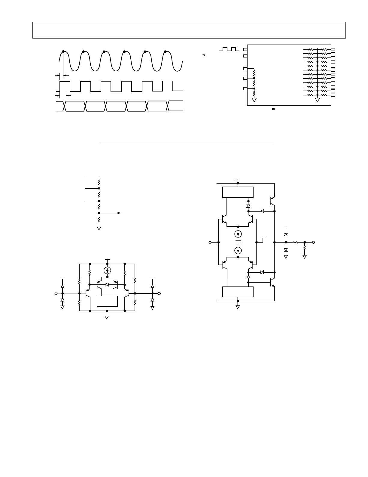
Figure 1. Timing Diagram
EQUIVALENT CIRCUITS
AIN3
A
2
IN
A
1
IN
R4
200⍀
R3
100⍀
R2
21⍀
R1
79⍀
TO AD9632
N + 4 N + 5
TTL CLOCK
f 10MHz
ENC D11
ENC
3
A
IN
2
A
IN
1
A
IN
NOTE: ALL 5V SUPPLY PINS BYPASSED
TO GND WITH A 0.1F CAPACITOR
1/2
AD10242
SHOWN
Figure 2. Equivalent Burn-In Circuit
D10
D9
D8
D7
D6
D5
D4
D3
D2
D1
D0
ENCODE
Figure 3. Analog Input Stage
AV
CC
AV
CC
17k⍀
8k⍀
R1
R2
TIMING
CIRCUITS
R1
17k⍀
R2
8k⍀
AV
CC
ENCODE
Figure 5. Digital Output Stage
Figure 4. Encode Inputs
REV. B
–7–
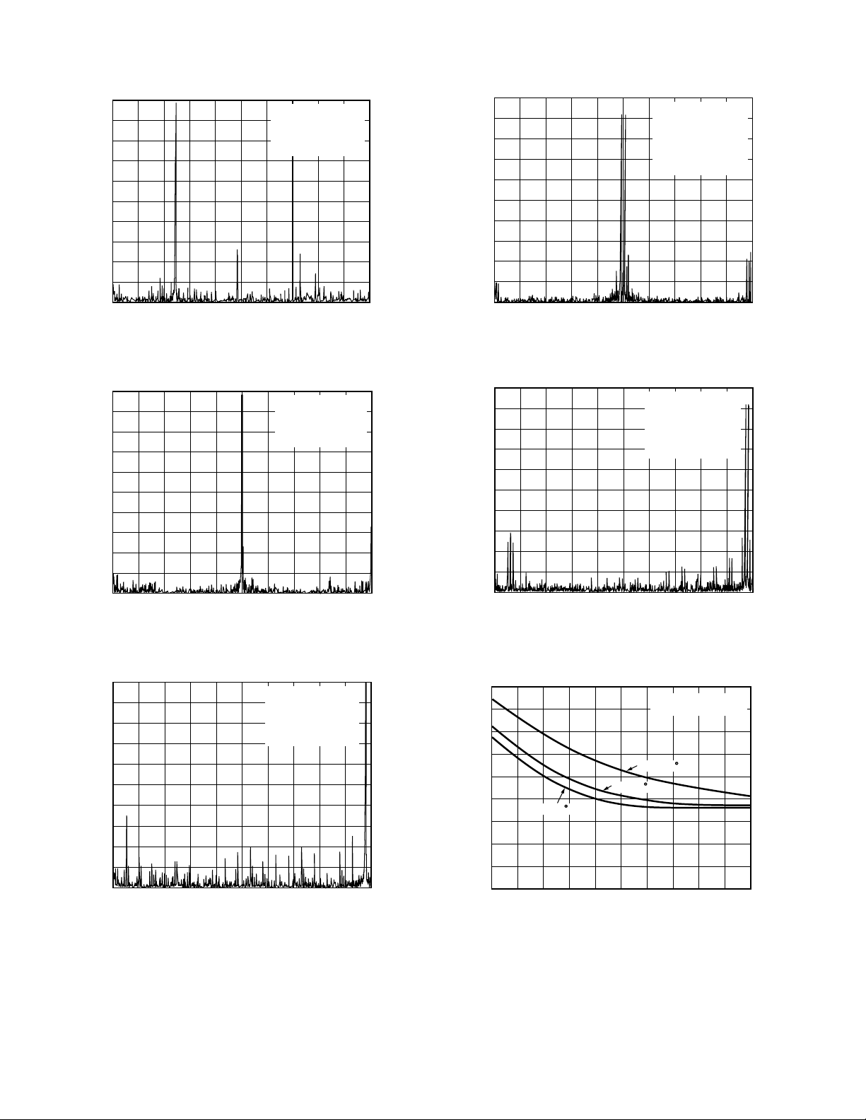
AD10242–Typical Performance Characteristics
0
–10
–20
–30
–40
–50
–60
–70
–80
POWER RELATIVE TO FULL SCALE – dB
–90
–100
02024681012141618
FREQUENCY – MHz
TPC 1. Single Tone @ 4.85 MHz
ENCODE = 40MSPS
A
= 4.85MHz
IN
= –1dBFS
A
IN
SNR = 66.4dB
SFDR = 72.8dBc
0
–10
–20
–30
–40
–50
–60
–70
–80
POWER RELATIVE TO FULL SCALE – dB
–90
–100
0202 4 6 8 1012141618
FREQUENCY – MHz
ENCODE = 40MSPS
A
1 = 9.8MHz
IN
1 = –7dBFS
A
IN
2 = 10.1MHz
A
IN
2 = –7dBFS
A
IN
SFDR = 76.0dBc
TPC 4. Two-Tone FFT @ 9.8/10.1 MHz
–10
–20
–30
–40
–50
–60
–70
–80
POWER RELATIVE TO FULL SCALE – dB
–90
–100
–10
–20
–30
–40
–50
–60
–70
–80
POWER RELATIVE TO FULL SCALE – dB
–90
–100
0
0
FREQUENCY – MHz
TPC 2. Single Tone @ 9.9 MHz
0
0
FREQUENCY – MHz
TPC 3. Single Tone @ 19.5 MHz
ENCODE = 40MSPS
A
= 9.9MHz
IN
= –1dBFS
A
IN
SNR = 66.0dB
SFDR = 65.7dBc
ENCODE = 40MSPS
= 19.5MHz
A
IN
= –1dBFS
A
IN
SNR = 64.3dB
SFDR = 63.3dBc
0
–10
–20
–30
–40
–50
–60
–70
–80
POWER RELATIVE TO FULL SCALE – dB
–90
–100
2024681012141618
02024681012141618
FREQUENCY – MHz
ENCODE = 40MSPS
1 = 19.5MHz
A
IN
1 = –7dBFS
A
IN
2 = 19.7MHz
A
IN
2 = –7dBFS
A
IN
SFDR = 70.6dBc
TPC 5. Two-Tone FFT @ 19.5/19.7 MHz
76
74
72
70
68
66
64
62
WORST-CASE HARMONIC – dB
60
2024681012141618
58
520
T = –55 C
ANALOG INPUT FREQUENCY – MHz
TPC 6. Harmonics vs. A
T = +125 C
T = +25 C
10
ENCODE = 40MSPS
= –1dBFS
A
IN
IN
–8–
REV. B

AD10242
67.0
66.5
66.0
65.5
65.0
64.5
64.0
SNR – dB
63.5
63.0
62.5
62.0
61.5
520
T = +25 C
T = +125 C
10
ANALOG INPUT FREQUENCY – MHz
TPC 7. SNR vs. A
70
68
66
64
62
SNR, WORST SPUR – dB, dBc
60
58
55010
SFDR
SNR
15 20 25 30 35 40 45
SAMPLE RATE – MSPS
T = –55 C
ENCODE = 40MSPS
= –1dBFS
A
IN
IN
AIN = 9.9MHz
AIN = –1dBFS
–90
–80
–70
–60
–50
–40
ISOLATION – dB
–30
–20
–10
0
10
90
80
70
60
50
40
30
20
WORST-CASE SPURIOUS – dBc, dBFS
10
0
–70
IN B3
15
ANALOG INPUT FREQUENCY – MHz
TPC 10. Isolation vs. Frequency
SFDR (dBc)
–60
–50 –40 –30 –20 –10 0
ANALOG INPUT POWER LEVEL – dBFS
SFDR (dBFS)
IN A1
ENCODE = 40MSPS
A
IN
25 30 35 4020
SFDR = 75dB
ENCODE = 40MSPS
A
IN B1
IN A3
= –1dBFS
= 9.98MHz
IN
TPC 8. SNR and Harmonics vs. Encode Rate
2.0
1.5
1.0
0.5
0
–0.5
ERROR IN % FS
–1.0
–1.5
–2.0
–55 125
25
TEMPERATURE – C
GAIN
OFFSET
45 65 85 1055–15–35
TPC 9. Offset and Gain Error vs. Temperature
TPC 11. Single Tone SFDR (AIN @ 9.98) vs. Power Level
100
90
80
70
60
50
40
30
20
WORST-CASE SPURIOUS – dBc, dBFS
10
0
–70
SFDR (dBFS)
SFDR (dBc)
SFDR = 75dB
ENCODE = 40MSPS
= 19.9MHz
A
IN
–60
–50 –40 –30 –20 –10 0
ANALOG INPUT POWER LEVEL – dBFS
TPC 12. Single Tone SFDR (AIN @ 19.9) vs. Power Level
REV. B
–9–
AD10242
80
70
60
50
40
30
20
SNR, WORST SPUR – dB, dBc
10
0
510
20 29.2 34.5 52.5 60.95
ANALOG INPUT FREQUENCY – MHz
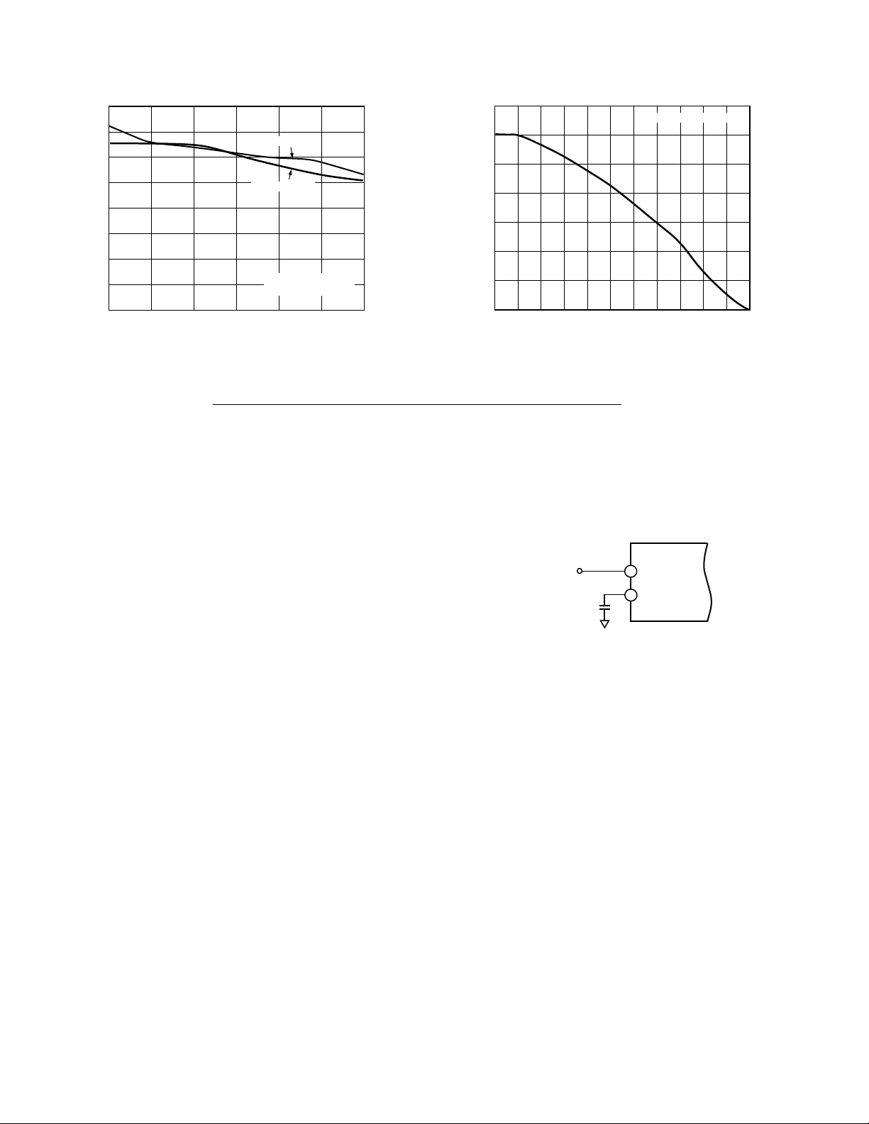
TPC 13. SNR/Harmonics to A
SNR (dB)
SFDR (dBFS)
ENCODE = 40MSPS
A
= 1dBFS
IN
> Nyquist MSPS
IN
THEORY OF OPERATION
Refer to the block diagram. The AD10242 employs three
monolithic ADI components per channel (AD9632, OP279, and
AD9042), along with multiple passive resistor networks and
decoupling capacitors to fully integrate a complete 12-bit
analog-to-digital converter.
The input signal is first passed through a precision laser trimmed
resistor divider allowing the user to externally select operation
with a full-scale signal of ±0.5 V, ±1.0 V, or ± 2.0 V by choosing
the proper input terminal for the application. The result of
the resistor divider is to apply a full-scale input of approximately
0.4 V to the noninverting input of the internal AD9632 amplifier.
The AD9632 provides the dc coupled level shift circuit required
for operation with the AD9042 ADC. Configuring the amplifier
in a noninverting mode, the ac signal gain can be trimmed to
provide a constant input to the ADC centered around the internal reference voltage of the AD9042. This allows the converter
to be used in multiple system applications without the need for
external gain and level shift circuitry normally requiring trim.
The AD9632 was chosen for its superior ac performance and
input drive capabilities, which have limited the ability of many
amplifiers to drive high-performance ADCs. As new amplifiers
are developed, pin-compatible improvements are planned to
incorporate the latest operational amplifier technology.
The OP279 provides the buffer and inversion of the internal
reference of the AD9042 in order to supply the summing node
of the AD9632 input amplifier. This dc voltage is then summed
with the input voltage and applied to the input of the AD9042
ADC. The reference voltage of the AD9042 is designed to track
internal offsets and drifts of the ADC and is used to ensure
matching over an extended temperature range of operation.
–0.5
0.5
1.0
1.5
2.0
FUNDAMENTAL LEVELS – dBFS
2.5
3.0
0
05
10 15 20 25 30 40
INPUT FREQUENCY – MHz
ENCODE = 40MSPS
45 50 5535
TPC 14. Gain Flatness vs. Input Frequency
APPLYING THE AD10242
Encoding the AD10242
The AD10242 is designed to interface with TTL and CMOS
logic families. The source used to drive the ENCODE pin(s)
must be clean and free from jitter. Sources with excessive jitter
will limit SNR and overall performance.
TTL OR CMOS
SOURCE
0.01F
AD10242
ENCODE
ENCODE
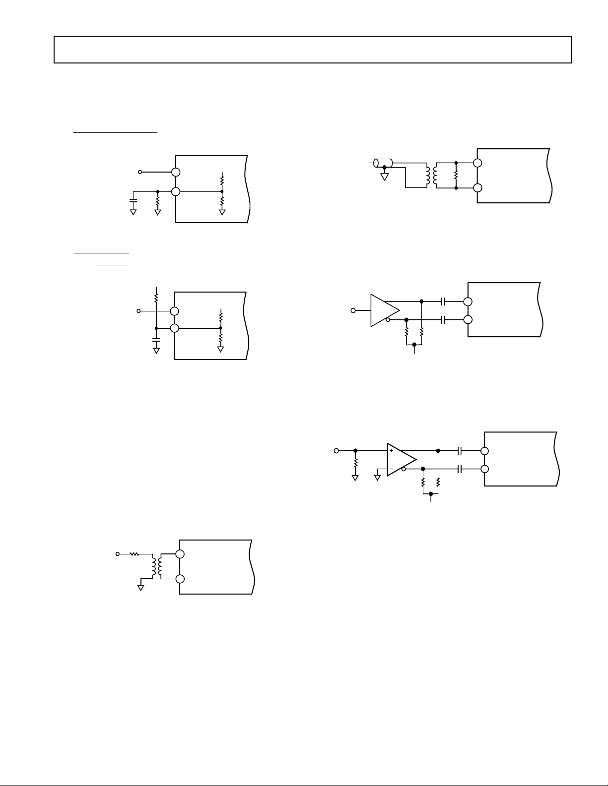
Figure 6. Single-Ended TTL/CMOS Encode
The AD10242 encode inputs are connected to a differential
input stage (see Figure 4 under Equivalent Circuits). With no
input connected to either the ENCODE or input, the voltage
divider bias the inputs to 1.6 volts. For TTL or CMOS usage,
the encode source should be connected to ENCODE (Pins 29
and/or 51). ENCODE (Pins 28 and/or 52) should be decoupled
using a low inductance or microwave chip capacitor to ground.
Devices such as AVX 05085C103MA15, a 0.01 µF capacitor,
work well.
Performance Improvements
It is possible to improve the performance of the AD10242
slightly by taking advantage of the internal characteristics of the
amplifier and converter combination. By increasing the 5 V
supply slightly, the user may be able to gain up to a 5 dB improvement in SFDR over the entire frequency range of the converter.
It is not recommended to exceed 5.5 V on the analog supplies as
there are no performance benefits beyond that range and care
should be taken to avoid the absolute maximum ratings.
–10–
REV. B
AD10242
ENCODE
ENCODE
AD10242
0.1F
0.1F
–V
S
50⍀
AD96687 (1/2)
510⍀510⍀
If a logic threshold other than the nominal 1.6 V is required,
the following equations show how to use an external resistor,
Rx, to raise or lower the trip point (see Figure 4, R1 = 17 kΩ,
R2 = 8 kΩ).
RRx
=
V
1
52
RR RRx R Rx
12 1 2
++
ENCODE
SOURCE
0.01F
R
x
to lower logic threshold.
ENCODE
V
ENCODE
l
AD10242
5V
R1
R2
Figure 7. Lower Threshold for Encode
R
V
1
52
=
R
2
RRx
1
+
RRx
1
+
ENCODE
SOURCE
to raise logic threshold.
AV
CC
R
0.01F
x
ENCODE
V
l
ENCODE
AD10242
5V
R1
R2
Figure 8. Raise Logic Threshold for Encode
While the single-ended encode will work well for many applications, driving the encode differentially will provide increased
performance. Depending on circuit layout and system noise, a
1 dB to 3 dB improvement in SNR can be realized. It is recommended that the encode signal be ac-coupled into the ENCODE
and ENCODE pins.
The simplest option is shown below. The low jitter TTL signal
is coupled with a limiting resistor, typically 100 Ω, to the primary
side of an RF transformer (these transformers are inexpensive
and readily available; part number in figure is from Mini-Circuits).
The secondary side is connected to the ENCODE and ENCODE
pins of the converter. Since both encode inputs are self-biased,
no additional components are required.
100⍀
TTL ENCODE
T1–1T
AD10242
ENCODE
If no TTL source is available, a clean sine wave may be substituted. In the case of the sine source, the matching network is
shown below. Since the matching transformer specified is a 1:1
impedance ratio, R, the load resistor should be selected to match
the source impedance. The input impedance of the AD9042
is negligible in most cases.
SINE
SOURCE
T1–1T
ENCODE
R
AD10242
ENCODE
Figure 10. Sine Source—Differential Encode
If a low jitter ECL clock is available, another option is to ac-couple
a differential ECL signal to the encode input pins as shown
below. The capacitors shown here should be chip capacitors but
do not need to be of the low inductance variety.
ECL
GATE
510⍀
0.1F
0.1F
510⍀
–V
S
ENCODE
ENCODE
AD10242
Figure 11. Differential ECL for Encode
As a final alternative, the ECL gate may be replaced by an ECL
comparator. The input to the comparator could then be a logic
signal or a sine signal.
Figure 12. ECL Comparator for Encode
Care should be taken not to overdrive the encode input pin
when ac coupled. Although the input circuitry is electrically protected from over- or undervoltage conditions, improper circuit
operations may result from overdriving the encode input pin.
REV. B
Figure 9. TTL Source—Differential Encode
–11–

AD10242
AIN2
UNEG
AD10242
2.67k⍀
UCOM
A
IN
3
A
IN
1
USING THE FLEXIBLE INPUT
The AD10242 has been designed with the user’s ease of operation in mind. Multiple input configurations have been included
on board to allow the user to have a choice of input signal levels
and input impedance. While the standard inputs are ± 0.5 V,
± 1.0 V, and ± 2.0 V, the user can select the input impedance of
the AD10242 on any input by using the other inputs as alternate
locations for GND or an external resistor. The following
chart summarizes the impedance options available at each
input location:
A
1 = 100 Ω when AIN2 and AIN3 Are Open.
IN
1 = 75 Ω when AIN3 Is Shorted to GND.
A
IN
A
1 = 50 Ω when AIN2 Is Shorted to GND.
IN
2 = 200 Ω when AIN3 Is Open.
A
IN
2 = 100 Ω when AIN3 Is Shorted to GND.
A
IN
A
2 = 75 Ω when AIN2 to AIN3 Has an External Resistor of
IN
A
2 = 300 Ω, with AIN3 Shorted to GND.
IN
2 = 50 Ω when AIN2 to AIN3 Has an External Resistor of
A
IN
A
2 = 100 Ω, with AIN3 Shorted to GND.
IN
3 = 400 Ω.
A
IN
3 = 100 Ω when AIN3 Has an External Resistor of 133 Ω to GND.
A
IN
A
3 = 75 Ω when AIN3 Has an External Resistor of 92 Ω to GND.
IN
A
3 = 50 Ω when AIN3 Has an External Resistor of 57 Ω to GND.
IN
While the analog inputs of the AD10242 are designed for dccoupled bipolar inputs, the AD10242 has the ability to use unipolar inputs in a user selectable mode through the addition of a
external resistor. This allows for 1 V, 2 V, and 4 V full-scale
unipolar signals to be applied to the various inputs (A
and A
3 respectively). Placing a 2.43 kΩ resistor (typical, off-
IN
set calibration required) between UPOS and UCOM shifts the
reference voltage setpoint to allow a unipolar positive voltage
to be applied at the inputs of the device. To calibrate offset a
midscale dc voltage should be applied to the converter while
adjusting the unipolar resistor for a midscale output transition.
AIN1
AIN2
3
A
IN
AD10242
2.43k⍀
UPOS
UCOM
Figure 13. Unipolar Positive
To operate with –1 V, –2 V, or –4 V full-scale unipolar signals
place a 2.67 kΩ resistor (typical, offset calibration required)
between UNEG and UCOM. This again shifts the reference voltage setpoint to allow a unipolar negative voltage to be applied
at the inputs of the device. To calibrate offset a midscale dc
voltage should be applied to the converter while adjusting the
unipolar resistor for a midscale output transition.
1, AIN2,
IN
Figure 14. Unipolar Negative
GROUNDING AND DECOUPLING
Analog and Digital Grounding
Proper grounding is essential in any high speed, high resolution
system. Multilayer printed circuit boards (PCBs) are recommended to provide optimal grounding and power schemes. The
use of ground and power planes offers distinct advantages:
1. The minimization of the loop area encompassed by a signal
and its return path.
2. The minimization of the impedance associated with ground
and power paths.
3. The inherent distributed capacitor formed by the power
plane, PCB insulation, and ground plane.
These characteristics result in both a reduction of electromagnetic interference (EMI) and an overall improvement in
performance.
It is important to design a layout that prevents noise from coupling to the input signal. Digital signals should not be run in
parallel with input signal traces and should be routed away from
the input circuitry. The AD10242 does not distinguish between
analog and digital ground pins as the AD10242 should always
be treated like an analog component. All ground pins should be
connected together directly under the AD10242. The PCB
should have a ground plane covering all unused portions of the
component side of the board to provide a low impedance path
and manage the power and ground currents. The ground plane
should be removed from the area near the input pins to reduce
stray capacitance.
LAYOUT INFORMATION
The schematic of the evaluation board (Figure 15) represents a
typical implementation of the AD10242. The pinout of the
AD10242 is very straightforward and facilitates ease of use
and the implementation of high frequency/high resolution
design practices. It is recommended that high quality ceramic
chip capacitors be used to decouple each supply pin to ground
directly at the device. All capacitors except the one placed on
ENCODE can be standard high quality ceramic chip capacitors.
The capacitor used on ENCODE pin must be a low inductance
chip capacitor as referenced previously in the data sheet.
–12–
REV. B

AD10242
5VA
0.1F
5VA
470⍀
470⍀
C1
K1115
R9
R10
14
V
CC
OUT
U1
V
EE
7
8
C14
0.1F
SMAJ1SMA
U5
AD9696KN
8
2
3
7
5
JA
51⍀
E5
A SECTION
PULSE A
IN
J11
49.9⍀
R3
470⍀
U3
AD8036Q
R7
3
2
SMA
VHIGH
VLOW
SMA
J2
NOTES;
1) UNIPOLAR OPERATION
A SIDE + CONNECT 2.43k⍀ RES. FROM TP1 TO TP5.
A SIDE – CONNECT 2.67k⍀ RES. FROM TP5 TO TP6.
B SIDE + CONNECT 2.43k⍀ RES. FROM TP2 TO TP4.
B SIDE – CONNECT 2.67k⍀ RES. FROM TP4 TO TP3.
2) ABOVE UNIPOLAR RESISTOR VALUES ARE
NOMINAL AND MAY HAVE TO BE ADJUSTED
DEPENDING ON OFFSET OF DUT.
3) ENCODE SOURCES
A)FOR NORMAL OPERATION, A 40MHz TTL CLOCK
OSCILLATOR IS INSTALLED IN U1 AND U2. THERE
IS A 51⍀ RESISTOR BETWEEN J15 AND J16.
J17 AND J18 ARE OPEN.
B)FOR EXTERNAL SQUARE WAVE ENCODE, INPUT
SIGNAL AT J1 AND J8, REMOVE U1, U2, JUMPERS
J15 AND J16. CONNECT JUMPERS J17 AND J18.
C)FOR EXTERNAL SINE WAVE ENCODE, INPUT
SIGNAL AT J1 AND J8, REMOVE U1, U2, R9, R11,
JUMPERS J15 AND J16.
CONNECT JUMPERS J17 AND J18.
4) POWER (5VD) FOR DIGITAL OUTPUTS OF THE
AD10242 IS SUPPLIED VIA PIN 1 OF EITHER J9 OR J10
(THE DIGITAL INTERFACES). TO POWER THE EVAL.
BOARD WITH ONE 5V SUPPLY, JUMPER A WIRE
FROM E1 TO E4 (CONNECTED AT FACTORY).
SMA
J3
A1
A
IN
VHIGH
8
5
VLOW
R5
470⍀
A
IN
A2
PULSE A
6
U4
C22
0.1F
U3
C19
0.1F
SMA
J4
OUT
SMA
J12
A
U3
C21
0.1F
U4
C20
0.1µF
IN
PULSE B
SMA
J5
A3
H2DM
J15
12
H2DM
J17
12
R1
100⍀
IN
SMA
J13
49.9⍀
R4
470⍀
+5V
–5.2V
B1
A
IN
GND
U4
AD8036Q
R8
U4
C17
0.1F
U3
C15
0.1F
SMA
J6
GND
GND
TP1
–5.2V
+5VA
GND
GND
D0A
D1A
D2A
D3A
D4A
D5A
D6A
D7A
D8A
GND
SMA
JC
BUFLATA
T1
T1–1T
3
2
1
1 : 1
VHIGH
3
2
VLOW
R6
470⍀
U3
C18
0.1F
U4
C16
0.1F
B2
A
IN
10
GNDA
11
GNDA
12
UNIPOSA
13
–5.2VAA
14
+5VAA
15
NCA
16
NCA
17
D0A (LSBA)
18
D1A
19
D2A
20
D3A
21
D4A
22
D5A
23
D6A
24
D7A
25
D8A
26
GNDA
5VA
C2
K1115
14
U2
0.1F
5VA
R11
470⍀
R12
4
6
8
ENCAB
ENCA
PULSE B
6
OUT
SMA
J14
470⍀
+5VA
5
–5.2V
DUT
C9
0.1F
C24
10F
+5VD
SMA
J7
B3
A
IN
A3
A1
A2
IN
IN
IN
A
GND
9618765 686766656463624321
GNDA
A3
A
GND
A
A
A1
A2
IN
IN
IN
GNDA
A
A
C23
10F
DUT
C10
0.1F
TP5
TP6
UNINEGA
UNICOMA
GND
GND
GNDA
SHIELD
U5
C12
0.1F
U5
C13
0.1F
DUT
C7
0.1F
GND
GNDB
–5.2V
+5VA
+5VAB
–5.2VAB
DUT
AD10242
GNDA
ENCA
ENCA
+5VDA
D9A
NCB
NCB
D0B (LSBB)
D1B
GND
D0B
D1B
D2B
D2B
D10A
+5VD
D9A
D10A
D11A (MSBA)
GND
D11A
27 4328 29 30 31 32 33 34 35 36 37 38 39 40 41 42
GND
ENCA
ENCA
V
CC
8
OUT
V
EE
7
AD9696KN
2
3
C5
0.1F
B SECTION
B JACKS
E1
+5VA
GND
E2
VLOW VLOW
VHIGH
–5.2V
DUT
U6
C8
C3
0.1F
0.1F
DUT
U6
C11
C4
0.1F
0.1F
DUT
C25
C6
10F
0.1F
B2
B1
B3
IN
IN
IN
A
A
A
GND
B2
B1
B3
IN
IN
IN
GNDB
A
A
A
UNIPOSB
UNINEGB
UNICOMB
(MSBB) D11B
D3B
D4B
D5B
D6B
D3B
D4B
D5B
D6B
SMAJ8SMA
JB
U5
8
7
5
GND
GNDB
GNDB
GNDB
GNDB
GNDB
GNDB
ENCB
ENCB
+5VDB
D10B
D9B
D8B
D7B
GNDB
GNDB
GND
51⍀
E5
E3
GND
VHIGH
60
GND
59
GND
58
GND
57
TP2
56
TP3
55
TP4
54
GND
53
GND
52
ENCB
51
ENCB
50
+5VD
49
D11B
48
D10B
47
D9B
46
D8B
45
D7B
44
GND
H2DM
J16
12
H2DM
J18
12
R2
100⍀
BUFLATB
GND
5VD
(MSB) D11A
BUFLATA
(LSB) D0A
(MSB) D11B
(LSB) D0B
TP1 TP1
TP2 TP2
TP3 TP3
TP4 TP4
TP5 TP5
SMA
JD
BUFLATB
T2
T1–1T
4
3
ENCBB
2
1
6
ENCB
1 : 1
H40DM
E4
J9
140
239
338
D10A
437
D9A
536
D8A
635
D7A
734
D6A
833
D5A
932
D4A
10 31
11
12 29
D3A
128
13
D2A
14 27
D1A
15 26
16 25
GND
17 24
GND
18 23
GND
19 22
GND
20 21
GND
H40DM
J10
140
+5VD
239
338
D10B
437
D9B
536
D8B
635
D7B
734
D6B
833
D5B
932
D4B
10 31
11
12 29
D3B
13
D2B
14
D1B
15 26
16 25
GND
17 24
GND
18 23
GND
19 22
GND
20 21
GND
TEST POINTS
TP6
TP7
TP8
TP9
TP10
30
30
28
27
TP6
ENCAB
ENCA
ENCBB
ENCB
GND
GND
GND
GND
GND
GND
GND
GND
GND
GND
GND
GND
GND
GND
GND
GND
GND
GND
GND
GND
GND
GND
GND
GND
GND
GND
GND
GND
GND
GND
GND
GND
GND
GND
GND
GND
GND
GND
GND
GND
REV. B
Figure 15. Evaluation Board Schematic
–13–

AD10242
Care should be taken when placing the digital output runs.
Because the digital outputs have such a high slew rate, the
capacitive loading on the digital outputs should be minimized.
Circuit traces for the digital outputs should be kept short and
connect directly to the receiving gate. Internal circuitry buffers
the outputs of the AD9042 ADC through a resistor network to
eliminate the need to externally isolate the device from the
receiving gate.
EVALUATION BOARD
The AD10242 evaluation board (see Figure 16) is designed to
provide optimal performance for evaluation of the AD10242
analog-to-digital converter. The board encompasses everything
needed to ensure the highest level of performance for evaluating
the AD10242.
Power to the analog supply pins is connected via banana jacks.
The analog supply powers the crystal oscillator, the associated
components and amplifiers, and the analog section of the
AD10242. The digital outputs of the AD10242 are powered via
Pin 1 of either J9 or J10 found on the digital interface connector. To power the evaluation board with one 5 V supply, a
jumper wire is required from test point E1 to E4. Contact the
factory if additional layout or applications assistance is required.
Figure 16. Evaluation Board Mechanical Layout
–14–
REV. B
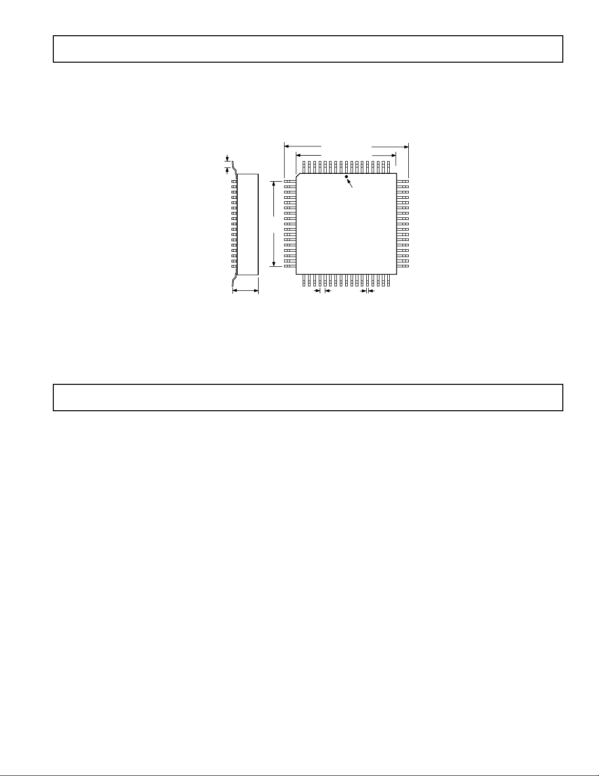
OUTLINE DIMENSIONS
Dimensions shown in inches and (mm).
68-Lead Ceramic Leaded Chip Carrier
(Z-68A)
1.180 (29.97) SQ
0.060
(1.52)
10
0.950 (24.13) SQ
9
PIN 1
AD10242
61
60
0.240 (6.096)
Location
Data Sheet changed from REV. A to REV. B.
AD9631 references changed to AD9632.
0.800
(20.32)
TOP VIEW
(PINS DOWN)
26
0.050 (1.27) 0.018 (0.457)
44
4327
Revision History–AD10242
REV. B
–15–

C00665a–0–6/01(B)
–16–
PRINTED IN U.S.A.
 Loading...