Analog Devices AD10201 Datasheet

Dual-Channel, 12-Bit 105 MSPS
a
FEATURES
Two Independent 12-Bit, 105 MSPS ADCs
Channel-to-Channel Isolation, > 90 dB
AC-Coupled Signal Conditioning Included
Gain Flatness up to Nyquist, < 0.1 dB
Input VSWR 1.05:1 to Nyquist
80 dB Spurious-Free Dynamic Range
Two’s Complement Output Format
3.3 V or 5 V CMOS-Compatible Output Levels
900 mW Per Channel
Single-Ended or Differential Input
250 MHz Input Bandwidth
APPLICATIONS
Wireless and Wired Broadband Communications
Base Stations and “Zero-IF” or Direct IF Sampling
Subsystems
Wireless Local Loop (WLL)
Local Multipoint Distribution Service (LMDS)
Radar and Satellite Subsystems
IF Sampling A/D Converter
AD10201
PRODUCT DESCRIPTION
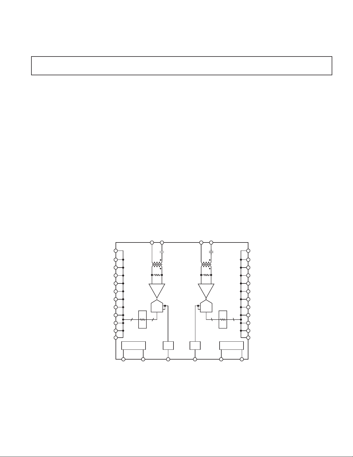
The AD10201 offers two complete ADC channels with on-module
signal conditioning for improved dynamic performance. Each wide
dynamic range ADC has a transformer coupled front end optimized
for direct IF sampling. The AD10201 has on-chip track-and-hold
circuitry, and uses an innovative architecture to achieve 12-bit,
105 MSPS performance. The AD10201 uses innovative high
density circuit design to achieve exceptional performance while still
maintaining excellent isolation and providing for board area savings.
The AD10201 operates with 5.0 V supply for the analog-to-digital
conversion. Each channel is completely independent, allowing
operation with independent ENCODE and analog inputs. The
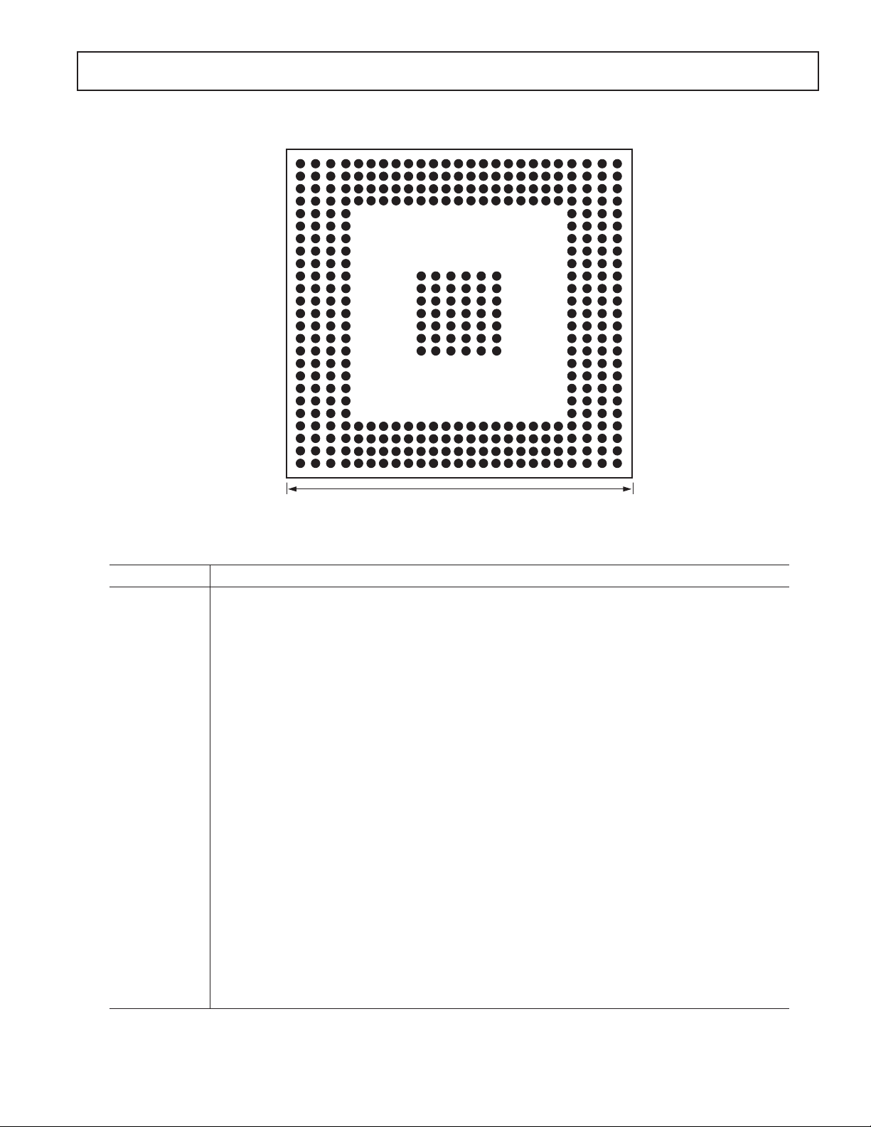
AD10201 is available as a 35 mm square 385-lead BGA package.
PRODUCT HIGHLIGHTS
1. Guaranteed sample rate of 105 MSPS
2. Input signal conditioning included with full-power bandwidth
to 250 MHz
3. Industry-leading IF sampling performance
D0A
(LSB)
D1A
D2A
D3A
D4A
D5A
D6A
D7A
D8A
D9A
D10A
D11A
(MSB)
TIMING
ENCODEA
FUNCTIONAL BLOCK DIAGRAM
AINA2
A1 AINB1
A
IN
T1A
12
OUTPUT
RESISTORS
ENCODEA
50⍀
T/H T/H
AD10201
ADC
12
REF
REF_A_OUT
REF_B_OUT
50⍀
ADC
REF
AINB2
T1B
12 12
OUTPUT
RESISTORS
ENCODEB
TIMING
ENCODEB
D0B
(LSB)
D1B
D2B
D3B
D4B
D5B
D6B
D7B
D8B
D9B
D10B
D11B
(MSB)
REV. 0
Information furnished by Analog Devices is believed to be accurate and
reliable. However, no responsibility is assumed by Analog Devices for its
use, nor for any infringements of patents or other rights of third parties that
may result from its use. No license is granted by implication or otherwise
under any patent or patent rights of Analog Devices.
One Technology Way, P.O. Box 9106, Norwood, MA 02062-9106, U.S.A.
Tel: 781/329-4700www.analog.com
Fax: 781/326-8703 © Analog Devices, Inc., 2002

AD10201–SPECIFICATIONS
1
(V
ELECTRICAL CHARACTERISTICS
= 3.3 V, V
DD
Parameter Temp Level Min Typ Max Unit
RESOLUTION 12 Bits
DC ACCURACY
Differential Nonlinearity Full IV –0.99 ±0.5 +0.99 LSB
Integral Nonlinearity Full IV ±1.5 ± 0.1 +1.5 LSB
No Missing Codes Full IV Guaranteed
Gain Error
2
25°CI –9 ± 2+9% FS
Output Offset 25°CI –8 ± 2+8LSB
Gain Tempco Full V 60 ppm/°C
Offset Tempco Full V –12 ppm/°C
ANALOG INPUT
Input Voltage Range 25°CV 1.75 V p-p
Input Impedance 25°CV 50 Ω
Input VSWR
3
Full V 1.05:1 Ratio
Analog Input Bandwidth, High Full V 250 MHz
Analog Input Bandwidth, Low Full V 300 kHz
ANALOG REFERENCE
Output Voltage 25°CV 2.5 V
Load Current 25°CV 5 mA
Tempco Full V 50 ppm/°C
SWITCHING PERFORMANCE
4
Maximum Conversion Rate Full VI 105 MSPS
Minimum Conversion Rate Full IV 10 MSPS
Duty Cycle Full IV 45 50 55 %
Aperture Delay (t
Aperture Uncertainty (Jitter) 25°CV 0.25 ps rms
Output Valid Time (t
Output Propagation Delay (t
Output Rise Time (t
)25°CV 2.0 ns
A
5
)
V
)25°CV 3.5 ns
R
PD
5
)
Full IV 3.0 6.3 ns
Full IV 6.5 9.0 ns
Output Fall Time (tF)25°CV 3.3 ns
DIGITAL INPUTS
ENCODE Input Common-Mode Full IV 1.2 1.6 2.0 V
Differential Input (ENC, ENC) Full IV 0.4 5.0 V
Logic “1” Voltage Full IV 2.0 V
Logic “0” Voltage Full IV 0.8 V
Input Resistance Full IV 3 5 8.0 kΩ
Input Capacitance 25°CV 4.5 pF
DIGITAL OUTPUTS
Logic “1” Voltage
Logic “0” Voltage
5
5
Full IV 3.1 3.3 V
Full IV 0 0.2 V
Output Coding Two’s Complement
POWER SUPPLY
Power Dissipation
6
7
Full VI 1800 2200 mW
Power Supply Rejection Ratio Full IV –5.0 ±0.5 +5.0 mV/V
Total I (DV
) Current Full VI 32 40 mA
DD
Total I (AVCC) Current Full VI 340 410 mA
= 5.0 V; ENCODE = 105 MSPS, unless otherwise noted.)
CC
Test
–2–
REV. 0

AD10201
Test
Parameter Temp Level Min Typ Max Unit
DYNAMIC PERFORMANCE
Signal-to-Noise Ratio (SNR)8 (Without Harmonics)
f
= 10 MHz 25°CI 66 68 dBFS
IN
f
= 41 MHz 25°CV 67 dBFS
IN
= 71 MHz 25°CI 63.5 66.5 dBFS
f
IN
f
= 121 MHz 25°CV 63 dBFS
IN
Signal-to-Noise Ratio (SINAD)
f
= 10 MHz 25°CI 65.5 67.5 dBFS
IN
= 41 MHz 25°CV 67.2 dBFS
f
IN
f
= 71 MHz 25°CI 63 65 dBFS
IN
f
= 121 MHz 25°CV 59 dBFS
IN
Spurious-Free Dynamic Range
fIN = 10 MHz 25°CI 75.5 81 dBFS
f
= 41 MHz 25°CV 76 dBFS
IN
f
= 71 MHz 25°CI 71 74 dBFS
IN
= 121 MHz 25°CV 63 dBFS
f
IN
Two-Tone Intermodulation
Distortion
f
IN
f
IN
f
IN
11
(IMD)
= 10 MHz; fIN = 12 MHz 25°CV 81 dBc
= 71 MHz; fIN = 72 MHz 25°CV 66 dBc
= 121 MHz; fIN = 122 MHz 25°CV 61 dBc
Channel-to-Channel Isolation
fIN = 121 MHz Full IV 90 dBc
9
(With Harmonics)
10
12
NOTES
1
All specifications tested by driving ENCODE and ENCODE differentially, with the analog input applied to AINX1 and AINX2 tied to ground.
2
Gain error measured at 10.3 MHz.
3
Input VSWR, see TPC 12.
4
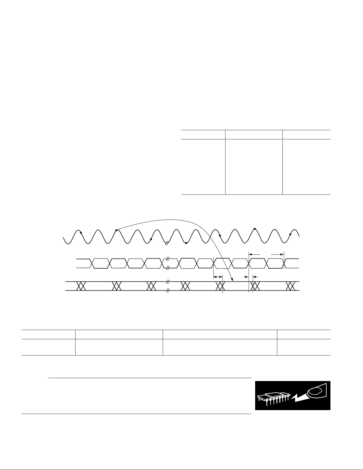
See Figure 1, Timing Diagram.
5
tV and tPD are measured from the transition points of the ENCODE input to the 50%/50% levels of the digital outputs swing. The digital output load during test is
not to exceed an ac load of 10 pF or a dc current of ± 40 A.
6
Supply voltages should remain stable within ± 5% for normal operation.
7
Power dissipation measures with encode at rated speed.
8
Analog input signal power at –1 dBFS; signal-to-noise (SNR) is the ratio of signal level to total noise (first six harmonics removed).
ENCODE = 105 MSPS. SNR is reported in dBFS, related back to converter full scale.
9
Analog input signal power at –1 dBFS; signal-to-noise and distortion (SINAD) is the ratio of signal level to total noise + harmonics. ENCODE = 105 MSPS.
SINAD is reported in dBFS, related back to converter full scale.
10
Analog input signal equals –1 dBFS; SFDR is ratio of converter full scale to worst spur.
11
Both input tones at –7 dBFS; two-tone intermodulation distortion (IMD) rejection is the ratio of either tone to the worst third order intermod product.
12
Channel-to-channel isolation tested with A channel/50 Ω terminated (AINA2 grounded) and a full-scale signal applied to B channel (AINB2).
Specifications subject to change without notice.
REV. 0
–3–

AD10201
WARNING!
ESD SENSITIVE DEVICE
ABSOLUTE MAXIMUM RATINGS*
VDD . . . . . . . . . . . . . . . . . . . . . . . . . . . . . . . . . . . . . . . . . . 6 V
V
. . . . . . . . . . . . . . . . . . . . . . . . . . . . . . . . . . . . . . . . . . 6 V
CC
Analog Inputs . . . . . . . . . . . . . . . . . . . . . . 5 V p-p (18 dBm)
Digital Inputs . . . . . . . . . . . . . . . . . . . . –0.5 V to V
+0.5 V
DD
Digital Output Current . . . . . . . . . . . . . . . . . . . . . . . . 20 mA
Operating Temperature (Ambient) . . . . . . . –55°C to +125°C
Storage Temperature (Ambient) . . . . . . . . . –65°C to +150°C
Maximum Junction Temperature . . . . . . . . . . . . . . . . . 150°C
* Stresses above those listed under Absolute Maximum Ratings may cause permanent
damage to the device. This is a stress rating only; functional operation of the device
at these or any other conditions outside of those indicated in the operation sections
of this specification is not implied. Exposure to absolute maximum ratings for
extended periods may affect device reliability.
THERMAL CHARACTERISTICS
385-Lead BGA Package:
The typical θ
of the module as determined by an IR scan is
JA
25.33°C/W.
EXPLANATION OF TEST LEVELS
Test Level
I 100% production tested
II 100% production tested at 25°C and sample tested at specific
temperatures
III Sample tested only
IV Parameter is guaranteed by design and characterization
testing
V Parameter is a typical value only
VI 100% production tested at 25°C; guaranteed by design and
characterization testing for industrial temperature range
Table I. Output Coding (V
= 2.5 V) (Two’s Complement)
REF
Code AIN (V) Digital Output
+2047 +0.875 0111 1111 1111
·· ·
·· ·
00 0000 0000 0000
–1 –0.000427 1111 1111 1111
·· ·
·· ·
–2048 –0.875 1000 0000 0000
SAMPLE Nⴚ1SAMPLE N SAMPLE Nⴙ10 SAMPLE Nⴙ11
AIN
SAMPLE Nⴙ9SAMPLE Nⴙ1
1/f
ENCODE
ENCODE
D11ⴚD0
t
PD
DATA Nⴚ11 DATA Nⴚ10 Nⴚ9 DATA Nⴚ1 DATA N DATA N ⴙ 1
Nⴚ2
S
t
V
Figure 1. Timing Diagram
ORDERING GUIDE
Model Temperature Range Package Description Package Option
AD10201AB –25°C to +85°C (Ambient) 385-Lead BGA (35 mm 35 mm) B-385
AD10201/PCB +25°CEvaluation Board with AD10201AB
CAUTION
ESD (electrostatic discharge) sensitive device. Electrostatic charges as high as 4000 V readily
accumulate on the human body and test equipment and can discharge without detection. Although
the AD10201 features proprietary ESD protection circuitry, permanent damage may occur on
devices subjected to high-energy electrostatic discharges. Therefore, proper ESD precautions are
recommended to avoid performance degradation or loss of functionality.
–4–
REV. 0

PIN CONFIGURATION
25 23 21 19 17 15 13 11 9 7 5 3 1
24 22 20 18 16 14 12 10 8 6 4 2
A
B
C
D
E
F
G
H
J
K
L
M
N
P
R
T
U
V
W
Y
AA
AB
AC
AD
AE
AD10201
35 mm square
BOTTOM VIEW
PIN FUNCTION DESCRIPTIONS
Mnemonic Function
AGNDA A Channel Analog Ground. A and B grounds should be connected as close to the device as possible
REF_A_OUT A Channel Internal Voltage Reference
NC No connection
A1 Analog Input for A side ADC (ⴚ input)
A
IN
A2 Analog Input for A side ADC (+ input)
A
IN
AAnalog Positive Supply Voltage (nominally 5.0 V)
AV
CC
DGNDA A Channel Digital Ground
D11A–D0A Digital Outputs for ADC A. D0 (LSB)
ENCODEA Complement of ENCODE
ENCODEA Data conversion initiated on the rising edge of ENCODE input
ADigital Positive Supply Voltage (nominally 3.3 V)
DV
CC
DGNDB B Channel Digital Ground
D11B–D0B Digital Outputs for ADC B. D0 (LSB)
AGNDB B Channel Analog Ground. A and B grounds should be connected as close to the device as possible.
BDigital Positive Supply Voltage (nominally 3.3 V)
DV
CC
ENCODEB Complement of ENCODE
ENCODEB Data conversion initiated on rising edge of ENCODE input
REF_B_OUT B Channel Internal Voltage Reference
B1 Analog Input for B side ADC (ⴚ input)
A
IN
B2 Analog Input for B side ADC (+ input)
A
IN
AVCCBAnalog Positive Supply Voltage (nominally 5.0 V)
REV. 0
–5–

AD10201
385-LEAD BGA PINOUT
Ball Signal Ball Signal Ball Signal Ball Signal Ball Signal Ball Signal
No. Name No. Name No. Name No. Name No. Name No. Name
A1 AGNDA
A2 AGNDA
A3 AGNDA
A4 AGNDA
A5 AGNDA
A6 AGNDA
A7 DNC
A8 DNC
A9 AGNDA
A10 AV
CC
A
A11 REF_A_OUT
A12 AGNDA
A13 DNC
A14 AGNDB
A15 AGNDB
A16 AV
CC
B
A17 AGNDB
A18 AV
CC
B
A19 DNC
A20 DNC
A21 AGNDB
A22 AGNDB
A23 AGNDB
A24 AGNDB
A25 AGNDB
B1 AGNDA
B2 AGNDA
B3 AGNDA
B4 AGNDA
B5 AGNDA
B6 AGNDA
B7 DNC
B8 DNC
B9 AGNDA
B10 AV
CC
A
B11 REF_A_OUT
B12 AGNDA
B13 DNC
B14 AGNDB
B15 AGNDB
B16 AV
CC
B
B17 AGNDB
B18 AV
CC
B
B19 DNC
B20 DNC
B21 AGNDB
B22 AGNDB
B23 AGNDB
B24 AGNDB
B25 AGNDB
C1 AGNDA
C2 AGNDA
C3 AGNDA
C4 AGNDA
C5 AGNDA
C6 AGNDA
C7 DNC
C8 DNC
C9 AGNDA
C10 AV
CC
A
C11 REF_A_OUT
C12 AGNDA
C13 DNC
C14 AGNDB
C15 AGNDB
C16 AV
CC
B
C17 AGNDB
C18 AV
CC
B
C19 DNC
C20 DNC
C21 AGNDB
C22 AGNDB
C23 AGNDB
C24 AGNDB
C25 AGNDB
D1 AGNDA
D2 AGNDA
D3 AGNDA
D4 AGNDA
D5 AGNDA
D6 AGNDA
D7 A
D8 A
A2
IN
A1
IN
D9 AGNDA
D10 AV
CC
A
D11 REF_A_OUT
D12 AGNDA
D13 DNC
D14 AGNDB
D15 AGNDB
D16 AV
CC
B
D17 AGNDB
D18 AV
D19 A
D20 A
B
CC
B2
IN
B1
IN
D21 AGNDB
D22 AGNDB
D23 AGNDB
D24 AGNDB
D25 AGNDB
E1 AGNDA
E2 AGNDA
E3 AGNDA
E4 AGNDA
E22 AGNDB
E23 AGNDB
E24 AGNDB
E25 AGNDB
F1 AGNDA
F2 AGNDA
F3 AGNDA
F4 AGNDA
F22 AGNDB
F23 AGNDB
F24 AGNDB
F25 AGNDB
G1 AGNDA
G2 AGNDA
G3 AGNDA
G4 AGNDA
G22 AGNDB
G23 AGNDB
G24 AGNDB
G25 AGNDB
H1 AGNDA
H2 AGNDA
H3 AGNDA
H4 AGNDA
H22 AGNDB
H23 AGNDB
H24 AGNDB
H25 AGNDB
J1 AV
J2 AV
J3 AV
J4 AV
CC
CC
CC
CC
A
A
A
A
J22 REF_B_OUT
J23 REF_B_OUT
J24 REF_B_OUT
J25 REF_B_OUT
K1 AGNDA
K2 AGNDA
K3 AGNDA
K4 AGNDA
K10 AV
CC
A
K11 AGNDA
K12 AGNDA
K13 DNC
K14 AGNDB
K15 AGNDB
K16 AV
CC
B
K22 AGNDB
K23 AGNDB
K24 AGNDB
K25 AGNDB
L1 AGNDA
L2 AGNDA
L3 AGNDA
L4 AGNDA
L10 DNC
L11 AGNDA
L12 AGNDA
L13 DNC
L14 AGNDB
L15 AGNDB
L16 DNC
L22 ENCBB
L23 ENCBB
L24 ENCBB
L25 ENCBB
M1 ENCAB
M2 ENCAB
M3 ENCAB
M4 ENCAB
M10 AGNDA
M11 AGNDA
M12 AGNDA
M13 DNC
M14 AGNDB
M15 AGNDB
M16 AGNDB
M22 ENCB
M23 ENCB
M24 ENCB
M25 ENCB
N1 ENCA
N2 ENCA
N3 ENCA
N4 ENCA
N10 AGNDA
N11 AGNDA
N12 AGNDA
N13 DNC
N14 AGNDB
N15 AGNDB
N16 AGNDB
N22 AGNDB
N23 AGNDB
N24 AGNDB
N25 AGNDB
P1 AGNDA
P2 AGNDA
P3 AGNDA
P4 AGNDA
P10 AGNDA
P11 AGNDA
P12 AGNDA
P13 DNC
P14 AGNDB
P15 AGNDB
P16 AGNDB
P22 DV
P23 DV
P24 DV
P25 DV
P25 DV
R1 DV
R2 DV
R3 DV
R4 DV
CC
CC
CC
CC
CC
CC
CC
CC
CC
B
B
B
B
B
A
A
A
A
R10 AGNDA
R11 AGNDA
R12 AGNDA
R13 DNC
R14 AGNDB
R15 AGNDB
R16 AGNDB
R22 DB0
R23 DB0
R24 DB0
R25 DB0
T1 DA11
T2 DA11
T3 DA11
T4 DA11
T10 AV
CC
A
T11 AGNDA
T12 AGNDA
T13 DNC
T14 AV
CC
B
T15 AGNDB
T16 AGNDB
T22 DB1
T23 DB1
T24 DB1
T25 DB1
U1 DA10
U2 DA10
U3 DA10
U4 DA10
U22 DB2
U23 DB2
U24 DB2
U25 DB2
V1 DA9
V2 DA9
V3 DA9
V4 DA9
V22 DB3
V23 DB3
V24 DB3
V25 DB3
W1 DA8
W2 DA8
W3 DA8
W4 DA8
W22 DB4
W23 DB4
W24 DB4
W25 DB4
Y1 DA7
Y2 DA7
Y3 DA7
Y4 DA7
Y22 DB5
Y23 DB5
Y24 DB5
Y25 DB5
AA1 DGNDA
AA2 DGNDA
AA3 DGNDA
AA4 DGNDA
AA22 DGNDB
AA23 DGNDB
AA24 DGNDB
AA25 DGNDB
AB1 OVRA
AB2 OVRA
AB3 OVRA
AB4 OVRA
AB5 DGNDA
AB6 DA6
AB7 DA5
AB8 DA4
AB9 DA3
AB10 DA2
AB11 DA1
AB12 DA0
AB13 DGNDA
AB14 DGNDB
AB15 DB11
AB16 DB10
AB17 DB9
AB18 DB8
AB19 DB7
AB20 DB6
AB21 DGNDB
AB22 OVRB
AB23 OVRB
AB24 OVRB
AB25 OVRB
AC1 DGNDA
AC2 DGNDA
AC3 DGNDA
AC4 DGNDA
AC5 DGNDA
AC6 DA6
AC7 DA5
AC8 DA4
AC9 DA3
AC10 DA2
AC11 DA1
AC12 DA0
AC13 DGNDA
AC14 DGNDB
AC15 DB11
AC16 DB10
AC17 DB9
AC18 DB8
AC19 DB7
AC20 DB6
AC21 DGNDB
AC22 DGNDB
AC23 DGNDB
AC24 DGNDB
AC25 DGNDB
AD1 DGNDA
AD2 DGNDA
AD3 DGNDA
AD4 DGNDA
AD5 DGNDA
AD6 DA6
AD7 DA5
AD8 DA4
AD9 DA3
AD10 DA2
AD11 DA1
AD12 DA0
AD13 DGNDA
AD14 DGNDB
AD15 DB11
AD16 DB10
AD17 DB9
AD18 DB8
AD19 DB7
AD20 DB6
AD21 DGNDB
AD22 DGNDB
AD23 DGNDB
AD24 DGNDB
AD25 DGNDB
AE1 DGNDA
AE2 DGNDA
AE3 DGNDA
AE4 DGNDA
AE5 DGNDA
AE6 DA6
AE7 DA5
AE8 DA4
AE9 DA3
AE10 DA2
AE11 DA1
AE12 DA0
AE13 DGNDA
AE14 DGNDB
AE15 DB11
AE16 DB10
AE17 DB9
AE18 DB8
AE19 DB7
AE20 DB6
AE21 DGNDB
AE22 DGNDB
AE23 DGNDB
AE24 DGNDB
AE25 DGNDB
–6–
REV. 0
 Loading...