Dual Channel, 12-Bit 105 MSPS IF Sampling
A/D Converter with Analog Input
a
FEATURES
Dual, 105 MSPS Minimum Sample Rate
Channel-Channel Isolation, >80 dB
AC-Coupled Signal Conditioning Included
Gain Flatness up to Nyquist: < 0.2 dB
Input VSWR 1.1:1 to Nyquist
80 dB Spurious-Free Dynamic Range
Two’s Complement Output Format
3.3 V or 5 V CMOS-Compatible Output Levels
0.850 W per Channel
Industrial and Military Grade
APPLICATIONS
Radar IF Receivers
Phased Array Receivers
Communications Receivers
Secure Communications
GPS Antijamming Receivers
Multichannel, Multimode Receivers
PRODUCT DESCRIPTION
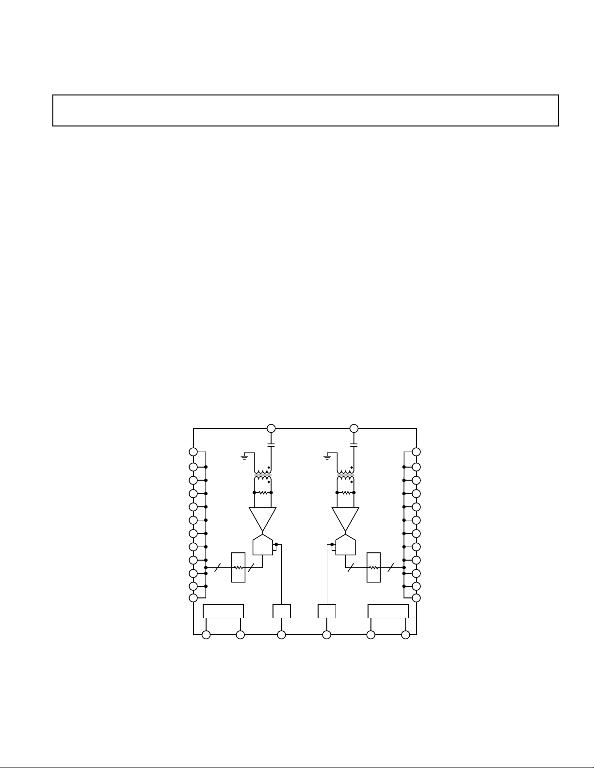
The AD10200 is a full channel ADC solution with on-module
signal conditioning for improved dynamic performance and
fully matched channel-to-channel performance. The module
Signal Conditioning
AD10200
includes two wide-dynamic range ADCs. Each ADC has a
transformer coupled front-end optimized for Direct-IF sampling.
The AD10200 has on-chip track-and-hold circuitry, and utilizes
an innovative architecture to achieve 12-bit, 105 MSPS performance. The AD10200 uses innovative high-density circuit
design to achieve exceptional matching and performance while
still maintaining excellent isolation, and providing for significant
board area savings.
The AD10200 operates with 5.0 V supply for the analog-todigital conversion. Each channel is completely independent
allowing operation with independent encode and analog inputs.
The AD10200 is packaged in a 68-lead ceramic chip carrier
package. Manufacturing is done on Analog Devices, Inc. MIL38534 Qualified Manufacturers Line (QML) and components
are available up to Class-H (–55°C to +125°C).
PRODUCT HIGHLIGHTS
1. Guaranteed sample rate of 105 MSPS.
2. Input signal conditioning with full power bandwidth to
250 MHz.
3. Fully tested/characterized performance at 121 MHz A
4. Optimized for IF sampling.
.
IN
FUNCTIONAL BLOCK DIAGRAM
AINA2
7
34
D00A
(LSB)
D01A
D02A
D03A
D04A
D05A
D06A
D07A
D08A
D09A
D10A
D11A
(MSB)
33
32
31
30
29
28
25
24
23
22
OUTPUT RESISTORS
21
18 17
12 12
TIMING
ENCODEAENCODEA
T1A
50⍀
T/H T/H
ADC
REF
3
REF_A_OUT
REV. A
Information furnished by Analog Devices is believed to be accurate and
reliable. However, no responsibility is assumed by Analog Devices for its
use, nor for any infringements of patents or other rights of third parties that
may result from its use. No license is granted by implication or otherwise
under any patent or patent rights of Analog Devices.
AINB2
63
50
D00B
(LSB)
49
T1B
50⍀
AD10200
ADC
12 12
OUTPUT RESISTORS
REF
56
REF_B_OUT
One Technology Way, P.O. Box 9106, Norwood, MA 02062-9106, U.S.A.
Tel: 781/329-4700 www.analog.com
Fax: 781/326-8703 © Analog Devices, Inc., 2001
TIMING
53 54
ENCODEBENCODEB
48
47
46
45
42
41
40
39
38
37
D01B
D02B
D03B
D04B
D05B
D06B
D07B
D08B
D09B
D10B
D11B
(MSB)

1
(V
AD10200–SPECIFICATIONS
= 3.3 V, VCC = 5.0 V; ENCODE = 105 MSPS, unless otherwise noted)
DD
Test MIL
Parameter Temp Level Subgroup Min Typ Max Unit
RESOLUTION 12 Bits
DC ACCURACY
Differential Nonlinearity Full IV 12 –0.99 ±0.5 +0.99 LSB
Integral Nonlinearity Full IV 12 –3 ± 0.75 +3 LSB
No Missing Codes Full I 1, 2, 3 Guaranteed
Gain Error
2
Full I 1, 2, 3 –9 ± 1+9% FS
Output Offset Full I 1, 2, 3 –12 +12 LSB
ANALOG INPUT
Input Voltage Range 25°C V 2.048 V p-p
Input Impedance 25°CV 50 Ω
Input VSWR
3
Full IV 12 1.1:1 1.25:1 Ratio
Analog Input Bandwidth, High Full IV 12 200 250 MHz
Analog Input Bandwidth, Low Full IV 12 1 MHz
ANALOG REFERENCE
Output Voltage Full I 1, 2, 3 2.4 2.5 2.6 V
Load Current 25°CV 5 mA
Tempco Full V 50 ppm/°C
SWITCHING PERFORMANCE
Maximum Conversion Rate Full I 4, 5, 6 105 MSPS
Minimum Conversion Rate Full IV 12 10 MSPS
Duty Cycle Full IV 12 45 50 55 %
Aperture Delay (t
Aperture Uncertainty (Jitter) 25°C V 0.25 ps rms
Output Valid Time (t
Output Propagation Delay (
Output Rise Time (t
)25°C V 1.0 ns
A
4
)
V
)25°C V 12 3.5 ns
R
PD
4
)
Full IV 12 3.0 5.3 ns
Full IV 12 4.5 5.5 8.0 ns
Output Fall Time (tF)25°C V 12 3.3 ns
DIGITAL INPUTS
Encode Input Common Mode Full IV 12 1.2 1.6 2.0 V
Differential Input (Enc, Enc) Full IV 12 0.4 5.0 V
Logic “1” Voltage Full IV 12 2.0 V
Logic “0” Voltage Full IV 12 0.8 V
Input Resistance Full IV 12 358kΩ
Input Capacitance 25°C V 4.5 pF
DIGITAL OUTPUTS
Logic “1” Voltage
Logic “0” Voltage
4
4
Full VI 1, 2, 3 3.1 3.3 V
Full VI 1, 2, 3 0 0.2 V
Output Coding Two’s Complement
POWER SUPPLY
Power Dissipation
5
6
Full I 1, 2, 3 1800 2200 mW
Power Supply Rejection Ratio Full IV 12 ± 0.5 ± 5 mV/V
I (DV
) Current Full I 1, 2, 3 25 40 mA
DD
I (AVCC) Current Full I 1, 2, 3 340 410 mA
DYNAMIC PERFORMANCE
Signal-to-Noise Ratio (SNR)
7
(Without Harmonics)
= 10 MHz 25°C V 67 dBFS
f
IN
Full V 66 dBFS
f
= 41 MHz 25°C I 4 64 66.5 dBFS
IN
Full II 5, 6 62 65 dBFS
= 71 MHz 25°C I 4 62.5 66.4 dBFS
f
IN
Full II 5, 6 61.5 64 dBFS
= 121 MHz 25°C I 4 61 65 dBFS
f
IN
Full II 5, 6 61 64 dBFS
–2–
REV. A

AD10200
Test MIL
Parameter Temp Level Subgroup Min Typ Max Unit
DYNAMIC PERFORMANCE
(Continued)
Signal-to-Noise Ratio (SINAD)
(With Harmonics)
f
= 10 MHz 25°C V 66 dBFS
IN
= 41 MHz 25°C I 4 63 65.5 dBFS
f
IN
f
= 71 MHz 25°C I 4 61 63.5 dBFS
IN
= 121 MHz 25°C I 4 56 58.5 dBFS
f
IN
Spurious Free Dynamic Range
fIN = 10 MHz 25°C V 81 dBFS
= 41 MHz 25°C I 4 73 81 dBFS
f
IN
f
= 71 MHz 25°C I 4 67 74 dBFS
IN
= 121 MHz 25°C I 4 61 65 dBFS
f
IN
Two-Tone Intermodulation
Distortion
f
f
f
10
(IMD)
= 10 MHz; fIN = 12 MHz 25°C V 86 dBc
IN
= 71 MHz; fIN = 72 MHz 25°C V 70 dBc
IN
= 121 MHz; fIN = 122 MHz 25°C I 4 55.5 62 dBc
IN
Channel-to-Channel Isolation
fIN = 121 MHz Full IV 12 80 85 dB
NOTES
1
All ac specifications tested by driving ENCODE and ENCODE differentially.
2
Gain Error measured at 2.5 MHz.
3
Input VSWR guaranteed 10 MHz to 200 MHz.
4
tV and tPD are measured from the transition points of the ENCODE input to the 50%/50% levels of the digital outputs swing. The digital output load during test is
not to exceed an ac load of 10 pF or a dc current of ± 40 mA.
5
Supply voltages should remain stable within ± 5% for normal operation.
6
Power dissipation measured with encode at rated speed and 0 dBm analog input.
7
Analog Input signal power at –1 dBFS; signal-to-noise ratio (SNR) is the ratio of signal level to total noise (first 5 harmonic removed). Encode = 105 MSPS. SNR
is reported in dBFS, related back to converter full scale.
8
Analog Input signal power at –1 dBFS; signal-to-noise and distortion (SINAD) is the ratio of signal level to total noise + harmonics. Encode = 105 MSPS. SINAD
is reported in dBFS, related back to converter full scale.
9
Analog Input signal equal –1 dBFS; SFDR is ratio of converter full scale to worst spur.
10
Both input tones at –7 dBFS; two tone intermodulation distortion (IMD) rejection is the ratio of either tone to the worst third order intermod product. f1 = x MHz
± 100 kHz, f2 = x MHz ± 100 kHz.
11
Channel-to-Channel isolation tested with A Channel/50 Ω terminated (AINA2) grounded and a full-scale signal applied to B Channel (AINB2).
Specifications subject to change without notice.
8
Full V 63 dBFS
Full II 5, 6 60.5 63 dBFS
Full II 5, 6 57 60 dBFS
9
Full II 5, 6 53 55 dBFS
Full V 70 dBFS
Full II 5, 6 67.5 dBFS
Full II 5, 6 60 dBFS
Full II 5, 6 55.5 58 dBFS
Full V 81 dBc
Full V 65 dBc
11
Full II 5, 6 53 57 dBc
REV. A
–3–

AD10200
ABSOLUTE MAXIMUM RATINGS
1, 2
VDD . . . . . . . . . . . . . . . . . . . . . . . . . . . . . . . . . . . . . . . . . 6 V
V
. . . . . . . . . . . . . . . . . . . . . . . . . . . . . . . . . . . . . . . . . 6 V
CC
Analog Inputs . . . . . . . . . . . . . . . . . . . . . . . . 5 V
Digital Inputs . . . . . . . . . . . . . . . . . . . –0.5 V to V
p-p(18 dBm)
+ 0.5 V
DD
Digital Output Current . . . . . . . . . . . . . . . . . . . . . . . . 20 mA
Operating Temperature . . . . . . . . . . . . . . . . –55°C to +125°C
Storage Temperature . . . . . . . . . . . . . . . . . . –65°C to +150°C
Maximum Junction Temperature . . . . . . . . . . . . . . . . . 175°C
Maximum Case Temperature . . . . . . . . . . . . . . . . . . . . 150°C
NOTES
1
Stresses above those listed under Absolute Maximum Ratings may cause perma-
nent damage to the device. This is a stress rating only; functional operation of the
device at these or any other conditions outside of those indicated in the operation
sections of this specification is not implied. Exposure to absolute maximum ratings
for extended periods may affect device reliability.
2
Typical thermal impedances for “Z” package:
θJC = 2.22°C/W; θJA = 24.3°C/W.
EXPLANATION OF TEST LEVELS
Test Level
I. 100% production tested.
II. 100% production tested at 25°C and sample tested at
specific temperatures.
III. Sample tested only.
IV. Parameter is guaranteed by design and characterization
testing.
V. Parameter is a typical value only.
VI. 100% production tested at 25°C; guaranteed by design and
characterization testing for industrial temperature range.
Table I. Output Coding (VREF = 2.5 V) (Two’s Complement)
Code AIN (V) Digital Output
+2047 +1.024 0111 1111 1111
•• •
•• •
0 0 0000 0000 0000
–1 –0.00049 1111 1111 1111
•• •
•• •
–2048 –1.024 1000 0000 0000
ORDERING GUIDE
Model Temperature Range Package Description Package Option
AD10200BZ –40°C to +85°C (Case) 68-Lead Ceramic Leaded Chip Carrier Z-68B
5962-9961002HXA –40°C to +85°C (Case) 68-Lead Ceramic Leaded Chip Carrier Z-68B
5962-9961001HXA –55°C to +125°C (Case) 68-Lead Ceramic Leaded Chip Carrier Z-68B
AD10200/PCB Evaluation Board with AD10200BZ
CAUTION
ESD (electrostatic discharge) sensitive device. Electrostatic charges as high as 4000 V readily
accumulate on the human body and test equipment and can discharge without detection. Although
WARNING!
the AD10200 features proprietary ESD protection circuitry, permanent damage may occur on
devices subjected to high-energy electrostatic discharges. Therefore, proper ESD precautions are
recommended to avoid performance degradation or loss of functionality.
ESD SENSITIVE DEVICE
–4–
REV. A

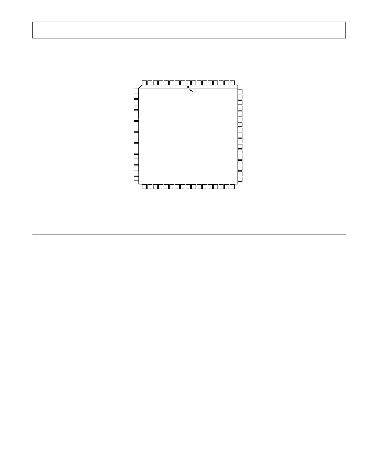
PIN CONFIGURATION
AD10200
CC
AV
D10B
DNC
AGNDB
D9B
D8B
B2
IN
A
D7B
NC
D6B
AGNDB
60
59
58
57
56
55
54
53
52
51
50
49
48
47
46
45
44
DGNDB
AGNDB
AGNDB
DNC
DNC
REF_B_OUT
AGNDB
ENCODEB
ENCODEB
AGNDB
DV
CC
D0B (LSB)
D1B
D2B
D3B
D4B
D5B
DGNDB
AGNDA
AGNDA
DNC
AGNDA
AV
DNC
AGNDA
ENCODEA
ENCODEA
AGNDA
DV
(MSB) D11A
D10A
D9A
D8A
D7A
DGNDA
A2
IN
NC
DNC
AGNDA
A
AGNDA
9618 7 6 5 68 67 66 65 64 63 624321
10
11
12
13
14
CC
15
16
17
18
19
20
CC
21
22
23
24
25
26
27 4328 29 30 31 32 33 34 35 36 37 38 39 40 41 42
D6A
D5A
D4A
DGNDA
NC = NO CONNECT
D3A
VREF_A_OUT
AGNDA
DNC
AD10200
TOP VIEW
(Not to Scale)
D2A
D1A
(LSB) D0A
SHIELD
PIN 1
IDENTIFIER
AGNDA
DNC
AGNDB
AGNDB
(MSB) D11B
PIN FUNCTION DESCRIPTIONS
Pin No. Mnemonic Function
1 SHIELD Internal Ground Shield between Channels
2, 5, 9–11, 13, 16, 19, 35 AGNDA A Channel Analog Ground. A and B grounds should be connected as close to
the device as possible.
3 VREF_A_OUT A Channel Internal Voltage Reference
6, 62 NC No Connection
7A
A2 Analog Input for A Side ADC
IN
4, 8, 12, 15, 57, 58, 64, 67 DNC Do Not Connect
14, 66 AV
CC
Analog Positive Supply Voltage (Nominally 5.0 V)
17 ENCODEA Complement of Encode
18 ENCODEA Data conversion initiated on the rising edge of ENCODE input.
20 DV
CC
Digital Positive Supply Voltage (Nominally 3.3 V)
21–25, 28–34 D11A–D7A, Digital Outputs for ADC A. D0 (LSB)
D6A–D0A
26, 27 DGNDA A Channel Digital Ground
36, 52, 55, 59–61, 65, 68 AGNDB B Channel Analog Ground. A and B grounds should be connected as close to
the device as possible.
37–42, 45–50 D11B–D6B, Digital Outputs for ADC B. D0 (LSB)
D5B–D0B
43, 44 DGNDB B Channel Digital Ground
51 DV
CC
Digital Positive Supply Voltage (Nominally 3.3 V)
53 ENCODEB Data conversion initiated on rising edge of ENCODE input.
54 ENCODEB Complement of Encode
56 VREF_B_OUT B Channel Internal Voltage Reference
63 AINB2 Analog Input for B Side ADC
REV. A
–5–

AD10200
DEFINITION OF SPECIFICATIONS
Analog Bandwidth
The analog input frequency at which the spectral power of the
fundamental frequency (as determined by the FFT analysis) is
reduced by 3 dB.
Aperture Delay
The delay between the 50% point on the rising edge of the
ENCODE command and the instant at which the analog input
is sampled.
Aperture Uncertainty (Jitter)
The sample-to-sample variation in aperture delay.
Differential Nonlinearity
The deviation of any code from an ideal 1 LSB step.
Encode Pulsewidth/Duty Cycle
Pulsewidth high is the minimum amount of time that the
ENCODE pulse should be left in Logic “1” state to achieve
rated performance; pulsewidth low is the minimum time
ENCODE pulse should be left in low state. At a given clock
rate, these specs define an acceptable Encode duty cycle.
Harmonic Distortion
The ratio of the rms signal amplitude to the rms value of the
worst harmonic component.
Integral Nonlinearity
The deviation of the transfer function from a reference line
measured in fractions of 1 LSB using a “best straight line”
determined by a least square curve fit.
Minimum Conversion Rate
The encode rate at which the SNR of the lowest analog signal
frequency drops by no more that 3 dB below the guaranteed limit.
Maximum Conversion Rate
The encode rate at which parametric testing is performed.
Output Propagation Delay
The delay between the 50% point of the rising edge of ENCODE
command and the time when all output data bits are within
valid logic levels.
Overvoltage Recovery Time
The amount of time required for the converter to recover to
0.02% accuracy after an analog input signal of the specified
percentage of full scale is reduced to midscale.
Power Supply Rejection Ratio
The ratio of a change in output offset voltage to a change in
power supply voltage.
Signal-to-Noise-and-Distortion (SINAD)
The ratio of the rms signal amplitude (set a 1 dB below full scale)
to the rms value of the sum of all other spectral components,
excluding the first five harmonics and dc. [May be reported in
dBc (i.e., degrades as signal levels is lowered) or in dBFS (always
related back to converter full scale)].
Signal-to-Noise Ratio (without Harmonics)
The ratio of the rms signal amplitude (set a I dB below full
scale) to the rms value of the sum of all other spectral components, excluding the first five harmonics and dc. [May be
reported in dBc (i.e., degrades as signal levels is lowered) or in
dBFS (always related back to converter full scale).]
Spurious-Free Dynamic Range
The ratio of the rms signal amplitude to the rms value of the
peak spurious spectral component. The peak spurious component may or may not be a harmonic. [May be reported in dBc
(i.e., degrades as signal levels is lowered) or in dBFS (always
related back to converter full scale).]
Transient Response
The time required for the converter to achieve 0.02% accuracy when a one-half full-scale step function is applied to the
analog input.
Two-Tone Intermodulation Distortion Rejection
The ratio of the rms value of either input tone to the rms value of
the worst third order intermodulation product; reported in dBc.
Voltage Standing-Wave Ratio (VSWR)
The ratio of the amplitude of the elective field at a voltage maximum to that at an adjacent voltage minimum.
–6–
REV. A
 Loading...