

Page 1
Quad Low Offset, Low Power
O
V
Data Sheet
FEATURES
Low input offset voltage: 150 µV (maximum)
Low offset voltage drift over –55°C to +125°C: 1.2 V/°C
(maximum)
Low supply current (per amplifier): 725 µA (maximum)
High open-loop gain: 5000 V/mV (minimum)
Input bias current: 3 nA (maximum)
Low noise voltage density: 11 nV/√Hz at 1 kHz
Stable with large capacitive loads: 10 nF typical
Available in die form
GENERAL DESCRIPTION
The OP400 is the first monolithic quad operational amplifier
that features OP77-type performance. Precision performance is
not sacrificed with the OP400 to obtain the space and cost savings
offered by quad amplifiers.
The OP400 features an extremely low input offset voltage of less
than 150 μV with a drift of less than 1.2 μV/°C, guaranteed over
the full military temperature range. Open-loop gain of the OP400
is more than 5 million into a 10 kΩ load, input bias current is
less than 3 nA, common-mode rejection (CMR) is more than
120 dB, and power supply rejection ratio (PSRR) is less than
1.8 μV/V. On-chip Zener zap trimming achieves the low input
offset voltage of the OP400 and eliminates the need for offset
Operational Amplifier
OP400
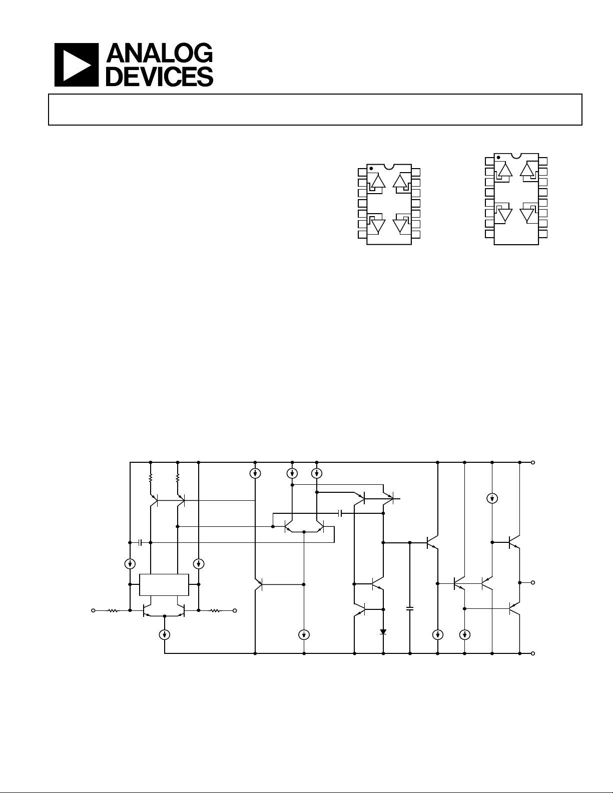
FUNCTIONAL BLOCK DIAGRAMS
OUTA
1
–IN A
OUT A
–IN A
+IN A
V+
+IN B
–IN B
UT B
1
2
3
4
5
6
7
–
+
OP400
–
+
14
OUT D
13
–IN D
–
+
+IN D
12
V–
11
+IN C
10
–
+
–IN C
9
OUT C
8
Figure 1. 14-Lead Ceramic Dual In-Line
Package [CERDIP] and 14-Lead Plastic
00304-001
2
–
+IN A
V+
+IN B
–IN B
OUT B
NC
+
3
4
OP400
5
–
+
6
7
8
NC = NO CONNECT
Figure 2. 16-Lead Standard Small
Outline Package [SOIC_W]
Dual In-Line Package [PDIP]
nulling. The OP400 conforms to the industry-standard quad
pinout, which does not have null terminals.
The OP400 features low power consumption, drawing less than
725 μA per amplifier. The total current drawn by this quad
amplifier is less than that of a single OP07, yet the OP400 offers
significant improvements over this industry-standard op amp.
Voltage noise density of the OP400 is a low 11 nV/√Hz at 10 Hz,
half that of most competitive devices.
The OP400 is an ideal choice for applications requiring multiple
precision operational amplifiers and where low power
consumption is critical.
OUT D
16
–IN D
15
–
+
+IN D
14
V–
13
+IN C
12
–
+
–IN C
11
OUT C
10
9
NC
+
00304-002
BIAS
VOLTAGE
LIMITING
NETWORK
+IN –IN
OUT
V–
0304-003
Figure 3. Simplified Schematic (One of Four Amplifiers Is Shown)
Rev. I Document Feedback
Information furnished by Analog Devices is believed to be accurate and reliable. However, no
responsibility is assumed by Analog Devices for its use, nor for any infringements of patents or other
rights of third parties that may result from its use. Specifications subject to change without notice. No
license is granted by implication or otherwise under any patent or patent rights of Analog Devices.
Trademarks and registered trademarks are the property of their respective owners.
One Technology Way, P.O. Box 9106, Norwood, MA 02062-9106, U.S.A.
Tel: 781.329.4700 ©2018 Analog Devices, Inc. All rights reserved.
Technical Support www.analog.com
Page 2

OP400 Data Sheet
TABLE OF CONTENTS
Features .............................................................................................. 1
Functional Block Diagrams ............................................................. 1
General Description ......................................................................... 1
Revision History ............................................................................... 2
Specifications ..................................................................................... 3
Electrical Characteristics ............................................................. 3
Absolute Maximum Ratings ............................................................ 5
Thermal Resistance ...................................................................... 5
ESD Caution .................................................................................. 5
REVISION HISTORY
5/2018—Rev. H to Rev. I
Changes to Figure 19 ........................................................................ 8
Changed Applications Section to Applications Information
Section .............................................................................................. 11
Changes to Ordering Guide .......................................................... 15
1/2013—Rev. G to Rev. H
Changes to Features Section and General Description Section ....... 1
Changes to Ordering Guide .......................................................... 15
2/2011—Rev. F to Rev. G
Added S Package to Storage Temperature Range in Table 4 ....... 5
Updated Outline Dimensions ....................................................... 15
12/2008—Rev. E to Rev. F
Added New Figure 28, Renumbered Sequentially ..................... 10
Updated Outline Dimensions ....................................................... 15
1/2007—Rev. D to Rev. E
Updated Format .................................................................. Universal
Changes to Figure 1 and Figure 2 ................................................... 1
Removed Figure 4 ............................................................................. 4
Changes to Table 3 ............................................................................ 4
Changes to Figure 16 through Figure 19, Figure 21..................... 8
Changes to Figure 27 ........................................................................ 9
Changes to Figure 28 ...................................................................... 10
Changes to Figure 33 ...................................................................... 13
Updated Outline Dimensions ....................................................... 14
3/2006—Rev. C to Rev. D
Updated Format .................................................................. Universal
Deleted Wafer Test Limits Table ..................................................... 4
New Package Drawing: R-14 ......................................................... 15
Updated Outline Dimensions ....................................................... 15
Changes to Ordering Guide .......................................................... 16
Typical Performance Characteristics ..............................................6
Applications Information .............................................................. 11
Dual Low Power Instrumentation Amplifier ......................... 11
Bipolar Current Transmitter ..................................................... 12
Differential Output Instrumentation Amplifier .................... 12
Multiple Output Tracking Voltage Reference ......................... 13
Outline Dimensions ....................................................................... 14
Ordering Guide .......................................................................... 15
SMD Parts and Equivalents ...................................................... 15
6/2003—Rev. B to Rev. C
Edits to Specifications ....................................................................... 2
10/2002—Rev. A to Rev. B
Addition of Absolute Maximum Ratings ....................................... 5
Edits to Outline Dimensions......................................................... 12
4/2002—Rev. 0 to Rev. A
Edits to Features................................................................................. 1
Edits to Ordering Information ........................................................ 1
Edits to Pin Connections .................................................................. 1
Edits to General Descriptions ..................................................... 1, 2
Edits to Package Type ....................................................................... 2
Rev. I | Page 2 of 15
Page 3

Data Sheet OP400
SPECIFICATIONS
ELECTRICAL CHARACTERISTICS
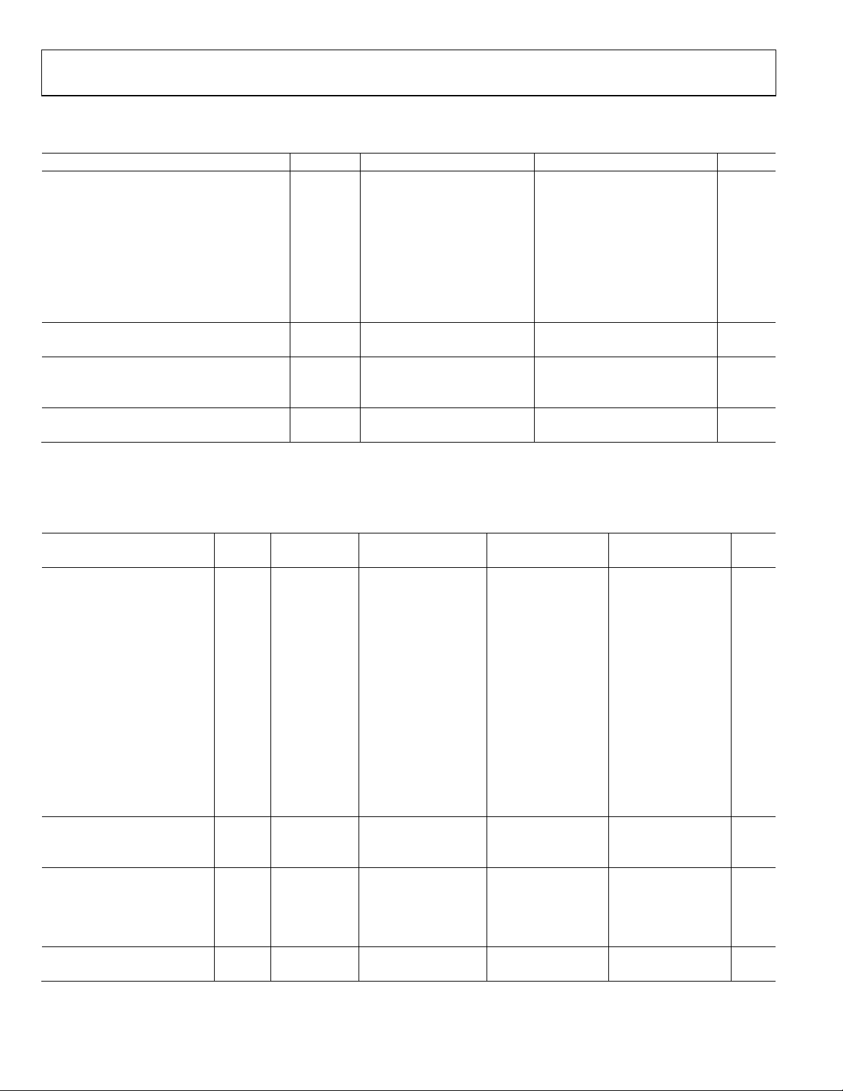
At VS = ±15 V, TA = +25°C, unless otherwise noted.
Table 1.
OP400A/E OP400F OP400G/H
Parameter Symbol Conditions Min Typ Max Min Typ Max Min Typ Max Unit
INPUT CHARACTERISTICS
Input Offset Voltage VOS 40 150 60 230 80 300 μV
Long-Term Input
Voltage Stability
Input Offset Current IOS VCM = 0 V 0.1 1.0 0.1 2.0 0.1 3.5 nA
Input Bias Current IB VCM = 0 V 0.75 3.0 0.75 6.0 0.75 7.0 nA
Input Noise Voltage e
Input Resistance
Differential Mode
Input Resistance
Common Mode
Large Signal Voltage
Gain
R
R
Input Voltage Range1 IVR ±12 ±13 ±12 ±13 ±12 ±13 V
Common-Mode
Rejection
Input Capacitance C
OUTPUT
CHARACTERISTICS
Output Voltage Swing VO RL = 10 kΩ ±12 ±12.6 ±12 ±12.6 ±12 ±12.6 V
POWER SUPPLY
Power Supply Rejection
Ratio
Supply Current per
Amplifier
DYNAMIC PERFORMANCE
Slew Rate SR 0.1 0.15 0.1 0.15 0.1 0.15 V/μs
Gain Bandwidth
Product
Channel Separation CS VO = 20 V p-p, 123 135 123 135 123 135 dB
f
Capacitive Load
Stability
NOISE PERFORMANCE
Input Noise Voltage en fO = 10 Hz3 22 36 22 36 22 nV/√Hz
Density3 f
Input Noise Current i
Input Noise Current
Density
1
Guaranteed by CMR test.
2
Guaranteed but not 100% tested.
3
Sample tested.
0.1 0.1 0.1 μV/mo
0.1 Hz to 10 Hz 0.5 0.5 0.5 μV p-p
n p-p
R
10 10 10 MΩ
IN
200 200 200 GΩ
R
INCM
VO = ±10 V
A
VO
= 10 kΩ 5000 12,000 3000 7000 3000 7000 V/mV
L
= 2 kΩ 2000 3500 1500 3000 1500 3000 V/mV
L
CMR V
3.2 3.2 3.2 pF
IN
= 12 V 120 140 115 140 110 135 dB
CM
PSRR V
No load 600 725 600 725 600 725 μA
I
SY
GBWP A
= 3 V to 18 V 0.1 1.8 0.1 3.2 0.2 5.6 μV/V
S
= 1 500 500 500 kHz
V
= 10 Hz2
O
AV = 1,
10 10 10 nF
no oscillations
= 1000 Hz3 11 18 11 18 11 nV/√Hz
O
0.1 Hz to 10 Hz 15 15 15 pA p-p
n p-p
i
fO = 10 Hz 0.6 0.6 0.6 pA/√Hz
n
Rev. I | Page 3 of 15
Page 4
OP400 Data Sheet
Input Offset Current
IOS
VCM = 0 V
0.1
2.5
nA
Common-Mode Rejection
CMR
VCM = ±12 V
115
130
dB
RL = 2 kΩ
±11
±12 ±11
±12 ±11
±12.2
V
At VS = ±15 V, −55°C ≤ TA ≤ +125°C for OP400A, unless otherwise noted.
Table 2.
Parameter Symbol Conditions Min Typ Max Unit
INPUT CHARACTERISTICS
Input Offset Voltage VOS 70 270 µV
Average Input Offset Voltage Drift TCVOS 0.3 1.2 µV/°C
Input Bias Current IB VCM = 0 V 1.3 5.0 nA
Large Signal Voltage Gain AVO VO = ±10 V, RL = 10 kΩ 3000 9000 V/mV
RL = 2 kΩ 1000 2300
Input Voltage Range1 IVR ±12 ±12.5 V
OUTPUT CHARACTERISTICS
Output Voltage Swing VO RL = 10 kΩ ±12 ±12.4
POWER SUPPLY
Power Supply Rejection Ratio PSRR VO = 3 V to 18 V 0.2 3.2 µV/V
Supply Current per Amplifier ISY No load 600 775 µA
DYNAMIC PERFORMANCE
Capacitive Load Stability AV = 1, no oscillations 8 nF
1
Guaranteed by CMR test.
At V
= ±15 V, −25°C ≤ TA ≤ +85°C for OP400E/F, 0°C ≤ TA ≤ 70°C for OP400G, −40°C ≤ TA ≤ +85°C for OP400H, unless otherwise noted.
S
Table 3.
OP400E OP400F OP400G/H
Parameter Symbol Conditions Min Typ Max Min Typ Max Min Typ Max Unit
INPUT CHARACTERISTICS
Input Offset Voltage VOS 60 220 80 350 110 400 µV
Average Input Offset
TCVOS 0.3 1.2 0.3 2.0 0.6 2.5 µV/°C
Voltage Drift
Input Offset Current IOS VCM = 0 V
E, F, G grades 0.1 2.5 0.1 3.5 0.2 6.0 nA
H grade 0.2 12.0 nA
Input Bias Current IB VCM = 0 V
E, F, G grades 0.9 5.0 0.9 10.0 1.0 12.0 nA
H grade 1.0 20.0 nA
Large-Signal Voltage Gain AVO VCM = 0 V
RL = 10 kΩ 3000 10,000 2000 5000 2000 5000 V/mV
RL = 2 kΩ 1500 2700 1000 2000 1000 2000 V/mV
Input Voltage Range1 IVR ±12 ±12.5 ±12 ±12.5 ±12 ±12.5 V
Common-Mode Rejection CMR VCM = ±12 V 115 135 110 135 105 130 dB
OUTPUT CHARACTERISTICS
Output Voltage Swing VO RL = 10 kΩ ±12 ±12.4 ±12 ±12.4 ±12 ±12.6 V
POWER SUPPLY
Power Supply Rejection
Ratio
Supply Current per
PSRR VS = ±3 V to
0.15 3.2 0.15 5.6 0.3 10.0 µV/V
±18 V
ISY No load 600 775 600 775 600 775 µA
Amplifier
DYNAMIC PERFORMANCE
Capacitive Load Stability No oscillations 10 10 10 nF
1
Guaranteed by CMR test.
Rev. I | Page 4 of 15
Page 5
Data Sheet OP400
ABSOLUTE MAXIMUM RATINGS
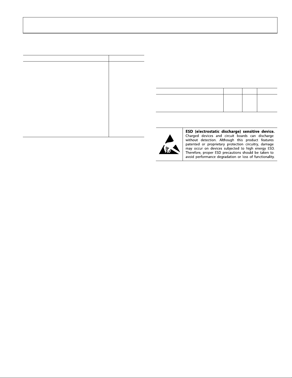
Table 4.
Parameter Rating
Supply Voltage ±20 V
Differential Input Voltage ±30 V
Input Voltage Supply voltage
Output Short-Circuit Duration Continuous
Storage Temperature Range
P, Y, S Packages −65°C to +150°C
Lead Temperature (Soldering 60 sec) 300°C
Junction Temperature (TJ) Range −65°C to +150°C
Operating Temperature Range
OP400A −55°C to +125°C
OP400E, OP400F −25°C to +85°C
OP400G 0°C to 70°C
OP400H −40°C to +85°C
Stresses at or above those listed under Absolute Maximum
Ratings may cause permanent damage to the product. This is a
stress rating only; functional operation of the product at these
or any other conditions above those indicated in the operational
section of this specification is not implied. Operation beyond
the maximum operating conditions for extended periods may
affect product reliability.
Absolute maximum ratings apply to both dice and packaged
parts, unless otherwise noted.
THERMAL RESISTANCE
θJA is specified for worst-case mounting conditions, that is, θJA is
specified for device in socket for CERDIP and PDIP packages;
θ
is specified for device soldered to printed circuit board for
JA
SOIC package.
Table 5. Thermal Resistance
Package Type θJA θJC Unit
14-Lead Ceramic DIP 94 10 °C/W
14-Lead Plastic DIP 76 33 °C/W
16-Lead SOIC 88 23 °C/W
ESD CAUTION
Rev. I | Page 5 of 15
Page 6
OP400 Data Sheet
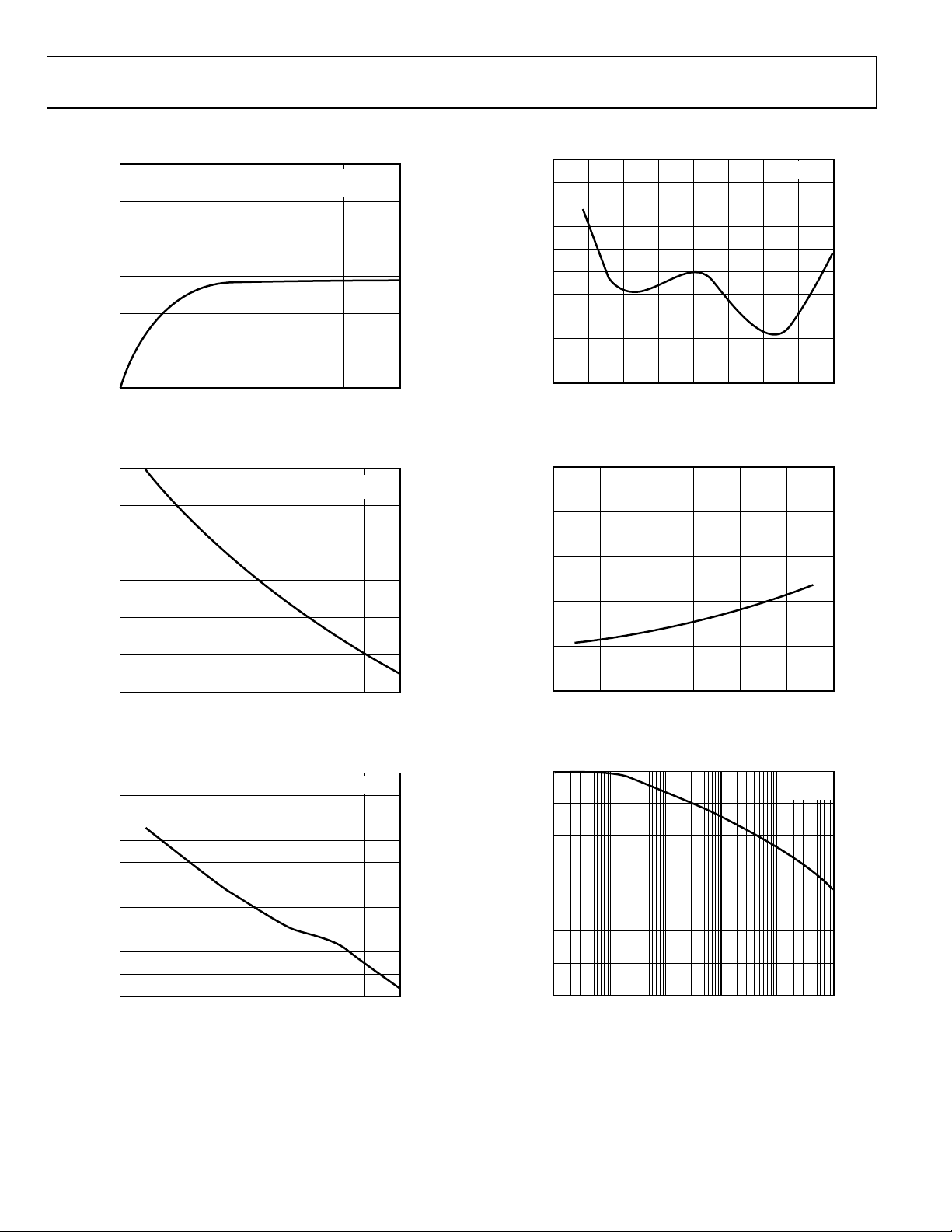
TYPICAL PERFORMANCE CHARACTERISTICS
3
TA = 25°C
= ±15V
V
S
120
VS = ±15V
2
1
CHANGE IN OFFSET VOLTAGE (μV)
0
0123 54
TIME (Minutes)
Figure 4. Warmup Drift
70
60
50
40
30
INPUT OFFSET VOLTAGE (μV)
20
VS = ±15V
110
100
90
INPUT OFFSET CURRENT ( pA)
80
00304-004
–75 1251007550250–25–50
TEMPERATURE (°C)
00304-007
Figure 7. Input Offset Current vs. Temperature
1.1
1.0
0.9
0.8
INPUT BIAS CURRENT (nA)
0.7
10
–75 1251007550250–25–50
TEMPERATURE (°C)
Figure 5. Input Offset Voltage vs. Temperature
2.0
1.6
1.2
0.8
INPUT BIAS CURRENT (nA)
0.4
0
–75 1251007550250–25–50
TEMPERATURE (°C)
Figure 6. Input Bias Current vs. Temperature
VS = ±15V
00304-005
0.6
–15 15105–5 0–10
COMMON-MODE VOLTAGE (V)
00304-008
Figure 8. Input Bias Current vs. Common-Mode Voltage
140
120
100
80
60
40
COMMON-MO DE REJECTIO N (dB)
20
00304-006
0
1 100k10k100 1k10
FREQUENCY (Hz)
TA =25°C
= ±15V
V
S
00304-009
Figure 9. Common-Mode Rejection vs. Frequency
Rev. I | Page 6 of 15
Page 7
Data Sheet OP400
100
10
1
1k
100
10
00304-010
NOISE VOLTAGE DENSITY (nV/ Hz)
FREQUENCY (Hz )
1k
0
200
400
600
800
1
1k
10010
00304-011
CURRENT NOISE DE NS ITY (fA/ Hz )
FREQUENCY (Hz )
T
A
=
25
°C
V
S
= ±15V
0 104 6 82
00304-012
TIME (Seconds)
2.5
2.1
2.2
2.3
2.4
±2 ±6 ±10 ±14 ±18±4 ±8 ±12 ±16 ±20
00304-013
TOTAL S UP P LY CURRENT (mA)
SUPPLY VOLTAGE (V)
FOUR AMPLIFIERS
TA = 25°C
2.5
2.1
2.2
2.3
2.4
–75 –50 –25 0 25 50 75 100 125 150
00304-014
TOTAL S UPP LY CURRENT (mA)
TEMPERATURE (°C)
FOUR AMPLIFIERS
V
S
= ±15V
140
0
20
40
60
80
100
120
0.1 100k10k1k100101
00304-015
POWER SUPPLY REJECTION (dB)
FREQUENCY (Hz )
NEGATIVE
SUPPLY
POSITIVE
SUPPLY
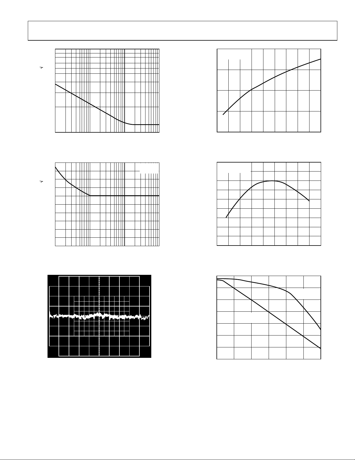
Figure 10. Noise Voltage Density vs. Frequency
Figure 11. Current Noise Density vs. Frequency
Figure 13. Total Supply Current vs. Supply Voltage
Figure 14. Total Supply Current vs. Temperature
Figure 12. 0.1 Hz to 10 Hz Noise
Figure 15. Power Supply Rejection vs. Frequency
Rev. I | Page 7 of 15
Page 8
OP400 Data Sheet
144
VS= ±15V
142
140
138
136
POWER SUPPLY REJECTI ON (dB)
80
AV = 1000
60
AV = 100
40
GAIN (dB)
AV = 10
20
AV= 1
0
TA = 25°C
= ±15V
V
S
134
–75 1501251007550250–25–50
TEMPERATURE (° C)
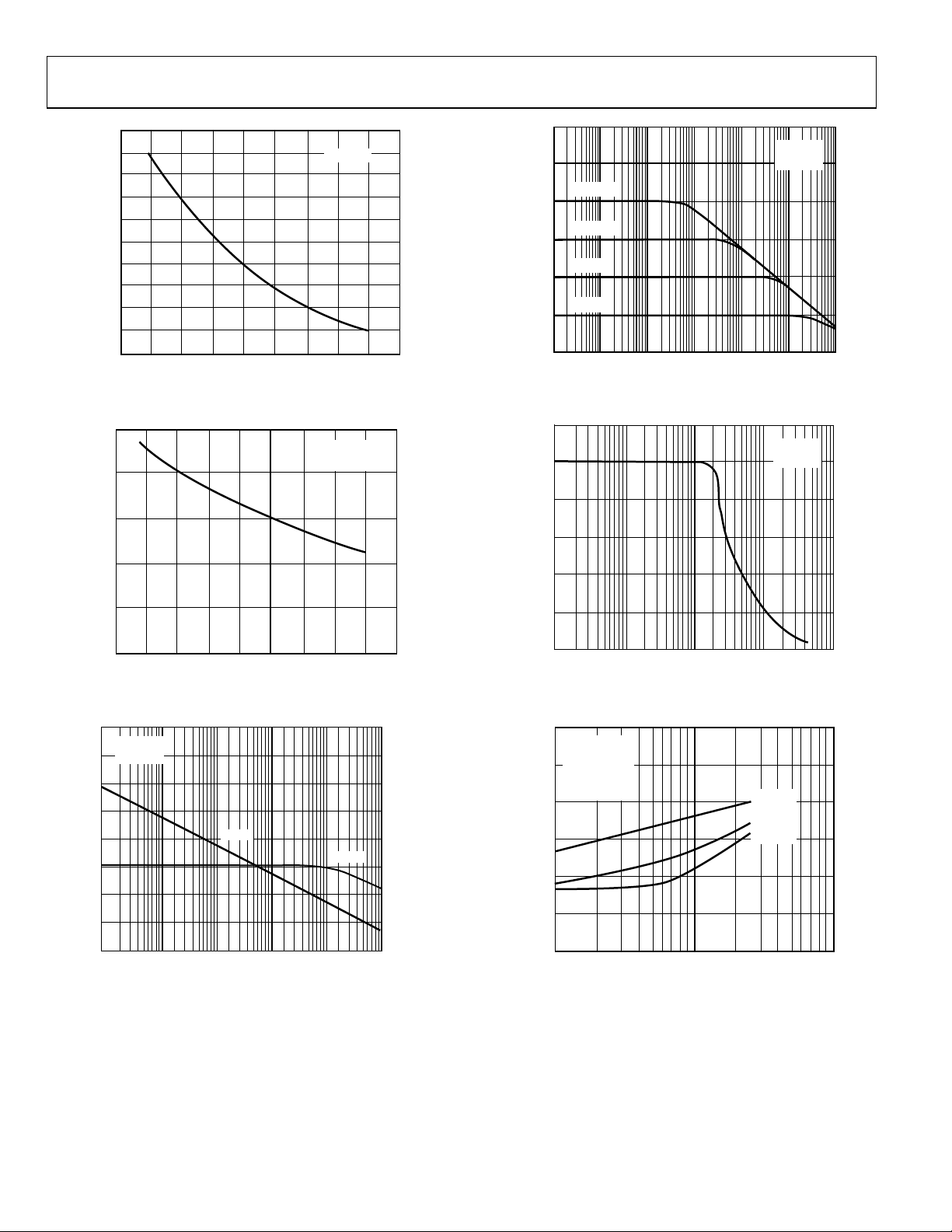
Figure 16. Power Supply Rejection vs. Temperature
5k
4k
3k
2k
OPEN-LOOP GAIN (V/mV)
1k
0
–75 1501251007550250–25–50
TEMPERATURE (°C)
Figure 17. Open-Loop Gain vs. Temperature
TA = 25°C
120
V
= ±15V
S
100
80
60
40
OPEN-LOOP GAIN (dB)
20
0
10 1M10k 100k1k100
GAIN
FREQUENCY (Hz)
Figure 18. Open-Loop Gain and Phase Shift vs. Frequency
VS = ±15V
R
=2kΩ
L
PHASE
0
45
90
135
180
00304-016
110 1k100 100k10k 1M
FREQUENCY (Hz)
00304-019
Figure 19. Closed-Loop Gain vs. Frequency
TA = 25°C
V
= ±15V
25
20
15
10
5
OUTPUT SWING (V p-p AT 1% Distortion)
00304-017
10 100 1k 10k 100k
FREQUENCY (Hz)
S
00304-020
Figure 20. Maximum Output Swing Frequency
TA = 25°C
V
= ±15V
S
10
V
= 10V p-p
OUT
R
= 2kΩ
L
1
0.1
DISTORTION (%)
PHASE SHIFT (Degrees)
00304-018
0.01
0.001
100 1k 10k
FREQUENCY (Hz)
AV = 100
= 10
A
V
A
= 1
V
000304-021
Figure 21. Total Harmonic Distortion vs. Frequency
Rev. I | Page 8 of 15
Page 9
Data Sheet OP400
50
TA = 25°C
45
V
= ±15V
S
40
A
= +1
V
35
30
25
20
OVERSHOOT (%)
15
10
5
0
0 0.5 1.0 2.0 2.51.5 3.0
CAPACITIVE LOAD (nF)
FALLING
RISING
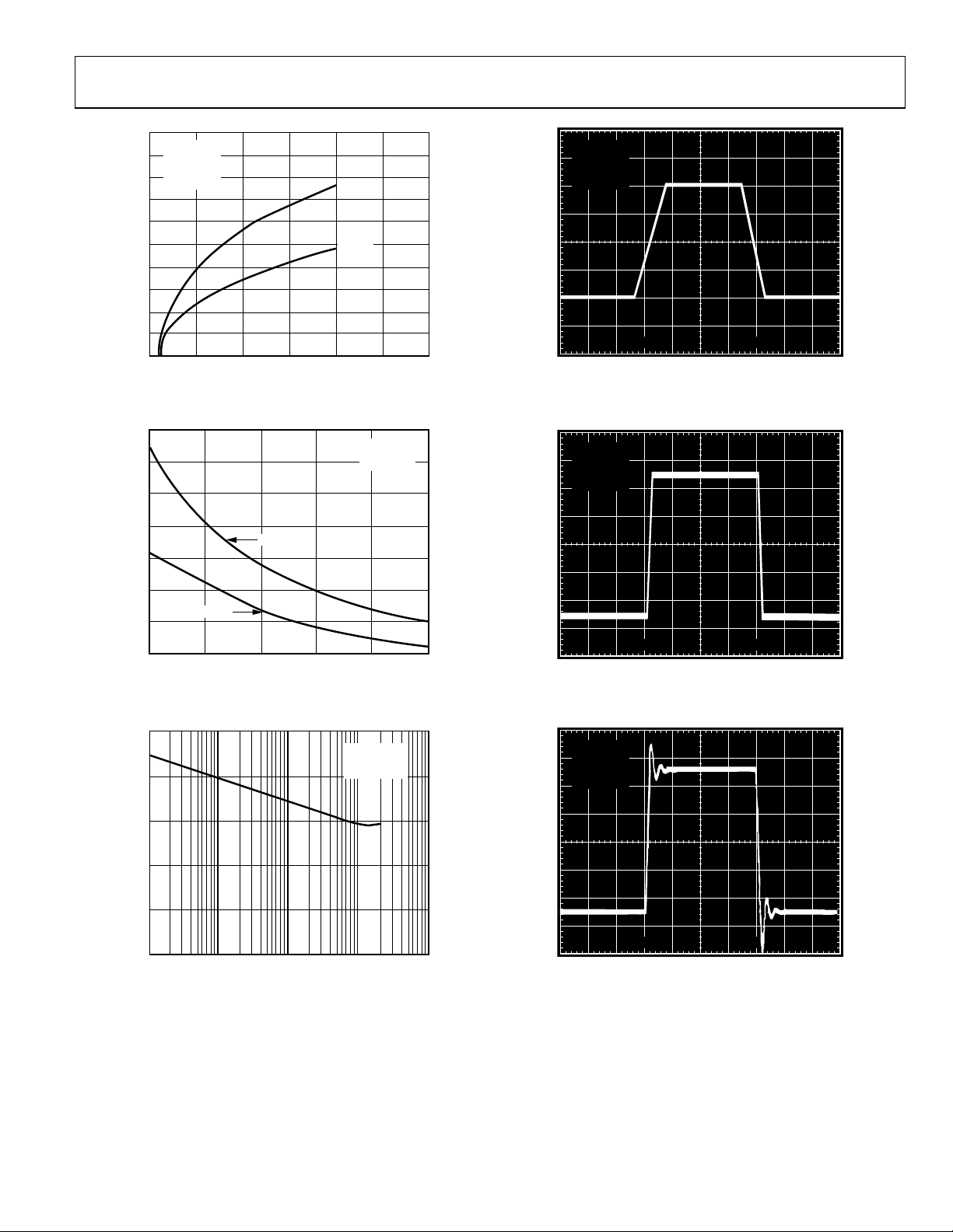
Figure 22. Overshoot vs. Capacitive Load
000304-022
TA = 25°C
= ±15V
V
S
A
= +1
V
5V 100μs
Figure 25. Large Signal Transient Response
00304-025
34
32
30
SHORT-CIRCUI T CURRENT (mA)
SOURCING
28
01 234 5
SINKING
TIME (Minutes)
TA = 25°C
= ±15V
V
S
Figure 23. Short Circuit vs. Time
140
TA = 25°C
= ±15V
V
S
= 20V p-p
V
130
120
110
IN
TA = 25°C
V
= ±15V
S
A
= +1
V
00304-023
20mV 5μs
00304-026
Figure 26. Small Signal Transient Response
TA = 25°C
V
= ±15V
S
A
= +1
V
CHANNEL SEPARATIO N (dB)
100
90
10 100 1k 10k 100k
FREQUENCY (Hz)
Figure 24. Channel Separation vs. Frequency
00304-024
Rev. I | Page 9 of 15
20mV 5μs
Figure 27. Small Signal Transient Response, C
LOAD
= 1 nF
00304-027
Page 10
OP400 Data Sheet
–18V
10k
VDD – V
OH
–
1/4
OP400
+
1k
SATURATIO N VOLTAG E (mV)
OP400
= ±15V
V
SY
= 25°C
T
A
100
0.001 0.01 0.1 1 10
OUTPUT CURRENT (mA)
VOL – V
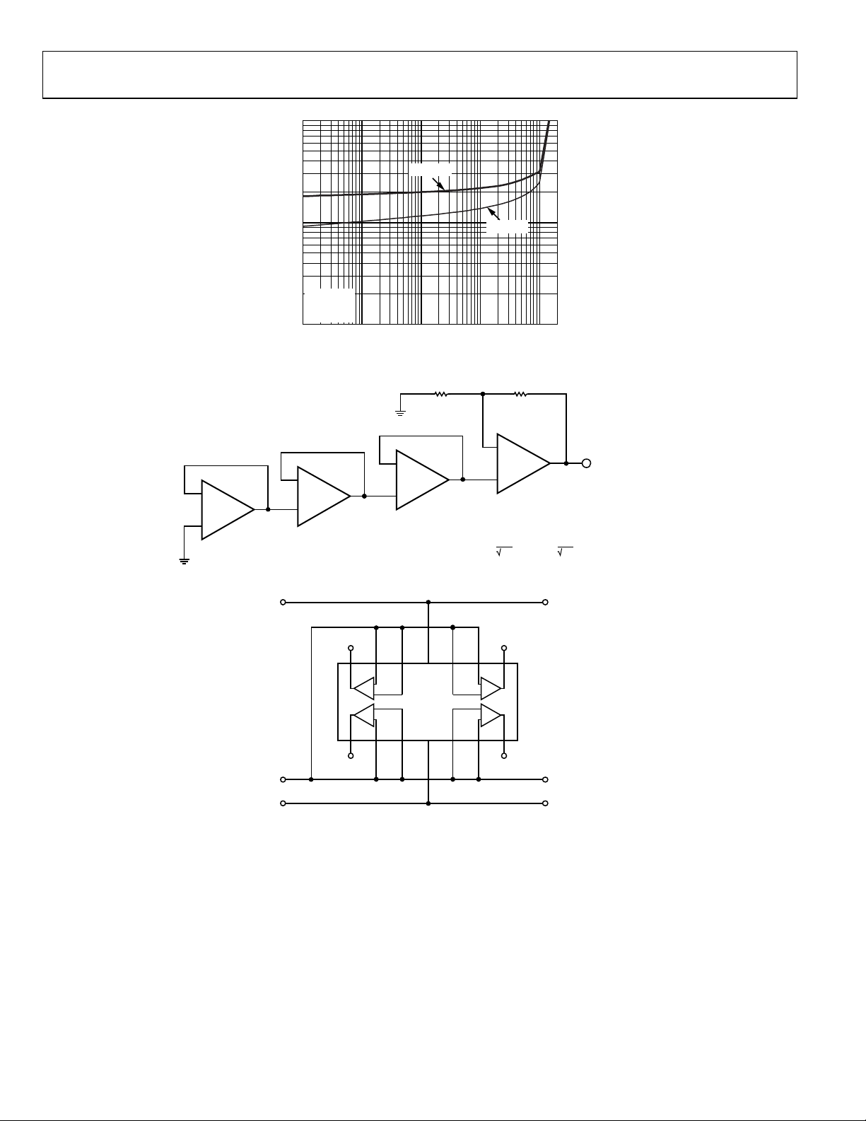
Figure 28. Saturation Voltage vs. Output Current
100Ω 10kΩ
–
–
1/4
OP400
1/4
OP400
+
+
e
( )
OUT
Figure 29. Noise Test Schematic
SS
20
–
1/4
OP400
+
TO SPECTRUM ANALYZER
nV
Hz
nV
~
( )
2 × e
=
n
Hz
00304-035
× 101
e
OUT
00304-028
14 13 12 11 10 9 8
GND
+18V
–
4
+
+
1
–
1234567
V–
V+
–
3
+
+
2
–
00304-029
Figure 30. Burn-In Circuit
Rev. I | Page 10 of 15
Page 11
Data Sheet OP400
10
67 kHz
–
+
20kΩ5kΩ5kΩ
20kΩ
REFERENCE
V
IN
V
IN
R
G
R
G
V
OUT
V
OUT
–
+
20kΩ5kΩ5kΩ
20kΩ
REFERENCE
V
IN
R
G
V
OUT
40,000
= 5 +
00304-030
1/4
OP400A
+
–
1/4
OP400A
+
–
1/4
OP400A
+
–
1/4
OP400A
+
–
APPLICATIONS INFORMATION
The OP400 is inherently stable at all gains and is capable of
driving large capacitive loads without oscillating. Nonetheless,
good supply decoupling is highly recommended. Proper supply
decoupling reduces problems caused by supply line noise and
improves the capacitive load-driving capability of the OP400.
Total supply current can be reduced by connecting the inputs of
an unused amplifier to V−. This turns the amplifier off, lowering
the total supply current.
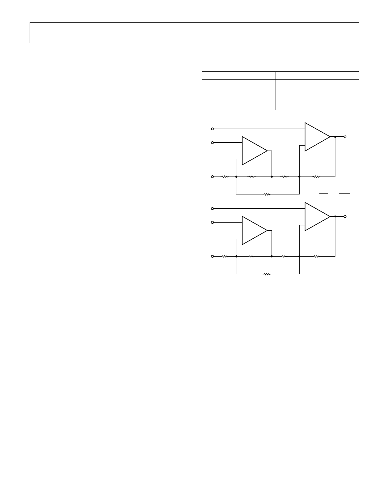
DUAL LOW POWER INSTRUMENTATION AMPLIFIER
A dual instrumentation amplifier that consumes less than 33 mW
of power per channel is shown in Figure 31. The linearity of the
instrumentation amplifier exceeds 16 bits in gains of 5 to 200 and
is better than 14 bits in gains from 200 to 1000. Common-mode
rejection ratio (CMRR) is above 115 dB (G = 1000). Offset voltage
drift is typically 0.4 μV/°C over the military temperature range,
which is comparable to the best monolithic instrumentation
amplifiers. The bandwidth of the low power instrumentation
amplifier is a function of gain and is shown in Table 6.
The output signal is specified with respect to the reference input,
which is normally connected to analog ground. The reference
input can offset the output from −10 V to +10 V if required.
Table 6. Gain Bandwidth
Gain Bandwidth
5 150 kHz
100 7.5 kHz
1000 500 Hz
Figure 31. Dual Low Power Instrumentation Amplifier
Rev. I | Page 11 of 15
Page 12
OP400 Data Sheet
00304-031
–
+
V
OUT
I
OUT
5mA
I
OUT
V
IN
50,000
200Ω
200Ω
R
G
25kΩ
25kΩ
25kΩ
25kΩ
25kΩ 25kΩ
R
G
– –
1
V
IN
1/4
OP400E
+
–
1/4
OP400E
+
–
1/4
OP400E
+
–
1/4
OP400E
+
–
–
+
00304-032
V
OUT
VINR
G
25kΩ
25kΩ
25kΩ
25kΩ
25kΩ
22pF
22pF
22pF
22pF
25kΩ
25kΩ
25kΩ
V
OUT
V
IN
=
50kΩ + R
G
R
G
REFERENCE
INPUT
1/4
OP400A
+
–
1/4
OP400A
+
–
1/4
OP400A
+
–
1/4
OP400A
+
–
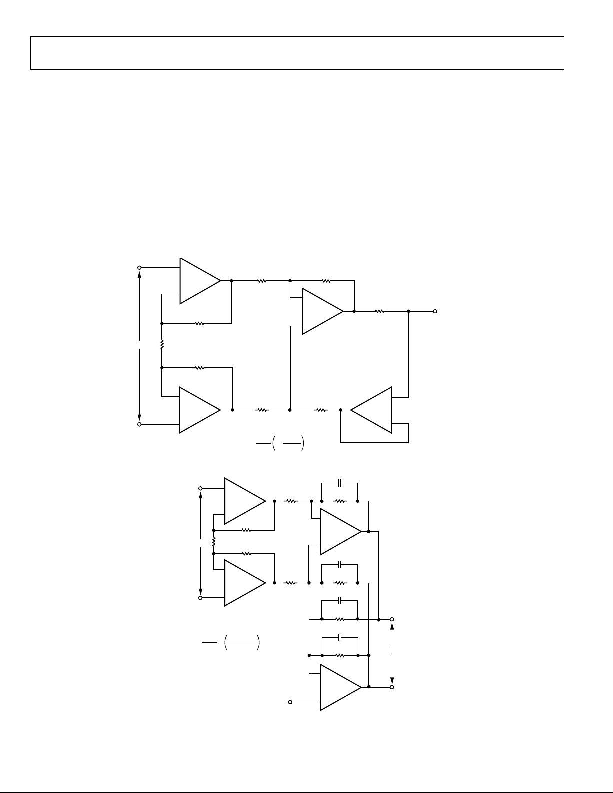
BIPOLAR CURRENT TRANSMITTER
In the circuit of Figure 32, which is an extension of the standard
three op amp instrumentation amplifier, the output current is
proportional to the differential input voltage. Maximum output
current is ±5 mA, with voltage compliance equal to ±10 V when
using ±15 V supplies. Output impedance of the current transmitter
exceeds 3 MΩ, and linearity is better than 16 bits with gain set
for a full-scale input of ±100 µV.
DIFFERENTIAL OUTPUT INSTRUMENTATION AMPLIFIER
The output voltage swing of a single-ended instrumentation
amplifier is limited by the supplies, normally at ±15 V, to a
maximum of 24 V p-p. The differential output instrumentation
amplifier shown in Figure 33 can provide an output voltage
swing of 48 V p-p when operated with ±15 V supplies. The
extended output swing is due to the opposite polarity of the
outputs. Both outputs swing 24 V p-p, but with opposite polarity,
for a total output voltage swing of 48 V p-p. The reference input can
set a common-mode output voltage over the range ±10 V. The
PSRR of the amplifier is less than 1 µV/V with CMRR (G = 1000)
better than 115 dB. Offset voltage drift is typically 0.4 µV/°C over
the military temperature range.
Figure 32. Bipolar Current Transmitter
Figure 33. Differential Output Instrumentation Amplifier
Rev. I | Page 12 of 15
Page 13
Data Sheet OP400
7.5V
10V
5V
2.5V
10kΩ
10kΩ
10kΩ
10kΩ
15V
22kΩ
10kΩ
1N4002
10kΩ
10kΩ
2μF
1μF
1μF
4
2
6
00304-033
REF 43
2.5V
REFERENCE
1/4
OP400A
+
–
1/4
OP400A
+
–
1/4
OP400A
+
–
1/4
OP400A
+
–
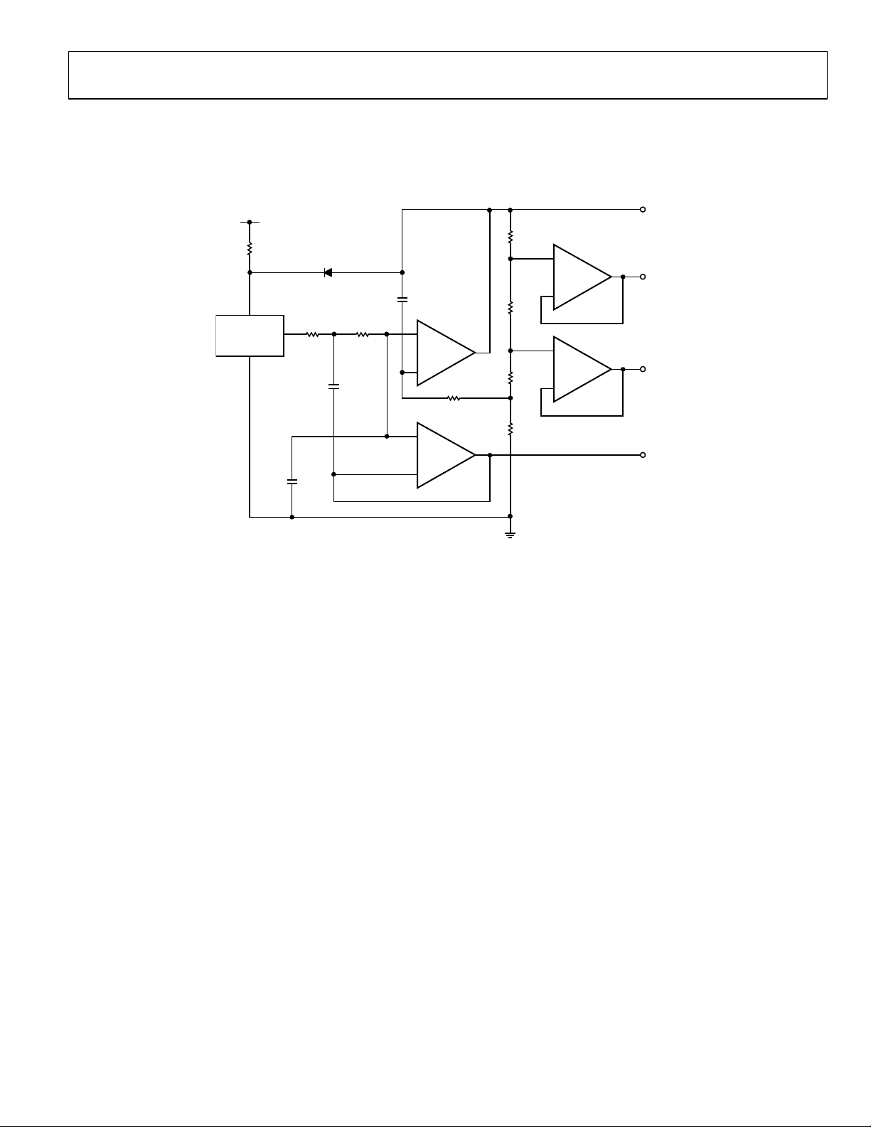
MULTIPLE OUTPUT TRACKING VOLTAGE REFERENCE
Figure 34 shows a circuit that provides outputs of 10 V, 7.5 V,
5 V, and 2.5 V for use as a system voltage reference. Maximum
output current from each reference is 5 mA with load regulation
under 25 µV/mA. Line regulation is better than 15 µV/V, an d
output voltage drift is under 20 µV/°C. Output voltage noise
from 0.1 Hz to 10 Hz is typically 75 µV p-p from the 10 V output
and proportionately less from the 7.5 V, 5 V, and 2.5 V outputs.
Figure 34. Multiple Output Tracking Voltage Reference
Rev. I | Page 13 of 15
Page 14
OP400 Data Sheet
OUTLINE DIMENSIONS
0.210 (5.33)
0.150 (3.81)
0.130 (3.30)
0.110 (2.79)
0.022 (0.56)
0.018 (0.46)
0.014 (0.36)
0.005 (0.13) MIN
PIN 1
0.785 (19.94) MAX
0.200 (5.08)
MAX
0.200 (5.08)
0.125 (3.18)
0.023 (0.58)
0.014 (0.36)
CONTROLLING DIMENSIONS ARE IN INCHES; MILLIMETER DIMENSIONS
(IN PARENTHESES) ARE ROUNDED-OFF INCH EQUIVALENTS FOR
REFERENCE ONLY AND ARE NOT APPROPRIATE FOR USE IN DESIGN.
0.098 (2.49) MAX
1
0.100 (2.54) BSC
0.070 (1.78)
0.030 (0.76)
814
7
0.310 (7.87)
0.220 (5.59)
0.060 (1.52)
0.015 (0.38)
0.150
(3.81)
MIN
SEATING
PLANE
0.320 (8.13)
0.290 (7.37)
15°
0°
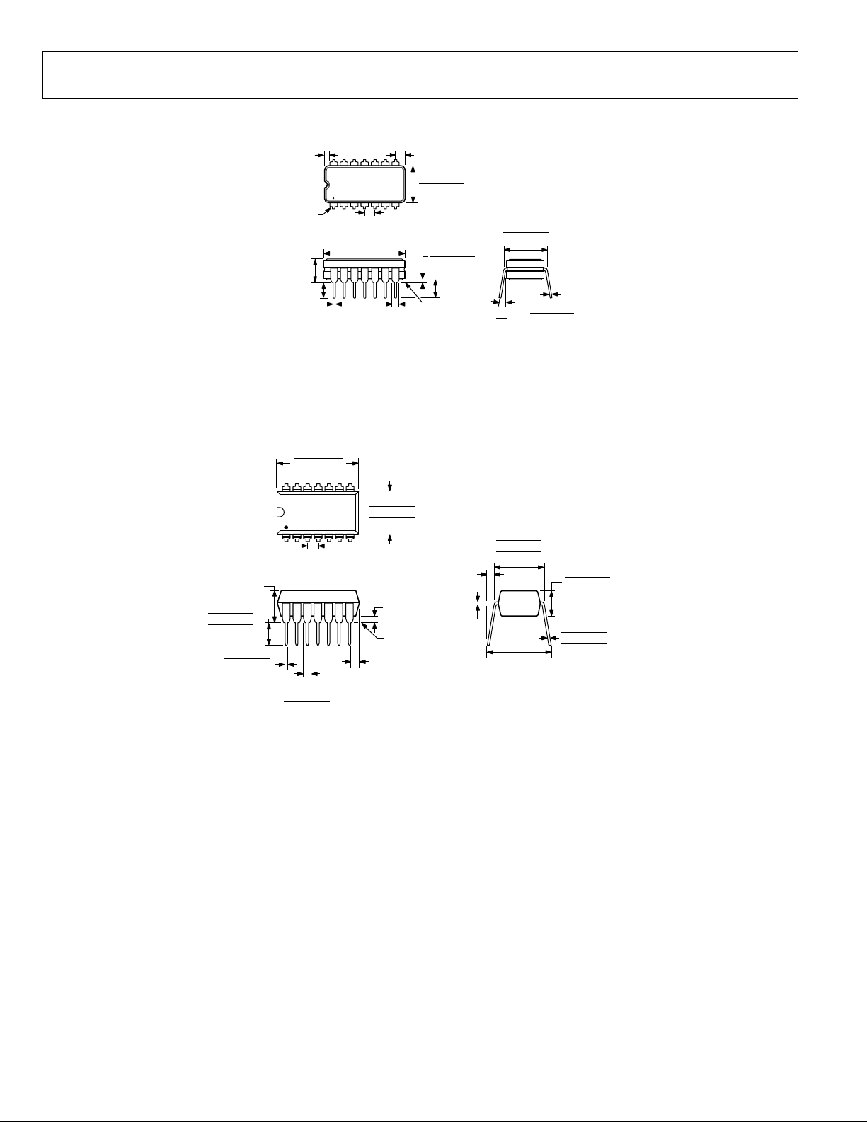
Figure 35. 14-Lead Ceramic Dual In-Line Package [CERDIP]
(Q-14)
Dimensions shown in inches and (millimeters)
0.775 (19.69)
0.750 (19.05)
0.735 (18.67)
MAX
14
1
0.100 (2.54)
BSC
0.070 (1.78)
0.050 (1.27)
0.045 (1.14)
8
7
0.280 (7. 11)
0.250 (6.35)
0.240 (6.10)
0.015
(0.38)
MIN
SEATING
PLANE
0.005 (0.13)
MIN
0.060 (1.52)
MAX
0.015 (0.38)
GAUGE
PLANE
0.325 (8.26)
0.310 (7.87)
0.300 (7.62)
0.430 (10.92)
0.015 (0.38)
0.008 (0.20)
0.195 (4.95 )
0.130 (3.30 )
0.115 (2.92)
0.014 (0.36)
0.010 (0.25)
0.008 (0.20)
MAX
CONTROL LING DIMENSIONS ARE IN INCHE S ; M ILLIME TER DIMENSIONS
(IN PARENTHESES) ARE ROUNDED-OFF INCH EQUIVALENTS FOR
REFERENCE O NLYAND ARE NOT APPROP RIATE FOR USE I N DE S IGN.
CORNER LEADS MAY BE CONFIGURED AS WHOLE O R HALF LEADS .
COMPLIANT TO JEDEC STANDARDS MS-001
Figure 36. 14-Lead Plastic Dual In-Line Package [PDIP]
Narrow Body
(N-14)
Dimensions shown in inches and (millimeters)
Rev. I | Page 14 of 15
070606-A
Page 15
Data Sheet OP400
C
0.30 (0.0118)
0.10 (0.0039)
OPLANARITY
0.10
10.50 (0.4134)
10.10 (0.3976)
BSC
9
7.60 (0.2992)
7.40 (0.2913)
8
10.65 (0.4193)
10.00 (0.3937)
2.65 (0.1043)
2.35 (0.0925)
SEATING
PLANE
8°
0°
0.33 (0.0130)
0.20 (0.0079)
5
0
.7
0
.
2
5
16
1
1.27 (0.0500)
0.51 (0.0201)
0.31 (0.0122)
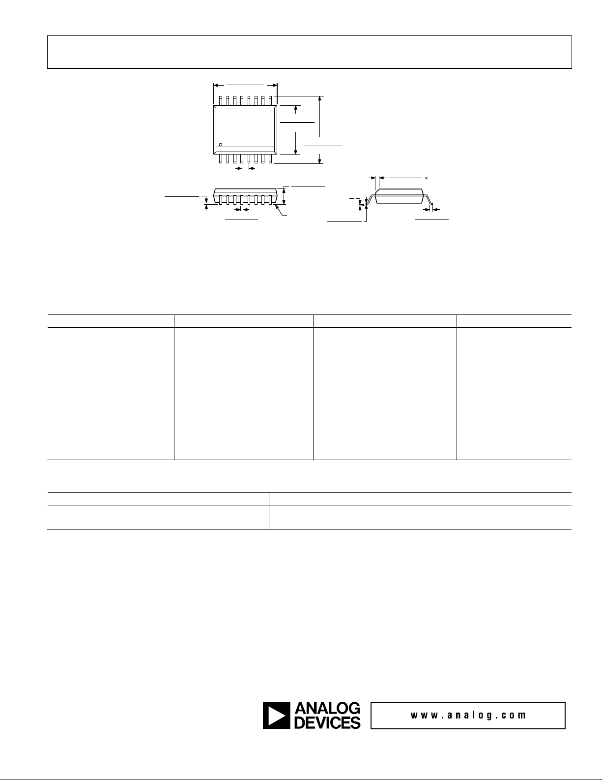
CONTROLLING DIMENSIONS ARE IN MILLIMETERS; INCH DIMENSIONS
(IN PARENTHESES) ARE ROUNDED-OFF MILLIMETER EQUIVALENTS FOR
REFERENCE ONLYAND ARE NOT APPROPRIATEFOR USE IN DESIGN.
COMPLIANT TO JEDEC STANDARDS MS-013-AA
Figure 37. 16-Lead Standard Small Outline Package [SOIC_W]
0
2
9
(
0
.
(
0
.
0
0
9
1.27 (0.0500)
0.40 (0.0157)
5
)
45°
8
)
03-27-2007-B
Wide Body (RW-16)
Dimensions shown in millimeters and (inches)
ORDERING GUIDE
Model1 Temperature Range Package Description Package Option
OP400AY −55°C to +125°C 14-Lead CERDIP Q-14
OP400EY −25°C to +85°C 14-Lead CERDIP Q-14
OP400FY −25°C to +85°C 14-Lead CERDIP Q-14
OP400GPZ 0°C to +70°C 14-Lead PDIP N-14
OP400HPZ −40°C to +85°C 14-Lead PDIP N-14
OP400GS 0°C to +70°C 16-Lead SOIC_W RW-16
OP400GSZ 0°C to +70°C 16-Lead SOIC_W RW-16
OP400GSZ-REEL 0°C to +70°C 16-Lead SOIC_W RW-16
OP400HSZ −40°C to +85°C 16-Lead SOIC_W RW-16
OP400HSZ-REEL −40°C to +85°C 16-Lead SOIC_W RW-16
OP400GBC Die
1
Z = RoHS Compliant Part.
SMD PARTS AND EQUIVALENTS
SMD Part Number1 Analog Devices Equivalent
5962-8777101M3A OP400ATCMDA
5962-8777101MCA OP400AYMDA
1
For military processed devices, please refer to the standard microcircuit drawing (SMD) available at the Defense Supply Center Columbus website.
©2018 Analog Devices, Inc. All rights reserved. Trademarks and
registered trademarks are the property of their respective owners.
D00304-0-5/18(I)
Rev. I | Page 15 of 15
 Loading...