

Page 1

Data Sheet
ADuM1200/ADuM1201
Dual-Channel Digital Isolators
FEATURES
► Narrow body, RoHS-compliant, SOIC 8-lead package
► Low power operation
► 5 V operation
1.1 mA per channel maximum at 0 Mbps to 2 Mbps
►
► 3.7 mA per channel maximum at 10 Mbps
► 8.2 mA per channel maximum at 25 Mbps
► 3 V operation
► 0.8 mA per channel maximum at 0 Mbps to 2 Mbps
► 2.2 mA per channel maximum at 10 Mbps
► 4.8 mA per channel maximum at 25 Mbps
► Bidirectional communication
► 3 V/5 V level translation
► High temperature operation: 125°C
► High data rate: dc to 25 Mbps (NRZ)
► Precise timing characteristics
► 3 ns maximum pulse width distortion
► 3 ns maximum channel-to-channel matching
► High common-mode transient immunity: >25 kV/µs
► Safety and regulatory approvals
► UL 1577
► V
= 2500 V
ISO
► IEC/EN/CSA 62368-1
► IEC/CSA 61010-1
► CQC GB4943.1
► DIN EN IEC 60747-17 (VDE 0884-17)
► V
► AEC-Q100 qualified for automotive applications
= 560 V
IORM
for 1 minute
RMS
PEAK
APPLICATIONS
GENERAL DESCRIPTION
The ADuM1200/ADuM1201
1
are dual-channel digital isolators
based on the Analog Devices, Inc., iCoupler® technology. Combining high speed CMOS and monolithic transformer technologies,
these isolation components provide outstanding performance characteristics superior to alternatives, such as optocouplers.
By avoiding the use of LEDs and photodiodes, iCoupler devices
remove the design difficulties commonly associated with opto-couplers.
The typical optocoupler concerns regarding uncertain current transfer ratios, nonlinear transfer functions, and temperature and lifetime
effects are eliminated with the simple iCoupler digital interfaces and
stable performance characteristics. The need for external drivers
and other discrete components is eliminated with these iCoupler
products. Furthermore, iCoupler devices consume one-tenth to
one-sixth the power of optocouplers at comparable signal data
rates.
The ADuM1200/ADuM1201 isolators provide two independent isolation channels in a variety of channel configurations and data rates
(see the Ordering Guide). Both devices operate with the supply
voltage on either side ranging from 2.7 V to 5.5 V, providing compatibility with lower voltage systems as well as enabling a voltage
translation functionality across the isolation barrier. In addition, the
ADuM1200/ADuM1201 provide low pulse width distortion (<3 ns for
CR grade) and tight channel-to-channel matching (<3 ns for CR
grade). Unlike other optocoupler alternatives, the ADuM1200/ADuM1201 isolators have a patented refresh feature that ensures dc
correctness in the absence of input logic transitions and during
power-up/power-down conditions.
The ADuM1200W and ADuM1201W are automotive grade versions
qualified for 125°C operation. See the Automotive Products section
for more information.
► Size-critical multichannel isolation
► SPI interface/data converter isolation
► RS-232/RS-422/RS-485 transceiver isolation
► Digital field bus isolation
► Hybrid electric vehicles, battery monitor, and motor drive
1
Protected by U.S. Patents 5,952,849; 6,873,065; 6,903,578; and 7,075,329.
Rev. L
DOCUMENT FEEDBACK
TECHNICAL SUPPORT
Information furnished by Analog Devices is believed to be accurate and reliable "as is". However, no responsibility is assumed by Analog
Devices for its use, nor for any infringements of patents or other rights of third parties that may result from its use. Specifications subject to
change without notice. No license is granted by implication or otherwise under any patent or patent rights of Analog Devices. Trademarks and
registered trademarks are the property of their respective owners.All Analog Devices products contained herein are subject to release and
availability.
Page 2

Data Sheet ADuM1200/ADuM1201
TABLE OF CONTENTS
Features................................................................ 1
Applications........................................................... 1
General Description...............................................1
Functional Block Diagrams....................................3
Specifications........................................................ 4
Electrical Characteristics—5 V, 105°C
Operation..........................................................4
Electrical Characteristics—3 V, 105°C
Operation..........................................................6
Electrical Characteristics—Mixed 5 V/3 V or
3 V/5 V, 105°C Operation................................. 8
Electrical Characteristics—5 V, 125°C
Operation........................................................11
Electrical Characteristics—3 V, 125°C
Operation........................................................13
Electrical Characteristics—Mixed 5 V/3 V,
125°C Operation.............................................16
Electrical Characteristics—Mixed 3 V/5 V,
125°C Operation.............................................18
Package Characteristics...................................20
Regulatory Information.....................................21
Insulation and Safety-Related Specifications...21
DIN EN IEC 60747-17 (VDE 0884-17)
Insulation Characteristics............................... 22
Recommended Operating Conditions.............. 23
Absolute Maximum Ratings.................................24
ESD Caution.....................................................24
Maximum Continuous Working Voltage........... 24
Pin Configurations and Function Descriptions.....25
Typical Performance Characteristics...................27
Applications Information...................................... 28
PCB Layout...................................................... 28
Propagation Delay-Related Parameters...........28
DC Correctness and Magnetic Field
Immunity.........................................................28
Power Consumption.........................................29
Insulation Lifetime............................................ 29
Outline Dimensions............................................. 30
Ordering Guide.................................................30
Number of Inputs, Maximum Data Rate,
Maximum Propagation Delay, and
Maximum Pulse Width Distortion Options ..... 31
Automotive Products........................................ 31
REVISION HISTORY
3/2025—Rev. K to Rev. L
Changes to Features Section.......................................................................................................................... 1
Moved Figure 1 and 2......................................................................................................................................3
Changes to Regulatory Information Section and Table 9...............................................................................21
Changes to Table 10......................................................................................................................................21
Changed DIN V VDE V 0884-10 (VDE V 0884-10): 2006-12 Insulation Characteristics Section to DIN
EN IEC 60747-17 (VDE 0884-17) Insulation Characteristics Section..........................................................22
Changes to DIN EN IEC 60747-17 (VDE 0884-17) Insulation Characteristics Section, Table 11, and
Figure 3 Caption.......................................................................................................................................... 22
Changes to Table 14......................................................................................................................................24
Changes to Insulation Lifetime Section..........................................................................................................29
Deleted Figure 15 to Figure 17...................................................................................................................... 29
Added Number of Inputs, Maximum Data Rate, Maximum Propagation Delay, and Maximum Pulse
Width Distortion Options ............................................................................................................................. 31
analog.com Rev. L | 2 of 31
Page 3
Data Sheet ADuM1200/ADuM1201
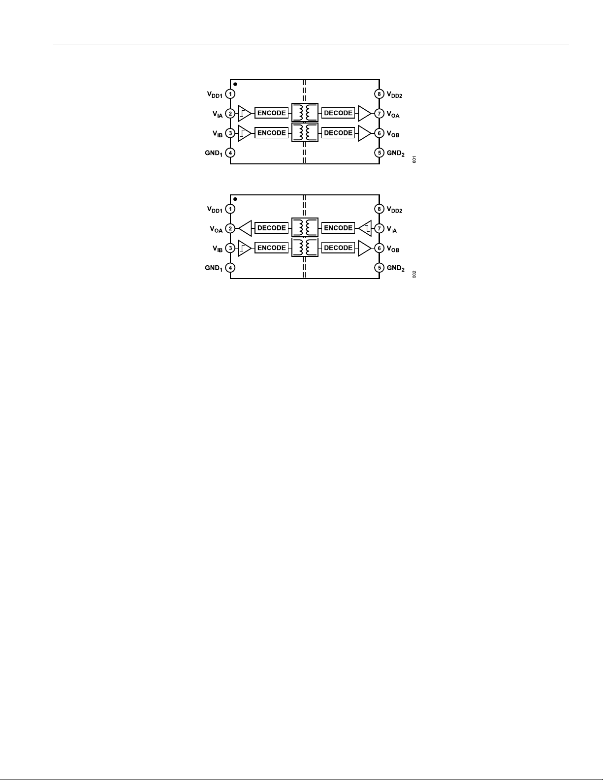
FUNCTIONAL BLOCK DIAGRAMS
Figure 1. ADuM1200 Functional Block Diagram
Figure 2. ADuM1201 Functional Block Diagram
analog.com Rev. L | 3 of 31
Page 4
Data Sheet ADuM1200/ADuM1201
SPECIFICATIONS
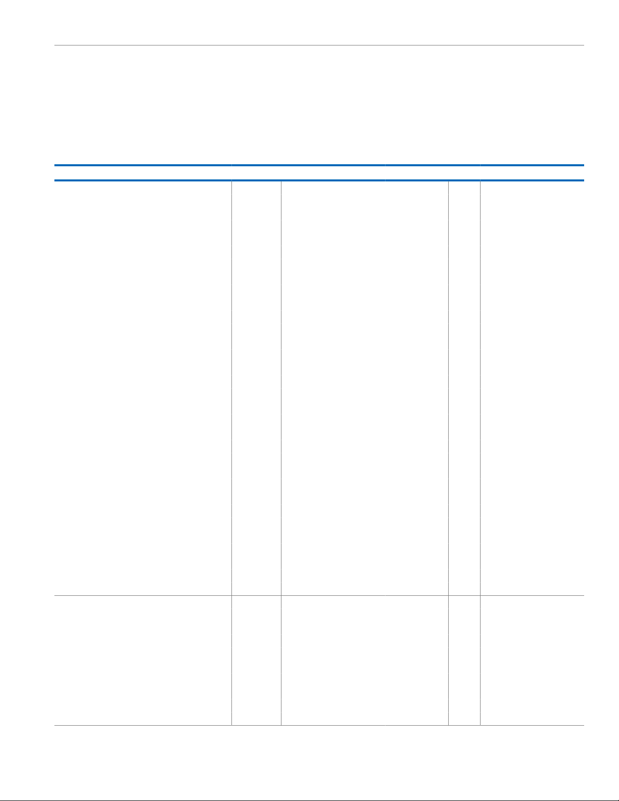
ELECTRICAL CHARACTERISTICS—5 V, 105°C OPERATION
All voltages are relative to the respective ground; 4.5 V ≤ V
the entire recommended operating range, unless otherwise noted; all typical specifications are at T
≤ 5.5 V, 4.5 V ≤ V
DD1
≤ 5.5 V; all minimum/maximum specifications apply over
DD2
= 25°C, V
A
DD1
= V
= 5 V; this does not
DD2
apply to the ADuM1200W and ADuM1201W automotive grade products.
Table 1.
Parameter Symbol Min Typ Max Unit Test Conditions/Comments
DC SPECIFICATIONS
Input Supply Current per Channel, Quiescent I
Output Supply Current per Channel, Quiescent I
ADuM1200 Total Supply Current, Two Channels
DDI (Q)
DDO (Q)
1
DC to 2 Mbps
V
Supply Current I
DD1
V
Supply Current I
DD2
DD1 (Q)
DD2 (Q)
10 Mbps (BR and CR Grades Only)
V
Supply Current I
DD1
V
Supply Current I
DD2
DD1 (10)
DD2 (10)
25 Mbps (CR Grade Only)
V
Supply Current I
DD1
V
Supply Current I
DD2
ADuM1201 Total Supply Current, Two Channels
DD1 (25)
DD2 (25)
1
DC to 2 Mbps
V
Supply Current I
DD1
V
Supply Current I
DD2
DD1 (Q)
DD2 (Q)
10 Mbps (BR and CR Grades Only)
V
Supply Current I
DD1
V
Supply Current I
DD2
DD1 (10)
DD2 (10)
25 Mbps (CR Grade Only)
V
Supply Current I
DD1
V
Supply Current I
DD2
DD1 (25)
DD2 (25)
For All Models
Input Currents IIA, I
Logic High Input Threshold V
Logic Low Input Threshold V
Logic High Output Voltages V
Logic Low Output Voltages V
IH
IL
OAH
OAL
IB
, V
, V
−10 +0.01 +10 µA 0 V ≤ VIA, VIB ≤ (V
0.7 (V
or V
DD1
or V
OBH(VDD1
(V
DD1
OBL
) − 0.1 5.0 V IOx = −20 µA, VIx = V
DD2
or V
) − 0.5 4.8 V IOx = −4 mA, VIx = V
DD2
SWITCHING SPECIFICATIONS
ADuM1200/ADuM1201AR CL = 15 pF, CMOS signal levels
Minimum Pulse Width
Maximum Data Rate
Propagation Delay
Pulse Width Distortion, |t
2
3
4
4
− t
|
PLH
PHL
PW 1000 ns
1 Mbps
t
PHL
, t
PLH
50 150 ns
PWD 40 ns
Change vs. Temperature 11 ps/°C
Propagation Delay Skew
Channel-to-Channel Matching
Output Rise/Fall Time (10% to 90%) tR/t
5
6
t
PSK
t
PSKCD/tPSKOD
F
0.50 0.60 mA
0.19 0.25 mA
1.1 1.4 mA DC to 1 MHz logic signal freq.
0.5 0.8 mA DC to 1 MHz logic signal freq.
4.3 5.5 mA 5 MHz logic signal freq.
1.3 2.0 mA 5 MHz logic signal freq.
10 13 mA 12.5 MHz logic signal freq.
2.8 3.4 mA 12.5 MHz logic signal freq.
0.8 1.1 mA DC to 1 MHz logic signal freq.
0.8 1.1 mA DC to 1 MHz logic signal freq.
2.8 3.5 mA 5 MHz logic signal freq.
2.8 3.5 mA 5 MHz logic signal freq.
6.3 8.0 mA 12.5 MHz logic signal freq.
6.3 8.0 mA 12.5 MHz logic signal freq.
) V
DD2
0.3 (V
or V
DD2
) V
DD1
0.0 0.1 V IOx = 20 µA, VIx = V
0.04 0.1 V IOx = 400 µA, VIx = V
0.2 0.4 V IOx = 4 mA, VIx = V
100 ns
50 ns
10 ns
DD1
IxL
IxL
or V
IxH
IxH
IxL
DD2
)
analog.com Rev. L | 4 of 31
Page 5
Data Sheet ADuM1200/ADuM1201
SPECIFICATIONS
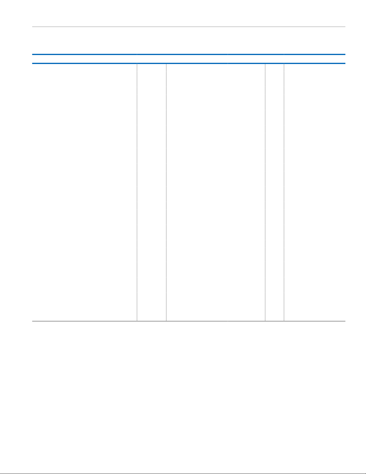
Table 1. (Continued)
Parameter Symbol Min Typ Max Unit Test Conditions/Comments
ADuM1200/ADuM1201BR
Minimum Pulse Width
Maximum Data Rate
Propagation Delay
Pulse Width Distortion, |t
Change vs. Temperature 5 ps/°C
Propagation Delay Skew
Channel-to-Channel Matching 3
Codirectional Channels
Opposing Directional Channels
Output Rise/Fall Time (10% to 90%) tR/t
ADuM1200/ADuM1201CR
Minimum Pulse Width
Maximum Data Rate
Propagation Delay
Pulse Width Distortion, |t
Change vs. Temperature 5 ps/°C
Propagation Delay Skew
Channel-to-Channel Matching 3 ns
Codirectional Channels
Opposing Directional Channels
Output Rise/Fall Time (10% to 90%) tR/t
For All Models
Common-Mode Transient Immunity
Logic High Output
Logic Low Output
Refresh Rate f
Dynamic Supply Current per Channel
Input I
Output I
2
3
4
4
− t
|
PLH
PHL
5
6
6
2
3
4
4
− t
|
PLH
PHL
5
6
6
7
PW 100 ns
10 Mbps
t
PHL
, t
PLH
20 50 ns
PWD 3 ns
t
PSK
t
PSKCD
t
PSKOD
F
2.5 ns
15 ns
ns
15 ns
PW 20 40 ns
25 50 Mbps
t
PHL
, t
PLH
20 45 ns
PWD 3 ns
t
PSK
t
PSKCD
t
PSKOD
F
2.5 ns
15 ns
15 ns
|CMH| 25 35 kV/µs VIx = V
DD1
or V
, VCM = 1000
DD2
V, transient magnitude = 800 V
7
|CML| 25 35 kV/µs
VIx = 0 V, VCM = 1000 V, transient magnitude = 800 V
8
r
DDI (D)
1.2 Mbps
0.19 mA/
Mbps
DDO (D)
0.05 mA/
Mbps
1
The supply current values are for both channels combined when running at identical data rates. Output supply current values are specified with no output load present. The
supply current associated with an individual channel operating at a given data rate can be calculated as described in the Power Consumption section. See Figure 6 through
Figure 8 for information on per-channel supply current as a function of data rate for unloaded and loaded conditions. See Figure 9 through Figure 11 for total V
DD1
and V
DD2
supply currents as a function of data rate for ADuM1200 and ADuM1201 channel configurations.
2
The minimum pulse width is the shortest pulse width at which the specified pulse width distortion is guaranteed.
3
The maximum data rate is the fastest data rate at which the specified pulse width distortion is guaranteed.
4
t
propagation delay is measured from the 50% level of the falling edge of the V
PHL
measured from the 50% level of the rising edge of the V
5
t
is the magnitude of the worst-case difference in t
PSK
signal to the 50% level of the rising edge of the V
Ix
and/or t
PHL
that is measured between units at the same operating temperature, supply voltages, and output load
PLH
signal to the 50% level of the falling edge of the V
Ix
signal.
Ox
signal. t
Ox
PLH
propagation delay is
within the recommended operating conditions.
6
Codirectional channel-to-channel matching is the absolute value of the difference in propagation delays between any two channels with inputs on the same side of the
isolation barrier. Opposing directional channel-to-channel matching is the absolute value of the difference in propagation delays between any two channels with inputs on
opposing sides of the isolation barrier.
analog.com Rev. L | 5 of 31
Page 6
Data Sheet ADuM1200/ADuM1201
SPECIFICATIONS
7
CMH is the maximum common-mode voltage slew rate that can be sustained while maintaining V
that can be sustained while maintaining V
< 0.8 V. The common-mode voltage slew rates apply to both rising and falling common-mode voltage edges. The transient
O
magnitude is the range over which the common mode is slewed.
8
Dynamic supply current is the incremental amount of supply current required for a 1 Mbps increase in the signal data rate. See Figure 6 through Figure 8 for information
on per-channel supply current as a function of data rate for unloaded and loaded conditions. See the Power Consumption section for guidance on calculating per-channel
supply current for a given data rate.
ELECTRICAL CHARACTERISTICS—3 V, 105°C OPERATION
> 0.8 V
O
. CML is the maximum common-mode voltage slew rate
DD2
All voltages are relative to the respective ground; 2.7 V ≤ V
the entire recommended operating range, unless otherwise noted; all typical specifications are at T
≤ 3.6 V, 2.7 V ≤ V
DD1
≤ 3.6 V; all minimum/maximum specifications apply over
DD2
= 25°C, V
A
DD1
= V
= 3.0 V; this does not
DD2
apply to ADuM1200W and ADuM1201W automotive grade products.
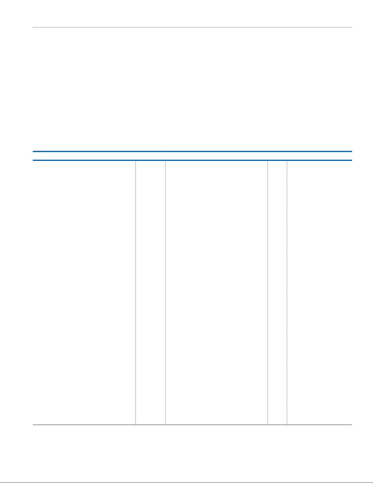
Table 2.
Parameter Symbol Min Typ Max Unit Test Conditions/Comments
DC SPECIFICATIONS
Input Supply Current per Channel, Quiescent I
Output Supply Current per Channel, Quiescent I
ADuM1200 Total Supply Current, Two Channels
1
DC to 2 Mbps
V
Supply Current I
DD1
V
Supply Current I
DD2
10 Mbps (BR and CR Grades Only)
V
Supply Current I
DD1
V
Supply Current I
DD2
25 Mbps (CR Grade Only)
V
Supply Current I
DD1
V
Supply Current I
DD2
ADuM1201 Total Supply Current, Two Channels
1
DC to 2 Mbps
V
Supply Current I
DD1
V
Supply Current I
DD2
10 Mbps (BR and CR Grades Only)
V
Supply Current I
DD1
V
Supply Current I
DD2
25 Mbps (CR Grade Only)
V
Supply Current I
DD1
V
Supply Current I
DD2
For All Models
Input Currents IIA, I
Logic High Input Threshold V
Logic Low Input Threshold V
Logic High Output Voltages V
Logic Low Output Voltages V
DDI (Q)
DDO (Q)
DD1 (Q)
DD2 (Q)
DD1 (10)
DD2 (10)
DD1 (25)
DD2 (25)
DD1 (Q)
DD2 (Q)
DD1 (10)
DD2 (10)
DD1 (25)
DD2 (25)
IB
IH
IL
, V
OAH
, V
OAL
−10 +0.01 +10
0.7 (V
or V
DD1
OBH(VDD1
or V
DD2
0.1
(V
or V
DD1
DD2
0.5
OBL
0.26 0.35 mA
0.11 0.20 mA
0.6 1.0 mA DC to 1 MHz logic signal freq.
0.2 0.6 mA DC to 1 MHz logic signal freq.
2.2 3.4 mA 5 MHz logic signal freq.
0.7 1.1 mA 5 MHz logic signal freq.
5.2 7.7 mA 12.5 MHz logic signal freq.
1.5 2.0 mA 12.5 MHz logic signal freq.
0.4 0.8 mA DC to 1 MHz logic signal freq.
0.4 0.8 mA DC to 1 MHz logic signal freq.
1.5 2.2 mA 5 MHz logic signal freq.
1.5 2.2 mA 5 MHz logic signal freq.
3.4 4.8 mA 12.5 MHz logic signal freq.
3.4 4.8 mA 12.5 MHz logic signal freq.
µA
) V
DD2
0.3 (V
or V
DD2
)
DD1
) −
3.0 V IOx = −20 µA, VIx = V
) −
2.8 V IOx = −4 mA, VIx = V
0.0 0.1 V IOx = 20 µA, VIx = V
0 V ≤ VIA, VIB ≤ (V
DD1
IxH
IxL
0.04 0.1 V IOx = 400 µA, VIx = V
0.2 0.4 V IOx = 4 mA, VIx = V
IxL
or V
IxH
IxL
DD2
)
analog.com Rev. L | 6 of 31
Page 7
Data Sheet ADuM1200/ADuM1201
SPECIFICATIONS
Table 2. (Continued)
Parameter Symbol Min Typ Max Unit Test Conditions/Comments
SWITCHING SPECIFICATIONS
ADuM1200/ADuM1201AR CL = 15 pF, CMOS signal levels
Minimum Pulse Width
Maximum Data Rate
Propagation Delay
Pulse Width Distortion, |t
Change vs. Temperature 11 ps/°C
Propagation Delay Skew
Channel-to-Channel Matching
Output Rise/Fall Time (10% to 90%) tR/t
ADuM1200/ADuM1201BR CL = 15 pF, CMOS signal levels
Minimum Pulse Width
Maximum Data Rate
Propagation Delay
Pulse Width Distortion, |t
Change vs. Temperature 5 ps/°C
Propagation Delay Skew
Channel-to-Channel Matching
Codirectional Channels
Opposing Directional Channels
Output Rise/Fall Time (10% to 90%) tR/t
ADuM1200/ADuM1201CR
Minimum Pulse Width
Maximum Data Rate
Propagation Delay
Pulse Width Distortion, |t
Change vs. Temperature 5 ps/°C
Propagation Delay Skew
Channel-to-Channel Matching
Codirectional Channels
Opposing Directional Channels
Output Rise/Fall Time (10% to 90%) tR/t
For All Models
Common-Mode Transient Immunity
Logic High Output
Logic Low Output
Refresh Rate f
Dynamic Supply Current per Channel
Input I
Output I
2
3
4
4
− t
|
PLH
PHL
5
6
2
3
4
4
− t
|
PLH
PHL
5
6
6
2
3
4
4
− t
|
PLH
PHL
5
6
6
7
PW 1000 ns
1 Mbps
t
PHL
, t
PLH
50 150 ns
PWD 40 ns
t
PSK
t
PSKCD/tPSKOD
F
10 ns
100 ns
50 ns
PW 100 ns
10 Mbps
t
PHL
, t
PLH
20 60 ns
PWD 3 ns
t
PSK
t
PSKCD
t
PSKOD
F
3.0 ns
22 ns
3 ns
22 ns
PW 20 40 ns
25 50 Mbps
t
PHL
, t
PLH
20 55 ns
PWD 3 ns
t
PSK
t
PSKCD
t
PSKOD
F
3.0 ns
16 ns
3 ns
16 ns
|CMH| 25 35 kV/µs VIx = V
DD1
or V
DD2
, VCM = 1000 V,
transient magnitude = 800 V
7
|CML| 25 35 kV/µs VIx = 0 V, VCM = 1000 V, transient
magnitude = 800 V
8
r
DDI (D)
1.1 Mbps
0.10 mA/
Mbps
DDO (D)
0.03 mA/
Mbps
1
The supply current values are for both channels combined when running at identical data rates. Output supply current values are specified with no output load present. The
supply current associated with an individual channel operating at a given data rate can be calculated as described in the Power Consumption section. See Figure 6 through
Figure 8 for information on per-channel supply current as a function of data rate for unloaded and loaded conditions. See Figure 9 through Figure 11 for total V
DD1
and V
DD2
supply currents as a function of data rate for ADuM1200 and ADuM1201 channel configurations.
analog.com Rev. L | 7 of 31
Page 8
Data Sheet ADuM1200/ADuM1201
SPECIFICATIONS
2
The minimum pulse width is the shortest pulse width at which the specified pulse width distortion is guaranteed.
3
The maximum data rate is the fastest data rate at which the specified pulse width distortion is guaranteed.
4
t
propagation delay is measured from the 50% level of the falling edge of the V
PHL
measured from the 50% level of the rising edge of the V
5
t
is the magnitude of the worst-case difference in t
PSK
signal to the 50% level of the rising edge of the V
Ix
and/or t
PHL
that is measured between units at the same operating temperature, supply voltages, and output load
PLH
within the recommended operating conditions.
6
Codirectional channel-to-channel matching is the absolute value of the difference in propagation delays between any two channels with inputs on the same side of the
isolation barrier. Opposing directional channel-to-channel matching is the absolute value of the difference in propagation delays between any two channels with inputs on
opposing sides of the isolation barrier.
7
CMH is the maximum common-mode voltage slew rate that can be sustained while maintaining V
that can be sustained while maintaining V
< 0.8 V. The common-mode voltage slew rates apply to both rising and falling common-mode voltage edges. The transient
O
magnitude is the range over which the common mode is slewed.
8
Dynamic supply current is the incremental amount of supply current required for a 1 Mbps increase in the signal data rate. See Figure 6 through Figure 8 for information
on per-channel supply current as a function of data rate for unloaded and loaded conditions. See the Power Consumption section for guidance on calculating per-channel
supply current for a given data rate.
ELECTRICAL CHARACTERISTICS—MIXED 5 V/3 V OR 3 V/5 V, 105°C OPERATION
signal to the 50% level of the falling edge of the V
Ix
signal.
Ox
> 0.8 V
O
. CML is the maximum common-mode voltage slew rate
DD2
signal. t
Ox
propagation delay is
PLH
All voltages are relative to the respective ground; 5 V/3 V operation: 4.5 V ≤ V
V
≤ 3.6 V, 4.5 V ≤ V
DD1
noted; all typical specifications are at T
≤ 5.5 V; all minimum/maximum specifications apply over the entire recommended operating range, unless otherwise
DD2
= 25°C; V
A
= 3.0 V, V
DD1
= 5.0 V; or V
DD2
≤ 5.5 V, 2.7 V ≤ V
DD1
= 5.0 V, V
DD1
≤ 3.6 V. 3 V/5 V operation: 2.7 V ≤
DD2
= 3.0 V; this does not apply to ADuM1200W
DD2
and ADuM1201W automotive grade products.
Table 3.
Parameter Symbol Min Typ Max Unit Test Conditions /Comments
DC SPECIFICATIONS
Input Supply Current per Channel,
Quiescent
5 V/3 V Operation 0.50 0.6 mA
3 V/5 V Operation 0.26 0.35 mA
Output Supply Current per Channel,
Quiescent
5 V/3 V Operation 0.11 0.20 mA
3 V/5 V Operation 0.19 0.25 mA
ADuM1200 Total Supply Current, Two
1
Channels
DC to 2 Mbps
V
Supply Current I
DD1
5 V/3 V Operation 1.1 1.4 mA DC to 1 MHz logic signal freq.
3 V/5 V Operation 0.6 1.0 mA DC to 1 MHz logic signal freq.
V
Supply Current I
DD2
5 V/3 V Operation 0.2 0.6 mA DC to 1 MHz logic signal freq.
3 V/5 V Operation 0.5 0.8 mA DC to 1 MHz logic signal freq.
10 Mbps (BR and CR Grades Only)
V
Supply Current I
DD1
5 V/3 V Operation 4.3 5.5 mA 5 MHz logic signal freq.
3 V/5 V Operation 2.2 3.4 mA 5 MHz logic signal freq.
V
Supply Current I
DD2
5 V/3 V Operation 0.7 1.1 mA 5 MHz logic signal freq.
3 V/5 V Operation 1.3 2.0 mA 5 MHz logic signal freq.
I
DDI (Q)
I
DDO (Q)
DD1 (Q)
DD2 (Q)
DD1 (10)
DD2 (10)
analog.com Rev. L | 8 of 31
Page 9
Data Sheet ADuM1200/ADuM1201
SPECIFICATIONS
Table 3. (Continued)
Parameter Symbol Min Typ Max Unit Test Conditions /Comments
25 Mbps (CR Grade Only)
V
Supply Current I
DD1
5 V/3 V Operation 10 13 mA 12.5 MHz logic signal freq.
3 V/5 V Operation 5.2 7.7 mA 12.5 MHz logic signal freq.
V
Supply Current I
DD2
5 V/3 V Operation 1.5 2.0 mA 12.5 MHz logic signal freq.
3 V/5 V Operation 2.8 3.4 mA 12.5 MHz logic signal freq.
ADuM1201 Total Supply Current, Two
1
Channels
DC to 2 Mbps
V
Supply Current I
DD1
5 V/3 V Operation 0.8 1.1 mA DC to 1 MHz logic signal freq.
3 V/5 V Operation 0.4 0.8 mA DC to 1 MHz logic signal freq.
V
Supply Current I
DD2
5 V/3 V Operation 0.4 0.8 mA DC to 1 MHz logic signal freq.
3 V/5 V Operation 0.8 1.1 mA DC to 1 MHz logic signal freq.
10 Mbps (BR and CR Grades Only)
V
Supply Current I
DD1
5 V/3 V Operation 2.8 3.5 mA 5 MHz logic signal freq.
3 V/5 V Operation 1.5 2.2 mA 5 MHz logic signal freq.
V
Supply Current I
DD2
5 V/3 V Operation 1.5 2.2 mA 5 MHz logic signal freq.
3 V/5 V Operation 2.8 3.5 mA 5 MHz logic signal freq.
25 Mbps (CR Grade Only)
V
Supply Current I
DD1
5 V/3 V Operation 6.3 8.0 mA 12.5 MHz logic signal freq.
3 V/5 V Operation 3.4 4.8 mA 12.5 MHz logic signal freq.
V
Supply Current I
DD2
5 V/3 V Operation 3.4 4.8 mA 12.5 MHz logic signal freq.
3 V/5 V Operation 6.3 8.0 mA 12.5 MHz logic signal freq.
For All Models
Input Currents IIA, I
Logic High Input Threshold V
Logic Low Input Threshold V
Logic High Output Voltages V
Logic Low Output Voltages V
SWITCHING SPECIFICATIONS
ADuM1200/ADuM1201AR CL = 15 pF, CMOS signal levels
Minimum Pulse Width
Maximum Data Rate
Propagation Delay
Pulse Width Distortion, |t
2
3
4
− t
PLH
PHL
Change vs. Temperature 11 ps/°C
Propagation Delay Skew
5
DD1 (25)
DD2 (25)
DD1 (Q)
DD2 (Q)
DD1 (10)
DD2 (10)
DD1 (25)
DD2 (25)
−10 +0.01 +10 µA 0 V ≤ VIA, VIB ≤ (V
0.7 (V
or V
DD1
) V
DD2
0.3 (V
or V
) −
V
OBH(VDD1
DD2
DD1
or V
DD2
IH
IL
OAH
IB
, V
0.1
(V
or V
) −
(V
or V
DD2
) −
OAL
, V
OBL
0.5
DD1
DD2
DD1
0.2
0.0 0.1 V IOx = 20 µA, VIx = V
0.04 0.1 V IOx = 400 µA, VIx = V
0.2 0.4 V IOx = 4 mA, VIx = V
PW 1000 ns
1 Mbps
t
, t
PHL
4
|
PLH
PWD 40 ns
t
PSK
50 150 ns
50 ns
DD1
or V
) V
DD2
V IOx = −20 µA, VIx = V
V IOx = −4 mA, VIx = V
DD1
IxL
IxL
or V
IxH
IxH
IxL
DD2
)
analog.com Rev. L | 9 of 31
Page 10
Data Sheet ADuM1200/ADuM1201
SPECIFICATIONS
Table 3. (Continued)
Parameter Symbol Min Typ Max Unit Test Conditions /Comments
Channel-to-Channel Matching6t
Output Rise/Fall Time (10% to 90%) tR/t
PSKCD/tPSKOD
F
10 ns
ADuM1200/ADuM1201BR CL = 15 pF, CMOS signal levels
Minimum Pulse Width
Maximum Data Rate
Propagation Delay
Pulse Width Distortion, |t
2
3
4
− t
PLH
PHL
PW 100 ns
10 Mbps
t
, t
PHL
4
|
PLH
PWD 3 ns
15 55 ns
Change vs. Temperature 5 ps/°C
Propagation Delay Skew
5
t
PSK
Channel-to-Channel Matching
Codirectional Channels
Opposing Directional Channels6t
Output Rise/Fall Time (10% to 90%) tR/t
6
t
PSKCD
PSKOD
F
5 V/3 V Operation 3.0 ns
3 V/5 V Operation 2.5 ns
ADuM1200/ADuM1201CR CL = 15 pF, CMOS signal levels
Minimum Pulse Width
Maximum Data Rate
Propagation Delay
Pulse Width Distortion, |t
2
3
4
− t
PLH
PHL
PW 20 40 ns
25 50 Mbps
t
, t
PHL
4
|
PLH
PWD 3 ns
20 50 ns
Change vs. Temperature 5 ps/°C
Propagation Delay Skew
5
t
PSK
Channel-to-Channel Matching
Codirectional Channels
Opposing Directional Channels6t
Output Rise/Fall Time (10% to 90%) tR/t
6
t
PSKCD
PSKOD
F
5 V/3 V Operation 3.0 ns
3 V/5 V Operation 2.5 ns
For All Models
Common-Mode Transient Immunity
Logic High Output
Logic Low Output
Refresh Rate f
7
7
|CMH| 25 35 kV/µs VIx = V
|CML| 25 35 kV/µs VIx = 0 V, VCM = 1000 V, transient
r
5 V/3 V Operation 1.2 Mbps
3 V/5 V Operation 1.1 Mbps
Input Dynamic Supply Current per
8
Channel
I
DDI (D)
5 V/3 V Operation 0.19 mA/
3 V/5 V Operation 0.10 mA/
Output Dynamic Supply Current per
8
Channel
I
DDO (D)
5 V/3 V Operation 0.03 mA/
3 V/5 V Operation 0.05 mA/
50 ns
22 ns
3 ns
22 ns
15 ns
3 ns
15 ns
Mbps
Mbps
Mbps
Mbps
or V
DD1
, VCM = 1000 V,
DD2
transient magnitude = 800 V
magnitude = 800 V
analog.com Rev. L | 10 of 31
Page 11

Data Sheet ADuM1200/ADuM1201
SPECIFICATIONS
1
The supply current values are for both channels combined when running at identical data rates. Output supply current values are specified with no output load present. The
supply current associated with an individual channel operating at a given data rate can be calculated as described in the Power Consumption section. See Figure 6 through
Figure 8 for information on per-channel supply current as a function of data rate for unloaded and loaded conditions. See Figure 9 through Figure 11 for total V
supply currents as a function of data rate for ADuM1200 and ADuM1201 channel configurations.
2
The minimum pulse width is the shortest pulse width at which the specified pulse width distortion is guaranteed.
3
The maximum data rate is the fastest data rate at which the specified pulse width distortion is guaranteed.
4
t
propagation delay is measured from the 50% level of the falling edge of the V
PHL
measured from the 50% level of the rising edge of the V
5
t
is the magnitude of the worst-case difference in t
PSK
signal to the 50% level of the rising edge of the V
Ix
and/or t
PHL
that is measured between units at the same operating temperature, supply voltages, and output load
PLH
signal to the 50% level of the falling edge of the V
Ix
signal.
Ox
signal. t
Ox
propagation delay is
PLH
within the recommended operating conditions.
6
Codirectional channel-to-channel matching is the absolute value of the difference in propagation delays between any two channels with inputs on the same side of the
isolation barrier. Opposing directional channel-to-channel matching is the absolute value of the difference in propagation delays between any two channels with inputs on
opposing sides of the isolation barrier.
7
CMH is the maximum common-mode voltage slew rate that can be sustained while maintaining V
that can be sustained while maintaining V
< 0.8 V. The common-mode voltage slew rates apply to both rising and falling common-mode voltage edges. The transient
O
> 0.8 V
O
. CML is the maximum common-mode voltage slew rate
DD2
magnitude is the range over which the common mode is slewed.
8
Dynamic supply current is the incremental amount of supply current required for a 1 Mbps increase in the signal data rate. See Figure 6 through Figure 8 for information
on per-channel supply current as a function of data rate for unloaded and loaded conditions. See the Power Consumption section for guidance on calculating per-channel
supply current for a given data rate.
DD1
and V
DD2
ELECTRICAL CHARACTERISTICS—5 V, 125°C OPERATION
All voltages are relative to the respective ground; 4.5 V ≤ V
the entire recommended operating range, unless otherwise noted; all typical specifications are at T
≤ 5.5 V, 4.5 V ≤ V
DD1
≤ 5.5 V; all minimum/maximum specifications apply over
DD2
= 25°C, V
A
DD1
= V
= 5 V; this applies to
DD2
ADuM1200W and ADuM1201W automotive grade products.
Table 4.
Parameter Symbol Min Typ Max Unit Test Conditions/Comments
DC SPECIFICATIONS
Input Supply Current per Channel, Quiescent I
Output Supply Current per Channel,
Quiescent
ADuM1200W, Total Supply Current, Two
1
Channels
DC to 2 Mbps
V
Supply Current I
DD1
V
Supply Current I
DD2
10 Mbps (TRZ and URZ Grades Only)
V
Supply Current I
DD1
V
Supply Current I
DD2
25 Mbps (URZ Grade Only)
V
Supply Current I
DD1
V
Supply Current I
DD2
ADuM1201W, Total Supply Current, Two
1
Channels
DC to 2 Mbps
V
Supply Current I
DD1
V
Supply Current I
DD2
10 Mbps (TRZ and URZ Grades Only)
V
Supply Current I
DD1
V
Supply Current I
DD2
DDI (Q)
I
DDO (Q)
DD1 (Q)
DD2 (Q)
DD1 (10)
DD2 (10)
DD1 (25)
DD2 (25)
DD1 (Q)
DD2 (Q)
DD1 (10)
DD2 (10)
0.50 0.60 mA
0.19 0.25 mA
1.1 1.4 mA DC to 1 MHz logic signal freq.
0.5 0.8 mA DC to 1 MHz logic signal freq.
4.3 5.5 mA 5 MHz logic signal freq.
1.3 2.0 mA 5 MHz logic signal freq.
10 13 mA 12.5 MHz logic signal freq.
2.8 3.4 mA 12.5 MHz logic signal freq.
0.8 1.1 mA DC to 1 MHz logic signal freq.
0.8 1.1 mA DC to 1 MHz logic signal freq.
2.8 3.5 mA 5 MHz logic signal freq.
2.8 3.5 mA 5 MHz logic signal freq.
analog.com Rev. L | 11 of 31
Page 12
Data Sheet ADuM1200/ADuM1201
SPECIFICATIONS
Table 4. (Continued)
Parameter Symbol Min Typ Max Unit Test Conditions/Comments
25 Mbps (URZ Grade Only)
V
Supply Current I
DD1
V
Supply Current I
DD2
DD1 (25)
DD2 (25)
For All Models
Input Currents IIA, I
Logic High Input Threshold V
Logic Low Input Threshold V
Logic High Output Voltages V
Logic Low Output Voltages V
IH
IL
OAH
OAL
IB
, V
, V
−10 +0.01 +10 µA 0 V ≤ VIA, VIB ≤ (V
0.7 (V
or V
DD1
(V
DD1
or V
or V
DD2
DD2
OBH(VDD1
OBL
SWITCHING SPECIFICATIONS
ADuM1200/ADuM1201WSRZ CL = 15 pF, CMOS signal levels
Minimum Pulse Width
Maximum Data Rate
Propagation Delay
Pulse Width Distortion, |t
Propagation Delay Skew
Channel-to-Channel Matching6t
Output Rise/Fall Time (10% to 90%) tR/t
2
3
4
4
− t
|
PLH
PHL
5
PW 1000 ns
1 Mbps
t
PHL
, t
PLH
20 150 ns
PWD 40 ns
t
PSK
PSKCD/tPSKOD
F
ADuM1200/ADuM1201WTRZ CL = 15 pF, CMOS signal levels
Minimum Pulse Width
Maximum Data Rate
Propagation Delay
Pulse Width Distortion, |t
2
3
4
4
− t
|
PLH
PHL
PW 100 ns
10 Mbps
t
PHL
, t
PLH
20 50 ns
PWD 3 ns
Change vs. Temperature 5 ps/°C
Propagation Delay Skew
5
t
PSK
Channel-to-Channel Matching
Codirectional Channels
Opposing Directional Channels6t
Output Rise/Fall Time (10% to 90%) tR/t
6
t
PSKCD
PSKOD
F
ADuM1200/ADuM1201WURZ CL = 15 pF, CMOS signal levels
Minimum Pulse Width
Maximum Data Rate
Propagation Delay
Pulse Width Distortion, |t
2
3
4
4
− t
|
PLH
PHL
PW 20 40 ns
25 50 Mbps
t
PHL
, t
PLH
20 45 ns
PWD 3 ns
Change vs. Temperature 5 ps/°C
Propagation Delay Skew
5
t
PSK
Channel-to-Channel Matching
Codirectional Channels
Opposing Directional Channels6t
Output Rise/Fall Time (10% to 90%) tR/t
6
t
PSKCD
PSKOD
F
For All Models
Common-Mode Transient Immunity
Logic High Output
7
|CMH| 25 35 kV/µs VIx = V
6.3 8.0 mA 12.5 MHz logic signal freq.
6.3 8.0 mA 12.5 MHz logic signal freq.
DD1
) V
DD2
0.3 (V
or V
DD2
) V
DD1
) − 0.1 5.0 V IOx = −20 µA, VIx = V
) − 0.5 4.8 V IOx = −4 mA, VIx = V
0.0 0.1 V IOx = 20 µA, VIx = V
0.04 0.1 V IOx = 400 µA, VIx = V
0.2 0.4 V IOx = 4 mA, VIx = V
IxL
100 ns
50 ns
2.5 ns
15 ns
3 ns
15 ns
2.5 ns
15 ns
3 ns
15 ns
2.5 ns
, V
, VCM = 1000 V,
DD1
DD2
transient magnitude = 800 V
IxH
IxH
IxL
IxL
or V
DD2
)
analog.com Rev. L | 12 of 31
Page 13
Data Sheet ADuM1200/ADuM1201
SPECIFICATIONS
Table 4. (Continued)
Parameter Symbol Min Typ Max Unit Test Conditions/Comments
Logic Low Output
Refresh Rate f
Dynamic Supply Current per Channel
Input I
Output I
1
The supply current values are for both channels combined when running at identical data rates. Output supply current values are specified with no output load present. The
supply current associated with an individual channel operating at a given data rate can be calculated as described in the Power Consumption section. See Figure 6 through
Figure 8 for information on per-channel supply current as a function of data rate for unloaded and loaded conditions. See Figure 9 through Figure 11 for total I
supply currents as a function of data rate for ADuM1200W and ADuM1201W channel configurations.
2
The minimum pulse width is the shortest pulse width at which the specified pulse width distortion is guaranteed.
3
The maximum data rate is the fastest data rate at which the specified pulse width distortion is guaranteed.
4
t
propagation delay is measured from the 50% level of the falling edge of the V
PHL
measured from the 50% level of the rising edge of the V
5
t
is the magnitude of the worst-case difference in t
PSK
within the recommended operating conditions.
6
Codirectional channel-to-channel matching is the absolute value of the difference in propagation delays between any two channels with inputs on the same side of the
isolation barrier. Opposing directional channel-to-channel matching is the absolute value of the difference in propagation delays between any two channels with inputs on
opposing sides of the isolation barrier.
7
CMH is the maximum common-mode voltage slew rate that can be sustained while maintaining V
that can be sustained while maintaining V
magnitude is the range over which the common mode is slewed.
8
Dynamic supply current is the incremental amount of supply current required for a 1 Mbps increase in the signal data rate. See Figure 6 through Figure 8 for information
on per-channel supply current as a function of data rate for unloaded and loaded conditions. See the Power Consumption section for guidance on calculating per-channel
supply current for a given data rate.
7
|CML| 25 35 kV/µs VIx = 0 V, VCM = 1000 V,
transient magnitude = 800 V
r
8
DDI (D)
1.2 Mbps
0.19 mA/
Mbps
DDO (D)
0.05 mA/
Mbps
and I
DD1
DD2
signal to the 50% level of the falling edge of the V
Ix
signal to the 50% level of the rising edge of the V
Ix
and/or t
PHL
< 0.8 V. The common-mode voltage slew rates apply to both rising and falling common-mode voltage edges. The transient
O
that is measured between units at the same operating temperature, supply voltages, and output load
PLH
> 0.8 V
O
signal.
Ox
. CML is the maximum common-mode voltage slew rate
DD2
signal. t
Ox
propagation delay is
PLH
ELECTRICAL CHARACTERISTICS—3 V, 125°C OPERATION
All voltages are relative to the respective ground; 3.0 V ≤ V
the entire recommended operating range, unless otherwise noted; all typical specifications are at T
≤ 3.6 V, 3.0 V ≤ V
DD1
≤ 3.6 V. All minimum/maximum specifications apply over
DD2
= 25°C, V
A
DD1
= V
= 3.0 V; this applies
DD2
to ADuM1200W and ADuM1201W automotive grade products.
Table 5.
Parameter Symbol Min Typ Max Unit Test Conditions/Comments
DC SPECIFICATIONS
Input Supply Current per Channel, Quiescent I
Output Supply Current per Channel, Quiescent I
ADuM1200W, Total Supply Current, Two
1
Channels
DDI (Q)
DDO (Q)
DC to 2 Mbps
V
Supply Current I
DD1
V
Supply Current I
DD2
DD1 (Q)
DD2 (Q)
10 Mbps (TRZ and URZ Grades Only)
V
Supply Current I
DD1
V
Supply Current I
DD2
DD1 (10)
DD2 (10)
25 Mbps (URZ Grade Only)
V
Supply Current I
DD1
DD1 (25)
analog.com Rev. L | 13 of 31
0.26 0.35 mA
0.11 0.20 mA
0.6 1.0 mA DC to 1 MHz logic signal freq.
0.2 0.6 mA DC to 1 MHz logic signal freq.
2.2 3.4 mA 5 MHz logic signal freq.
0.7 1.1 mA 5 MHz logic signal freq.
5.2 7.7 mA 12.5 MHz logic signal freq.
Page 14
Data Sheet ADuM1200/ADuM1201
SPECIFICATIONS
Table 5. (Continued)
Parameter Symbol Min Typ Max Unit Test Conditions/Comments
V
Supply Current I
DD2
ADuM1201W, Total Supply Current, Two
1
Channels
DD2 (25)
DC to 2 Mbps
V
Supply Current I
DD1
V
Supply Current I
DD2
DD1 (Q)
DD2 (Q)
10 Mbps (TRZ and URZ Grades Only)
V
Supply Current I
DD1
V
Supply Current I
DD2
DD1 (10)
DD2 (10)
25 Mbps (URZ Grade Only)
V
Supply Current I
DD1
V
Supply Current I
DD2
DD1 (25)
DD2 (25)
For All Models
Input Currents IIA, I
Logic High Input Threshold V
Logic Low Input Threshold V
Logic High Output Voltages V
Logic Low Output Voltages V
IH
IL
OAH
OAL
IB
, V
, V
−10 +0.01 +10 µA 0 V ≤ VIA, VIB ≤ (V
0.7 (V
or V
DD1
DD2
or V
OBH(VDD1
(V
DD1
OBL
) − 0.1 3.0 V IOx = −20 µA, VIx = V
DD2
or V
) − 0.5 2.8 V IOx = −4 mA, VIx = V
DD2
SWITCHING SPECIFICATIONS
ADuM1200/ADuM1201WSRZ CL = 15 pF, CMOS signal levels
Minimum Pulse Width
Maximum Data Rate
Propagation Delay
Pulse Width Distortion, |t
Propagation Delay Skew
Channel-to-Channel Matching
Output Rise/Fall Time (10% to 90%) tR/t
2
3
4
4
− t
|
PLH
PHL
5
6
PW 1000 ns
1 Mbps
t
PHL
, t
PLH
20 150 ns
PWD 40 ns
t
PSK
t
PSKCD/tPSKOD
F
ADuM1200/ADuM1201WTRZ CL = 15 pF, CMOS signal levels
Minimum Pulse Width
Maximum Data Rate
Propagation Delay
Pulse Width Distortion, |t
2
3
4
4
− t
|
PLH
PHL
PW 100 ns
10 Mbps
t
PHL
, t
PLH
20 60 ns
PWD 3 ns
Change vs. Temperature 5 ps/°C
Propagation Delay Skew
5
t
PSK
Channel-to-Channel Matching
Codirectional Channels
Opposing Directional Channels6t
Output Rise/Fall Time (10% to 90%) tR/t
6
t
PSKCD
PSKOD
F
ADuM1200/ADuM1201WCR CL = 15 pF, CMOS signal levels
Minimum Pulse Width
Maximum Data Rate
Propagation Delay
Pulse Width Distortion, |t
2
3
4
4
− t
|
PLH
PHL
PW 20 40 ns
25 50 Mbps
t
PHL
, t
PLH
20 55 ns
PWD 3 ns
Change vs. Temperature 5 ps/°C
Propagation Delay Skew
5
t
PSK
1.5 2.0 mA 12.5 MHz logic signal freq.
0.4 0.8 mA DC to 1 MHz logic signal freq.
0.4 0.8 mA DC to 1 MHz logic signal freq.
1.5 2.2 mA 5 MHz logic signal freq.
1.5 2.2 mA 5 MHz logic signal freq.
3.4 4.8 mA 12.5 MHz logic signal freq.
3.4 4.8 mA 12.5 MHz logic signal freq.
or V
DD1
) V
0.3 (V
or V
DD2
)
IxH
IxH
IxL
IxL
IxL
DD1
0.0 0.1 V IOx = 20 µA, VIx = V
0.04 0.1 V IOx = 400 µA, VIx = V
0.2 0.4 V IOx = 4 mA, VIx = V
100 ns
50 ns
3 ns
22 ns
3 ns
22 ns
3.0 ns
16 ns
DD2
)
analog.com Rev. L | 14 of 31
Page 15

Data Sheet ADuM1200/ADuM1201
SPECIFICATIONS
Table 5. (Continued)
Parameter Symbol Min Typ Max Unit Test Conditions/Comments
Channel-to-Channel Matching
Codirectional Channels
Opposing Directional Channels6t
Output Rise/Fall Time (10% to 90%) tR/t
For All Models
Common-Mode Transient Immunity
Logic High Output
Logic Low Output
Refresh Rate f
Dynamic Supply Current per Channel
Input I
Output I
1
The supply current values are for both channels combined when running at identical data rates. Output supply current values are specified with no output load present. The
supply current associated with an individual channel operating at a given data rate can be calculated as described in the Power Consumption section. See Figure 6 through
Figure 8 for information on per-channel supply current as a function of data rate for unloaded and loaded conditions. See Figure 9 through Figure 11 for total I
supply currents as a function of data rate for ADuM1200W and ADuM1201W channel configurations.
2
The minimum pulse width is the shortest pulse width at which the specified pulse width distortion is guaranteed.
3
The maximum data rate is the fastest data rate at which the specified pulse width distortion is guaranteed.
4
t
propagation delay is measured from the 50% level of the falling edge of the V
PHL
measured from the 50% level of the rising edge of the V
5
t
is the magnitude of the worst-case difference in t
PSK
within the recommended operating conditions.
6
Codirectional channel-to-channel matching is the absolute value of the difference in propagation delays between any two channels with inputs on the same side of the
isolation barrier. Opposing directional channel-to-channel matching is the absolute value of the difference in propagation delays between any two channels with inputs on
opposing sides of the isolation barrier.
7
CMH is the maximum common-mode voltage slew rate that can be sustained while maintaining V
that can be sustained while maintaining V
magnitude is the range over which the common mode is slewed.
8
Dynamic supply current is the incremental amount of supply current required for a 1 Mbps increase in the signal data rate. See Figure 6 through Figure 8 for information
on per-channel supply current as a function of data rate for unloaded and loaded conditions. See the Power Consumption section for guidance on calculating per-channel
supply current for a given data rate.
6
7
t
PSKCD
PSKOD
F
3.0 ns
3 ns
16 ns
|CMH| 25 35 kV/µs VIx = V
DD1
, V
, VCM = 1000
DD2
V,transient magnitude = 800 V
7
|CML| 25 35 kV/µs VIx = 0 V, VCM = 1000 V, transient
magnitude = 800 V
8
r
DDI (D)
1.1 Mbps
0.10 mA/
Mbps
DDO (D)
0.03 mA/
Mbps
and I
DD1
DD2
signal to the 50% level of the falling edge of the V
Ix
signal to the 50% level of the rising edge of the V
Ix
and/or t
PHL
< 0.8 V. The common-mode voltage slew rates apply to both rising and falling common-mode voltage edges. The transient
O
that is measured between units at the same operating temperature, supply voltages, and output load
PLH
> 0.8 V
O
signal.
Ox
. CML is the maximum common-mode voltage slew rate
DD2
signal. t
Ox
propagation delay is
PLH
analog.com Rev. L | 15 of 31
Page 16
Data Sheet ADuM1200/ADuM1201
SPECIFICATIONS
ELECTRICAL CHARACTERISTICS—MIXED 5 V/3 V, 125°C OPERATION
All voltages are relative to the respective ground; 5 V/3 V operation: 4.5 V ≤ V
≤ 5.5 V, 3.0 V ≤ V
DD1
≤ 3.6 V. 3 V/5 V operation; all
DD2
minimum/maximum specifications apply over the entire recommended operating range, unless otherwise noted; all typical specifications are at
TA = 25°C; V
Table 6.
Parameter Symbol Min Typ Max Unit Test Conditions/Comments
DC SPECIFICATIONS
Input Supply Current per Channel,
Quiescent
Output Supply Current per Channel,
Quiescent
ADuM1200W, Total Supply Current, Two
Channels
DC to 2 Mbps
V
V
10 Mbps (TRZ and URZ Grades Only)
V
V
25 Mbps (URZ Grade Only)
V
V
ADuM1201W, Total Supply Current, Two
Channels
DC to 2 Mbps
V
V
10 Mbps (TRZ and URZ Grades Only)
V
V
25 Mbps (URZ Grade Only)
V
V
For All Models
Input Currents IIA, I
Logic High Input Threshold V
Logic Low Input Threshold V
Logic High Output Voltages V
Logic Low Output Voltages V
SWITCHING SPECIFICATIONS
ADuM1200/ADuM1201WSRZ CL = 15 pF, CMOS signal levels
Minimum Pulse Width
Maximum Data Rate
Propagation Delay
Pulse Width Distortion, |t
= 5.0 V, V
DD1
1
Supply Current I
DD1
Supply Current I
DD2
Supply Current I
DD1
Supply Current I
DD2
Supply Current I
DD1
Supply Current I
DD2
1
Supply Current I
DD1
Supply Current I
DD2
Supply Current I
DD1
Supply Current I
DD2
Supply Current I
DD1
Supply Current I
DD2
3
4
= 3.0 V; this applies to ADuM1200W and ADuM1201W automotive grade products.
DD2
2
− t
PLH
PHL
I
DDI (Q)
I
DDO (Q)
DD1 (Q)
DD2 (Q)
DD1 (10)
DD2 (10)
DD1 (25)
DD2 (25)
DD1 (Q)
DD2 (Q)
DD1 (10)
DD2 (10)
DD1 (25)
DD2 (25)
IB
IH
IL
, V
OAH
−10 +0.01 +10 µA 0 V ≤ VIA, VIB ≤ (V
0.7 (V
or V
DD1
(V
DD1
or V
or V
DD2
DD2
OBH(VDD1
0.50 0.6 mA
0.11 0.20 mA
1.1 1.4 mA DC to 1 MHz logic signal freq.
0.2 0.6 mA DC to 1 MHz logic signal freq.
4.3 5.5 mA 5 MHz logic signal freq.
0.7 1.1 mA 5 MHz logic signal freq.
10 13 mA 12.5 MHz logic signal freq.
1.5 2.0 mA 12.5 MHz logic signal freq.
0.8 1.1 mA DC to 1 MHz logic signal freq.
0.4 0.8 mA DC to 1 MHz logic signal freq.
2.8 3.5 mA 5 MHz logic signal freq.
1.5 2.2 mA 5 MHz logic signal freq.
6.3 8.0 mA 12.5 MHz logic signal freq.
3.4 4.8 mA 12.5 MHz logic signal freq.
) V
DD2
0.3 (V
V
DD2
) − 0.1 V
) − 0.5 (V
DD1
DD1
or V
or V
DD2
DD2
) −
0.2
OAL
, V
OBL
0.0 0.1 V IOx = 20 µA, VIx = V
0.04 0.1 V IOx = 400 µA, VIx = V
0.2 0.4 V IOx = 4 mA, VIx = V
PW 1000 ns
1 Mbps
t
, t
PHL
4
|
PLH
PWD 40 ns
15 150 ns
)
DD1
or
V
V IOx = −20 µA, VIx = V
V IOx = −4 mA, VIx = V
DD1
IxH
IxL
IxL
or V
IxH
IxL
DD2
)
analog.com Rev. L | 16 of 31
Page 17

Data Sheet ADuM1200/ADuM1201
SPECIFICATIONS
Table 6. (Continued)
Parameter Symbol Min Typ Max Unit Test Conditions/Comments
Propagation Delay Skew
Channel-to-Channel Matching6t
Output Rise/Fall Time (10% to 90%) tR/t
ADuM1200/ADuM1201WTRZ CL = 15 pF, CMOS signal levels
Minimum Pulse Width
Maximum Data Rate
Propagation Delay
Pulse Width Distortion, |t
Change vs. Temperature 5 ps/°C
Propagation Delay Skew
Channel-to-Channel Matching
Codirectional Channels
Opposing Directional Channels6t
Output Rise/Fall Time (10% to 90%) tR/t
ADuM1200/ADuM1201WURZ CL = 15 pF, CMOS signal levels
Minimum Pulse Width
Maximum Data Rate
Propagation Delay
Pulse Width Distortion, |t
Change vs. Temperature 5 ps/°C
Propagation Delay Skew
Channel-to-Channel Matching
Codirectional Channels
Opposing Directional Channels6t
Output Rise/Fall Time (10% to 90%) tR/t
For All Models
Common-Mode Transient Immunity
Logic High Output
Logic Low Output
Refresh Rate f
Dynamic Supply Current per Channel
Input I
Output I
5
2
3
4
− t
PLH
PHL
5
6
2
3
4
− t
PLH
PHL
5
6
7
t
PSK
PSKCD/
t
PSKOD
F
3 ns
50 ns
50 ns
PW 100 ns
10 Mbps
t
, t
PHL
4
|
PLH
PWD 3 ns
t
PSK
t
PSKCD
PSKOD
F
15 55 ns
22 ns
3 ns
22 ns
3.0 ns
PW 20 40 ns
25 50 Mbps
t
, t
PHL
4
|
PLH
PWD 3 ns
t
PSK
t
PSKCD
PSKOD
F
20 50 ns
15 ns
3 ns
15 ns
3.0 ns
|CMH| 25 35 kV/µs VIx = V
DD1
, V
, VCM = 1000 V,
DD2
transient magnitude = 800 V
7
|CML| 25 35 kV/µs VIx = V
DD1
, V
, VCM = 1000 V,
DD2
transient magnitude = 800 V
r
8
DDI (D)
1.2 Mbps
0.19 mA/
Mbps
DDO (D)
0.03 mA/
Mbps
1
The supply current values are for both channels combined when running at identical data rates. Output supply current values are specified with no output load present. The
supply current associated with an individual channel operating at a given data rate can be calculated as described in the Power Consumption section. See Figure 6 through
Figure 8 for information on per-channel supply current as a function of data rate for unloaded and loaded conditions. See Figure 9 through Figure 11 for total I
DD1
and I
DD2
supply currents as a function of data rate for ADuM1200W and ADuM1201W channel configurations.
2
The minimum pulse width is the shortest pulse width at which the specified pulse width distortion is guaranteed.
3
The maximum data rate is the fastest data rate at which the specified pulse width distortion is guaranteed.
4
t
propagation delay is measured from the 50% level of the falling edge of the V
PHL
measured from the 50% level of the rising edge of the V
5
t
is the magnitude of the worst-case difference in t
PSK
signal to the 50% level of the rising edge of the V
Ix
and/or t
PHL
that is measured between units at the same operating temperature, supply voltages, and output load
PLH
signal to the 50% level of the falling edge of the V
Ix
signal.
Ox
signal. t
Ox
PLH
propagation delay is
within the recommended operating conditions.
analog.com Rev. L | 17 of 31
Page 18
Data Sheet ADuM1200/ADuM1201
SPECIFICATIONS
6
Codirectional channel-to-channel matching is the absolute value of the difference in propagation delays between any two channels with inputs on the same side of the
isolation barrier. Opposing directional channel-to-channel matching is the absolute value of the difference in propagation delays between any two channels with inputs on
opposing sides of the isolation barrier.
7
CMH is the maximum common-mode voltage slew rate that can be sustained while maintaining V
that can be sustained while maintaining V
< 0.8 V. The common-mode voltage slew rates apply to both rising and falling common-mode voltage edges. The transient
O
magnitude is the range over which the common mode is slewed.
8
Dynamic supply current is the incremental amount of supply current required for a 1 Mbps increase in the signal data rate. See Figure 6 through Figure 8 for information
on per-channel supply current as a function of data rate for unloaded and loaded conditions. See the Power Consumption section for guidance on calculating per-channel
supply current for a given data rate.
ELECTRICAL CHARACTERISTICS—MIXED 3 V/5 V, 125°C OPERATION
> 0.8 V
O
. CML is the maximum common-mode voltage slew rate
DD2
All voltages are relative to the respective ground; 3.0 V ≤ V
the entire recommended operating range, unless otherwise noted; all typical specifications are at T
≤ 3.6 V, 4.5 V ≤ V
DD1
≤ 5.5 V; all minimum/maximum specifications apply over
DD2
= 25°C; V
A
= 3.0 V, V
DD1
= 5.0 V; this
DD2
applies to ADuM1200W and ADuM1201W automotive grade products.
Table 7.
Parameter Symbol Min Typ Max Unit Test Conditions/Comments
DC SPECIFICATIONS
Input Supply Current per Channel, Quiescent I
Output Supply Current per Channel,
Quiescent
ADuM1200W, Total Supply Current, Two
1
Channels
DC to 2 Mbps
V
Supply Current I
DD1
V
Supply Current I
DD2
10 Mbps (TRZ and URZ Grades Only)
V
Supply Current I
DD1
V
Supply Current I
DD2
25 Mbps (URZ Grade Only)
V
Supply Current I
DD1
V
Supply Current I
DD2
ADuM1201W, Total Supply Current, Two
1
Channels
DC to 2 Mbps
V
Supply Current I
DD1
V
Supply Current I
DD2
10 Mbps (TRZ and URZ Grades Only)
V
Supply Current I
DD1
V
Supply Current I
DD2
25 Mbps (URZ Grade Only)
V
Supply Current I
DD1
V
Supply Current I
DD2
For All Models
Input Currents IIA, I
Logic High Input Threshold V
Logic Low Input Threshold V
Logic High Output Voltages V
DDI (Q)
I
DDO (Q)
DD1 (Q)
DD2 (Q)
DD1 (10)
DD2 (10)
DD1 (25)
DD2 (25)
DD1 (Q)
DD2 (Q)
DD1 (10)
DD2 (10)
DD1 (25)
DD2 (25)
IB
IH
IL
, V
OAH
−10 +0.01 +10 µA 0 V ≤ VIA, VIB ≤ (V
0.7 (V
or V
DD1
(V
DD1
or V
or V
DD2
DD2
OBH(VDD1
0.26 0.35 mA
0.19 0.25 mA
0.6 1.0 mA DC to 1 MHz logic signal freq.
0.5 0.8 mA DC to 1 MHz logic signal freq.
2.2 3.4 mA 5 MHz logic signal freq.
1.3 2.0 mA 5 MHz logic signal freq.
5.2 7.7 mA 12.5 MHz logic signal freq.
2.8 3.4 mA 12.5 MHz logic signal freq.
0.4 0.8 mA DC to 1 MHz logic signal freq.
0.8 1.1 mA DC to 1 MHz logic signal freq.
1.5 2.2 mA 5 MHz logic signal freq.
2.8 3.5 mA 5 MHz logic signal freq.
3.4 4.8 mA 12.5 MHz logic signal freq.
6.3 8.0 mA 12.5 MHz logic signal freq.
) V
DD2
0.3 (V
or
V
V IOx = −20 µA, VIx = V
V IOx = −4 mA, VIx = V
) − 0.1 V
) − 0.5 (V
DD1
DD1
or V
or V
DD2
DD2
) −
V
DD2
DD1
)
0.2
DD1
or V
IxH
IxH
DD2
)
analog.com Rev. L | 18 of 31
Page 19
Data Sheet ADuM1200/ADuM1201
SPECIFICATIONS
Table 7. (Continued)
Parameter Symbol Min Typ Max Unit Test Conditions/Comments
Logic Low Output Voltages V
SWITCHING SPECIFICATIONS
ADuM1200/ADuM1201WSRZ CL = 15 pF, CMOS signal levels
Minimum Pulse Width
Maximum Data Rate
Propagation Delay
Pulse Width Distortion, |t
Propagation Delay Skew
2
3
4
4
− t
|
PLH
PHL
5
Channel-to-Channel Matching6t
Output Rise/Fall Time (10% to 90%) tR/t
ADuM1200/ADuM1201WTRZ CL = 15 pF, CMOS signal levels
Minimum Pulse Width
Maximum Data Rate
Propagation Delay
Pulse Width Distortion, |t
2
3
4
4
− t
|
PLH
PHL
Change vs. Temperature 5 ps/°C
Propagation Delay Skew
5
Channel-to-Channel Matching
Codirectional Channels
7
Opposing Directional Channels7t
Output Rise/Fall Time (10% to 90%) tR/t
ADuM1200/ADuM1201WURZ CL = 15 pF, CMOS signal levels
Minimum Pulse Width
Maximum Data Rate
Propagation Delay
Pulse Width Distortion, |t
2
3
4
4
− t
|
PLH
PHL
Change vs. Temperature 5 ps/°C
Propagation Delay Skew
5
Channel-to-Channel Matching
Codirectional Channels
7
Opposing Directional Channels7t
Output Rise/Fall Time (10% to 90%) tR/t
For All Models
Common-Mode Transient Immunity
Logic High Output
Logic Low Output
7
7
Refresh Rate f
Input Dynamic Supply Current per
8
Channel
Output Dynamic Supply Current per
8
Channel
OAL
, V
OBL
0.0 0.1 V IOx = 20 µA, VIx = V
0.04 0.1 V IOx = 400 µA, VIx = V
0.2 0.4 V IOx = 4 mA, VIx = V
IxL
IxL
IxL
PW 1000 ns
1 Mbps
t
PHL
, t
15 150 ns
PLH
PWD 40 ns
t
PSK
PSKCD/
t
PSKOD
F
3 ns
50 ns
50 ns
PW 100 ns
10 Mbps
t
PHL
, t
15 55 ns
PLH
PWD 3 ns
t
PSK
t
PSKCD
PSKOD
F
2.5 ns
22 ns
3 ns
22 ns
PW 20 40 ns
25 50 Mbps
t
PHL
, t
20 50 ns
PLH
PWD 3 ns
t
PSK
t
PSKCD
PSKOD
F
2.5 ns
|CMH| 25 35 kV/µs VIx = V
15 ns
3 ns
15 ns
DD1
, V
, VCM = 1000 V,
DD2
transient magnitude = 800 V
|CML| 25 35 kV/µs VIx = 0 V, VCM = 1000 V, transient
magnitude = 800 V
r
I
DDI (D)
1.1 Mbps
0.10 mA/
Mbps
I
DDO (D)
0.05 mA/
Mbps
1
The supply current values are for both channels combined when running at identical data rates. Output supply current values are specified with no output load present. The
supply current associated with an individual channel operating at a given data rate can be calculated as described in the Power Consumption section. See Figure 6 through
analog.com Rev. L | 19 of 31
Page 20

Data Sheet ADuM1200/ADuM1201
SPECIFICATIONS
Figure 8 for information on per-channel supply current as a function of data rate for unloaded and loaded conditions. See Figure 9 through Figure 11 for total I
DD1
and I
DD2
supply currents as a function of data rate for ADuM1200W and ADuM1201W channel configurations.
2
The minimum pulse width is the shortest pulse width at which the specified pulse width distortion is guaranteed.
3
The maximum data rate is the fastest data rate at which the specified pulse width distortion is guaranteed.
4
t
propagation delay is measured from the 50% level of the falling edge of the V
PHL
measured from the 50% level of the rising edge of the V
5
t
is the magnitude of the worst-case difference in t
PSK
signal to the 50% level of the rising edge of the V
Ix
and/or t
PHL
that is measured between units at the same operating temperature, supply voltages, and output load
PLH
signal to the 50% level of the falling edge of the V
Ix
signal.
Ox
signal. t
Ox
PLH
propagation delay is
within the recommended operating conditions.
6
Codirectional channel-to-channel matching is the absolute value of the difference in propagation delays between any two channels with inputs on the same side of the
isolation barrier. Opposing directional channel-to-channel matching is the absolute value of the difference in propagation delays between any two channels with inputs on
opposing sides of the isolation barrier.
7
CMH is the maximum common-mode voltage slew rate that can be sustained while maintaining V
that can be sustained while maintaining V
< 0.8 V. The common-mode voltage slew rates apply to both rising and falling common-mode voltage edges. The transient
O
> 0.8 V
O
. CML is the maximum common-mode voltage slew rate
DD2
magnitude is the range over which the common mode is slewed.
8
Dynamic supply current is the incremental amount of supply current required for a 1 Mbps increase in the signal data rate. See Figure 6 through Figure 8 for information
on per-channel supply current as a function of data rate for unloaded and loaded conditions. See the Power Consumption section for guidance on calculating per-channel
supply current for a given data rate.
PACKAGE CHARACTERISTICS
Table 8.
Parameter Symbol Min Typ Max Unit Test Conditions/Comments
Resistance (Input-to-Output)
Capacitance (Input-to-Output)
1
1
Input Capacitance C
IC Junction-to-Case Thermal Resistance, Side 1 θ
IC Junction-to-Case Thermal Resistance, Side 2 θ
R
C
I-O
I-O
I
JCI
JCO
12
10
Ω
1.0 pF f = 1 MHz
4.0 pF
46 °C/W Thermocouple located at center of package
underside
41 °C/W
1
The device is considered a 2-terminal device; Pin 1, Pin, 2, Pin 3, and Pin 4 are shorted together, and Pin 5, Pin 6, Pin 7, and Pin 8 are shorted together.
analog.com Rev. L | 20 of 31
Page 21
Data Sheet ADuM1200/ADuM1201
SPECIFICATIONS
REGULATORY INFORMATION
The ADuM1200/ADuM1201 certification approvals are listed in Table 9. Refer to Table 14 and the Insulation Lifetime section for details
regarding recommended maximum working voltages for specific cross-isolation waveforms and insulation levels.
Table 9.
UL CSA CQC VDE
1
UL 1577
Single Protection, 2500 V
RMS
IEC/EN/CSA 62368-1 CQC GB4943.1 DIN EN IEC 60747-17 (VDE 0884-17)
Basic insulation, 400 V
Reinforced insulation, 150 V
RMS
RMS
Basic insulation, 400 V
Reinforced insulation, 150 V
RMS
RMS
Reinforced insulation, 560 V
IEC/CSA 61010-1
Basic insulation, 300 V
Reinforced insulation, 150 V
RMS
RMS
File E214100 File No. 205078 Certificate No. CQC14001114901 Certificate No. 40011599
1
In accordance with UL 1577, each ADuM1200 and ADuM1201 is proof tested by applying an insulation test voltage ≥ 3000 V
for 1 sec (current leakage detection limit =
RMS
5 µA).
2
In accordance with DIN EN IEC 60747-17 (VDE 0884-17), each ADuM1200 and ADuM1201 is proof tested by applying an insulation test voltage ≥ 1050 V
for 1 sec
PEAK
(partial discharge detection limit = 5 pC). The * and/or & marking branded on the component designates DIN EN IEC 60747-17 (VDE 0884-17) approval.
2
PEAK
INSULATION AND SAFETY-RELATED SPECIFICATIONS
Table 10.
Parameter Symbol Value Unit Conditions
Rated Dielectric Insulation Voltage 2500 V
Minimum External Air Gap (Clearance)
Minimum External Tracking (Creepage)
1, 2
L(I01) 4.0 mm Measured from input terminals to output terminals, shortest
1
L(I02) 4.0 mm Measured from input terminals to output terminals, shortest
Minimum Internal Gap (Internal Clearance) 18 μm Insulation distance through insulation
Tracking Resistance (Comparative Tracking Index)
3
CTI >400 V DIN IEC 112/VDE 0303 Part 1
Material Group II Material Group (DIN VDE 0110, 1/89, Table 1)
1
In accordance with IEC 62368-1/IEC 60601-1 guidelines for the measurement of creepage and clearance distances for a pollution degree of 2 and altitudes ≤2000 m.
2
Consideration must be given to pad layout to ensure the minimum required distance for clearance is maintained.
3
CTI rating for the ADuM1200/ADuM1201 is >400 V and a Material Group II isolation group.
1 minute duration
RMS
distance through air
distance path along body
analog.com Rev. L | 21 of 31
Page 22
Data Sheet ADuM1200/ADuM1201
SPECIFICATIONS
DIN EN IEC 60747-17 (VDE 0884-17) INSULATION CHARACTERISTICS
This isolator is suitable for reinforced isolation only within the safety limit data. Maintenance of the safety data is ensured by protective circuits.
Note that the asterisk (*) marking on the package denotes DIN EN IEC 60747-17 (VDE 0884-17) approval.
Table 11.
Description Conditions Symbol Characteristic Unit
Installation Classification per DIN VDE 0110
For Rated Mains Voltage ≤ 150 V
For Rated Mains Voltage ≤ 300 V
For Rated Mains Voltage ≤ 400 V
RMS
RMS
RMS
Climatic Classification 40/105/21
Pollution Degree per DIN VDE 0110, Table 1 2
Maximum Repetitive Isolation Voltage V
Maximum Working Insulation Voltage V
Input-to-Output Test Voltage, Method B1 V
× 1.875 = VPR, 100% production test, t
IORM
= 1 sec, partial
m
IORM
IOWM
V
PR
discharge < 5 pC
Input-to-Output Test Voltage, Method A V
× 1.6 = VPR, tm = 60 sec, partial discharge < 5 pC V
IORM
PR
After Environmental Tests Subgroup 1 896 V
After Input and/or Safety Test Subgroup 2and
V
× 1.2 = VPR, tm = 60 sec, partial discharge < 5 pC 672 V
IORM
Subgroup 3
Maximum Transient Isolation Voltage V
Maximum Impulse Voltage Surge voltage in air, waveform per IEC 61000-4-5 V
Maximum Surge Isolation Voltage V
= 1.2 × V
TEST
≥ 1.3 × V
TEST
, t =1 sec (100% production) V
IOTM
(sample test), tested in oil, waveform per IEC
IMP
V
IOTM
IMP
IOSM
61000-4-5
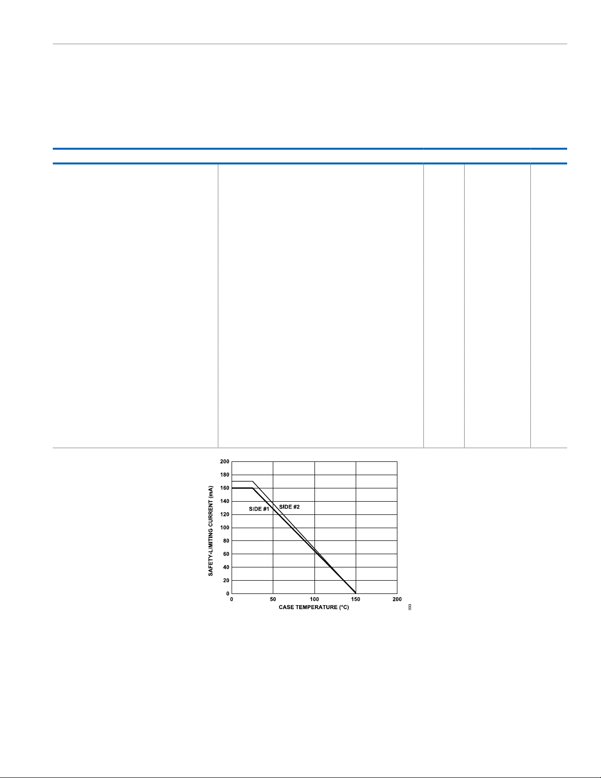
Safety-Limiting Values Maximum value allowed in the event of a failure (see Figure 3)
Case Temperature T
Side 1 Current I
Side 2 Current I
Insulation Resistance at T
S
VIO = 500 V R
S
S1
S2
S
I to IV
I to III
I to II
560 V
396 V
1050 V
4000 V
4000 V
10,000 V
PEAK
RMS
PEAK
PEAK
PEAK
PEAK
PEAK
PEAK
150 °C
160 mA
170 mA
9
>10
Ω
Figure 3. Thermal Derating Curve, Dependence of Safety-Limiting Values on Case Temperature per DIN EN IEC 60747-17 (VDE 0884-17)
analog.com Rev. L | 22 of 31
Page 23

Data Sheet ADuM1200/ADuM1201
SPECIFICATIONS
RECOMMENDED OPERATING CONDITIONS
Table 12.
Parameter Rating
DD1
DD1
, V
, V
DD2
DD2
1
2
1, 3
)
2, 3
)
−40°C to +105°C
−40°C to +125°C
2.7 V to 5.5 V
3.0 V to 5.5 V
Operating Temperature (TA)
Operating Temperature (TA)
Supply Voltages (V
Supply Voltages (V
Input Signal Rise and Fall Times 1.0 ms
1
Does not apply to ADuM1200W and ADuM1201W automotive grade products.
2
Applies to ADuM1200W and ADuM1201W automotive grade products.
3
All voltages are relative to the respective ground. See the DC Correctness and Magnetic Field Immunity section for information on immunity to external magnetic fields.
analog.com Rev. L | 23 of 31
Page 24
Data Sheet ADuM1200/ADuM1201
ABSOLUTE MAXIMUM RATINGS
Ambient temperature = 25°C, unless otherwise noted.
Table 13.
Parameter Rating
Storage Temperature (TST) −55°C to +150°C
Ambient Operating Temperature (TA)
Ambient Operating Temperature (TA)
Supply Voltages (V
Input Voltages (VIA, VIB)
DD1
, V
DD2
3, 4
Output Voltages (VOA, VOB)
Average Output Current per Pin (I
Common-Mode Transients (CML, CMH)
1
Does not apply to ADuM1200W and ADuM1201W automotive grade products.
2
Applies to ADuM1200W and ADuM1201W automotive grade products.
3
All voltages are relative to the respective ground.
4
V
DDI
and V
refer to the supply voltages on the input and output sides of a
DDO
given channel, respectively.
3, 4
1
2
3
)
5
)
O
6
−40°C to +105°C
−40°C to +125°C
−0.5 V to +7.0 V
−0.5 V to V
−0.5 V to V
+ 0.5 V
DDI
+ 0.5 V
DDO
−11 mA to +11 mA
−100 kV/µs to +100 kV/µs
5
See Figure 3 for maximum rated current values for various temperatures.
6
Refers to common-mode transients across the insulation barrier. Commonmode transients exceeding the absolute maximum ratings can cause latch-up
or permanent damage.
Stresses at or above those listed under Absolute Maximum Ratings
may cause permanent damage to the product. This is a stress
rating only; functional operation of the product at these or any other
conditions above those indicated in the operational section of this
specification is not implied. Operation beyond the maximum operating conditions for extended periods may affect product reliability.
ESD CAUTION
ESD (electrostatic discharge) sensitive device. Charged devi-
ces and circuit boards can discharge without detection. Although
this product features patented or proprietary protection circuitry,
damage may occur on devices subjected to high energy ESD.
Therefore, proper ESD precautions should be taken to avoid
performance degradation or loss of functionality.
MAXIMUM CONTINUOUS WORKING VOLTAGE
Table 14. Maximum Continuous Working Voltage
Parameter Max Unit Constraint
AC Voltage
Bipolar Waveform 560 V
1
Refers to continuous voltage magnitude imposed across the isolation barrier. See the Insulation Lifetime section for more details.
1
PEAK
Reinforced insulation rating per IEC 60747-17 (VDE 0884-17)
analog.com Rev. L | 24 of 31
Page 25
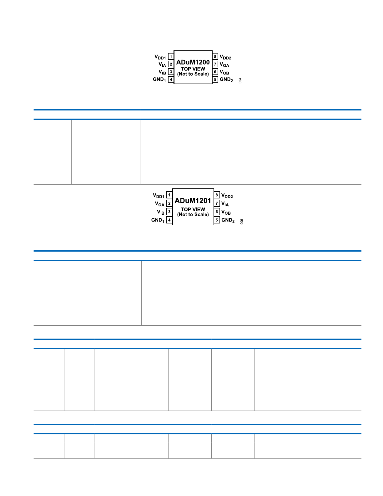
Data Sheet ADuM1200/ADuM1201
PIN CONFIGURATIONS AND FUNCTION DESCRIPTIONS
Figure 4. ADuM1200 Pin Configuration
Table 15. ADuM1200 Pin Function Descriptions
Pin No. Mnemonic Description
1 V
2 V
3 V
DD1
IA
IB
4 GND
5 GND
6 V
7 V
8 V
OB
OA
DD2
1
2
Supply Voltage for Isolator Side 1.
Logic Input A.
Logic Input B.
Ground 1. Ground Reference for Isolator Side 1.
Ground 2. Ground Reference for Isolator Side 2.
Logic Output B.
Logic Output A.
Supply Voltage for Isolator Side 2.
Figure 5. ADuM1201 Pin Configuration
Table 16. ADuM1201 Pin Function Descriptions
Pin No. Mnemonic Description
1 V
2 V
3 V
DD1
OA
IB
4 GND
5 GND
6 V
7 V
8 V
OB
IA
DD2
1
2
Supply Voltage for Isolator Side 1.
Logic Output A.
Logic Input B.
Ground 1. Ground Reference for Isolator Side 1.
Ground 2. Ground Reference for Isolator Side 2.
Logic Output B.
Logic Input A.
Supply Voltage for Isolator Side 2.
Table 17. ADuM1200 Truth Table (Positive Logic)
VIA Input VIB Input V
State V
DD1
State VOA Output VOB Output Notes
DD2
H H Powered Powered H H
L L Powered Powered L L
H L Powered Powered H L
L H Powered Powered L H
X X Unpowered Powered H H Outputs return to the input state within 1 µs of V
DDI
power restoration.
X X Powered Unpowered Indeterminate Indeterminate Outputs return to the input state within 1 µs of V
DDO
power restoration.
Table 18. ADuM1201 Truth Table (Positive Logic)
VIA Input VIB Input V
State V
DD1
State VOA Output VOB Output Notes
DD2
H H Powered Powered H H
L L Powered Powered L L
H L Powered Powered H L
analog.com Rev. L | 25 of 31
Page 26

Data Sheet ADuM1200/ADuM1201
PIN CONFIGURATIONS AND FUNCTION DESCRIPTIONS
Table 18. ADuM1201 Truth Table (Positive Logic) (Continued)
VIA Input VIB Input V
L H Powered Powered L H
X X Unpowered Powered Indeterminate H Outputs return to the input state within 1 µs of V
X X Powered Unpowered H Indeterminate Outputs return to the input state within 1 µs of V
State V
DD1
State VOA Output VOB Output Notes
DD2
power restoration.
DDI
DDO
power restoration.
analog.com Rev. L | 26 of 31
Page 27
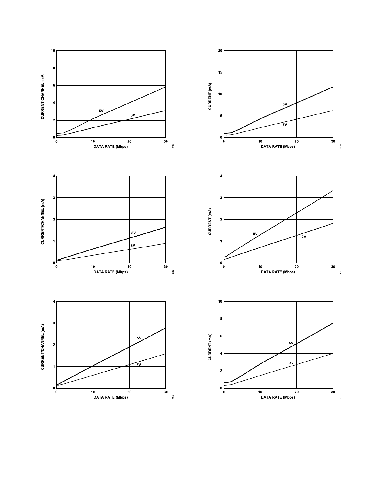
Data Sheet ADuM1200/ADuM1201
TYPICAL PERFORMANCE CHARACTERISTICS
Figure 6. Typical Input Supply Current per Channel vs. Data Rate for 5 V and
3 V Operation
Figure 7. Typical Output Supply Current per Channel vs. Data Rate for 5 V
and 3 V Operation (No Output Load)
Figure 9. Typical ADuM1200 V
Figure 10. Typical ADuM1200 V
Supply Current vs. Data Rate for 5 V and 3
DD1
V Operation
Supply Current vs. Data Rate for 5 V and 3
DD2
V Operation
Figure 8. Typical Output Supply Current per Channel vs. Data Rate for 5 V
and 3 V Operation (15 pF Output Load)
analog.com Rev. L | 27 of 31
Figure 11. Typical ADuM1201 V
V and 3 V Operation
DD1
or V
Supply Current vs. Data Rate for 5
DD2
Page 28
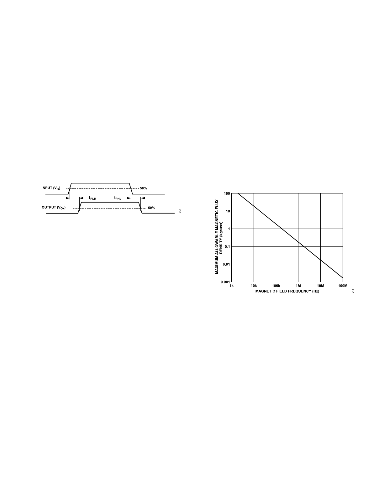
Data Sheet ADuM1200/ADuM1201
APPLICATIONS INFORMATION
PCB LAYOUT
The ADuM1200/ADuM1201 digital isolators require no external
interface circuitry for the logic interfaces. Power supply bypassing is
strongly recommended at the input and output supply pins.
The capacitor value must be between 0.01 µF and 0.1 µF. The total
lead length between both ends of the capacitor and the input power
supply pin must not exceed 20 mm.
See the AN-1109 Application Note for board layout guidelines.
The 3 V operating condition of the ADuM1200/ADuM1201 is examined because it represents the most susceptible mode of operation.
The pulses at the transformer output have an amplitude greater
than 1.0 V. The decoder has a sensing threshold at about 0.5 V,
therefore establishing a 0.5 V margin in which induced voltages can
be tolerated. The voltage induced across the receiving coil is given
by
V = (−dβ/dt)Σ∏r
where:
PROPAGATION DELAY-RELATED PARAMETERS
Propagation delay is a parameter that describes the time it takes
a logic signal to propagate through a component. The propagation
delay to a logic low output can differ from the propagation delay to a
logic high output.
β is the magnetic flux density (gauss).
N is the number of turns in the receiving coil.
rn is the radius of the nth turn in the receiving coil (cm).
Given the geometry of the receiving coil in the ADuM1200/ADuM1201 and an imposed requirement that the induced voltage be
50% at most of the 0.5 V margin at the decoder, a maximum
allowable magnetic field is calculated, as shown in Figure 13.
Figure 12. Propagation Delay Parameters
2
; n = 1, 2, … , N
n
(1)
Pulse width distortion is the maximum difference between these two
propagation delay values and is an indication of how accurately the
timing of the input signal is preserved.
Channel-to-channel matching refers to the maximum amount that
the propagation delay differs between channels within a single
ADuM1200/ADuM1201 component.
Propagation delay skew refers to the maximum amount that the
propagation delay differs between multiple ADuM1200/ADuM1201
components operating under the same conditions.
DC CORRECTNESS AND MAGNETIC FIELD IMMUNITY
Figure 13. Maximum Allowable External Magnetic Flux Density
For example, at a magnetic field frequency of 1 MHz, the maximum
allowable magnetic field of 0.2 kgauss induces a voltage of 0.25 V
at the receiving coil. This is about 50% of the sensing threshold and
Positive and negative logic transitions at the isolator input send
narrow (~1 ns) pulses to the decoder via the transformer. The decoder is bistable and is therefore either set or reset by the pulses,
indicating input logic transitions. In the absence of logic transitions
does not cause a faulty output transition. Similarly, if such an event
occurs during a transmitted pulse (and has the worst-case polarity),
it reduces the received pulse from >1.0 V to 0.75 V—still well above
the 0.5 V sensing threshold of the decoder.
of more than ~1 µs at the input, a periodic set of refresh pulses
indicative of the correct input state is sent to ensure dc correctness
at the output. If the decoder receives no internal pulses for more
than about 5 µs, the input side is assumed to be unpowered or
nonfunctional, in which case the isolator output is forced to a default
state (see Table 17 and Table 18) by the watchdog timer circuit.
The preceding magnetic flux density values correspond to specific current magnitudes at given distances away from the ADuM1200/ADuM1201 transformers. Figure 14 expresses these allowable current magnitudes as a function of frequency for selected
distances. As seen, the ADuM1200/ADuM1201 are extremely immune and can be affected only by extremely large currents oper-
The ADuM1200/ADuM1201 are extremely immune to external magnetic fields. The limitation on the magnetic field immunity of the
ADuM1200/ADuM1201 is set by the condition in which induced
ating very close to the component at a high frequency. For the
1 MHz example, place a 0.5 kA current 5 mm away from the
ADuM1200/ADuM1201 to affect the operation of the component.
voltage in the receiving coil of the transformer is suf-ficiently large
enough to either falsely set or reset the decoder. The following
analysis defines the conditions under which this can occur.
analog.com Rev. L | 28 of 31
Page 29
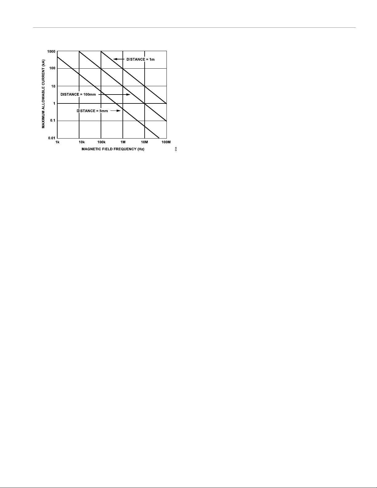
Data Sheet ADuM1200/ADuM1201
APPLICATIONS INFORMATION
where:
I
, I
DDI (D)
per channel (mA/Mbps).
CL is the output load capacitance (pF).
V
is the output supply voltage (V).
DDO
f is the input logic signal frequency (MHz, half of the input data rate,
NRZ signaling).
fr is the input stage refresh rate (Mbps).
I
, I
DDI (Q)
currents (mA).
are the input and output dynamic supply currents
DDO (D)
are the specified input and output quiescent supply
DDO (Q)
To calculate the total I
currents for each input and output channel corresponding to I
and I
DD2
per-channel supply currents as a function of data rate for an
Figure 14. Maximum Allowable Current for Various Current-to-ADuM1200/
ADuM1201 Spacings
unloaded output condition. Figure 8 provides per-channel supply
current as a function of data rate for a 15 pF output condition.
Figure 9 through Figure 11 provide total V
Note that, at combinations of strong magnetic fields and high frequencies, any loops formed by PCB traces can induce sufficiently
current as a function of data rate for ADuM1200 and ADuM1201
channel configurations.
large error voltages to trigger the threshold of succeeding circuitry.
Take care in the layout of such traces to avoid this possibility.
POWER CONSUMPTION
INSULATION LIFETIME
All insulation structures eventually break down when subjected to
voltage stress over a sufficiently long period. The rate of insulation
The supply current at a given channel of the ADuM1200/ADuM1201
isolator is a function of the supply voltage, the data rate of the
channel, and the output load of the channel.
For each input channel, the supply current is given by
degradation is dependent on the characteristics of the voltage
waveform applied across the insulation. In addition to the testing
performed by the regulatory agencies, Analog Devices carries out
an extensive set of evaluations to determine the lifetime of the
insulation structure within the ADuM1200/ADuM1201.
I
DDI
I
DDI
= I
= I
DDI (Q)
DDI (D)
f ≤ 0.5f
r
× (2f − fr) + I
DDI (Q)
f > 0.5f
r
For each output channel, the supply current is given by
I
DDO
I
DDO
> 0.5f
= I
= (I
r
f ≤ 0.5f
DDO (Q)
+ (0.5 × 10⁻³) × CLV
DDO (D)
r
) × (2f − fr) + I
DDO
DDO (Q)
(2)
Analog Devices performs accelerated life testing using voltage
(3)
levels higher than the rated continuous working voltage. Acceleration factors for several operating conditions are determined. These
factors allow calculation of the time to failure at the actual working
(4)
f
(5)
voltage. The values shown in Table 14 summarize the maximum
continuous working voltages as per IEC 60747-17. Operation at
these high working voltages can lead to shortened insulation life in
some cases.
DD1
and I
supply currents, the supply
DD2
DD1
are calculated and totaled. Figure 6 and Figure 7 provide
DD1
and V
supply
DD2
analog.com Rev. L | 29 of 31
Page 30
Data Sheet ADuM1200/ADuM1201
OUTLINE DIMENSIONS
Package Drawing (Option) Package Type Package Description
R-8 SOIC_N 8-Lead Standard Small Outline Package, Narrow Body
For the latest package outline information and land patterns (footprints), go to Package Index.
ORDERING GUIDE
1, 2
Model
ADuM1200AR −40°C to +105°C 8-Lead Narrow-Body SOIC_N Tube, 98 R-8
ADuM1200ARZ −40°C to +105°C 8-Lead Narrow-Body SOIC_N Tube, 98 R-8
ADuM1200ARZ-RL7 −40°C to +105°C 8-Lead Narrow-Body SOIC_N Reel, 1000 R-8
ADuM1200BR −40°C to +105°C 8-Lead Narrow-Body SOIC_N Tube, 98 R-8
ADuM1200BRZ −40°C to +105°C 8-Lead Narrow-Body SOIC_N Tube, 98 R-8
ADuM1200BRZ-RL7 −40°C to +105°C 8-Lead Narrow-Body SOIC_N Reel, 1000 R-8
ADuM1200CR −40°C to +105°C 8-Lead Narrow-Body SOIC_N Tube, 98 R-8
ADuM1200CRZ −40°C to +105°C 8-Lead Narrow-Body SOIC_N Tube, 98 R-8
ADuM1200CRZ-RL7 −40°C to +105°C 8-Lead Narrow-Body SOIC_N Reel, 1000 R-8
ADuM1200WSRZ −40°C to +125°C 8-Lead Narrow-Body SOIC_N Tube, 98 R-8
ADuM1200WSRZ-RL7 −40°C to +125°C 8-Lead Narrow-Body SOIC_N Reel, 1000 R-8
ADuM1200WTRZ −40°C to +125°C 8-Lead Narrow-Body SOIC_N Tube, 98 R-8
ADuM1200WTRZ-RL7 −40°C to +125°C 8-Lead Narrow-Body SOIC_N Reel, 1000 R-8
ADuM1200WURZ −40°C to +125°C 8-Lead Narrow-Body SOIC_N Tube, 98 R-8
ADuM1200WURZ-RL7 −40°C to +125°C 8-Lead Narrow-Body SOIC_N Reel, 1000 R-8
ADuM1201AR −40°C to +105°C 8-Lead Narrow-Body SOIC_N Tube, 98 R-8
ADuM1201AR-RL7 −40°C to +105°C 8-Lead Narrow-Body SOIC_N Reel, 1000 R-8
ADuM1201ARZ −40°C to +105°C 8-Lead Narrow-Body SOIC_N Tube, 98 R-8
ADuM1201ARZ-RL7 −40°C to +105°C 8-Lead Narrow-Body SOIC_N Reel, 1000 R-8
ADuM1201BR −40°C to +105°C 8-Lead Narrow-Body SOIC_N Tube, 98 R-8
ADuM1201BR-RL7 −40°C to +105°C 8-Lead Narrow-Body SOIC_N Reel, 1000 R-8
ADuM1201BRZ −40°C to +105°C 8-Lead Narrow-Body SOIC_N Tube, 98 R-8
ADuM1201BRZ-RL7 −40°C to +105°C 8-Lead Narrow-Body SOIC_N Reel, 1000 R-8
ADuM1201CR −40°C to +105°C 8-Lead Narrow-Body SOIC_N Tube, 98 R-8
ADuM1201CRZ −40°C to +105°C 8-Lead Narrow-Body SOIC_N Tube, 98 R-8
ADuM1201CRZ-RL7 −40°C to +105°C 8-Lead Narrow-Body SOIC_N Reel, 1000 R-8
ADuM1201WSRZ −40°C to +125°C 8-Lead Narrow-Body SOIC_N Tube, 98 R-8
ADuM1201WSRZ-RL7 −40°C to +125°C 8-Lead Narrow-Body SOIC_N Reel, 1000 R-8
ADuM1201WTRZ −40°C to +125°C 8-Lead Narrow-Body SOIC_N Tube, 98 R-8
ADuM1201WTRZ-RL7 −40°C to +125°C 8-Lead Narrow-Body SOIC_N Reel, 1000 R-8
ADuM1201WURZ −40°C to +125°C 8-Lead Narrow-Body SOIC_N Tube, 98 R-8
ADuM1201WURZ-RL7 −40°C to +125°C 8-Lead Narrow-Body SOIC_N Reel, 1000 R-8
Temperature Range Package Description Packing Quantity Package Option
1
Z = RoHS Compliant Part.
2
W = Qualified for Automotive Applications.
analog.com Rev. L | 30 of 31
Page 31
Data Sheet ADuM1200/ADuM1201
OUTLINE DIMENSIONS
NUMBER OF INPUTS, MAXIMUM DATA RATE, MAXIMUM PROPAGATION DELAY, AND MAXIMUM PULSE WIDTH DISTORTION OPTIONS
1, 2
Model
ADuM1200AR 2 0 1 150 40
ADuM1200ARZ 2 0 1 150 40
ADuM1200ARZ-RL7 2 0 1 150 40
ADuM1200BR 2 0 10 50 3
ADuM1200BRZ 2 0 10 50 3
ADuM1200BRZ-RL7 2 0 10 50 3
ADuM1200CR 2 0 25 45 3
ADuM1200CRZ 2 0 25 45 3
ADuM1200CRZ-RL7 2 0 25 45 3
ADuM1200WSRZ 2 0 1 150 40
ADuM1200WSRZ-RL7 2 0 1 150 40
ADuM1200WTRZ 2 0 10 50 3
ADuM1200WTRZ-RL7 2 0 10 50 3
ADuM1200WURZ 2 0 25 45 3
ADuM1200WURZ-RL7 2 0 25 45 3
ADuM1201AR 1 1 1 150 40
ADuM1201AR-RL7 1 1 1 150 40
ADuM1201ARZ 1 1 1 150 40
ADuM1201ARZ-RL7 1 1 1 150 40
ADuM1201BR 1 1 10 50 3
ADuM1201BR-RL7 1 1 10 50 3
ADuM1201BRZ 1 1 10 50 3
ADuM1201BRZ-RL7 1 1 10 50 3
ADuM1201CR 1 1 25 45 3
ADuM1201CRZ 1 1 25 45 3
ADuM1201CRZ-RL7 1 1 25 45 3
ADuM1201WSRZ 1 1 1 150 40
ADuM1201WSRZ-RL7 1 1 1 150 40
ADuM1201WTRZ 1 1 10 50 3
ADuM1201WTRZ-RL7 1 1 10 50 3
ADuM1201WURZ 1 1 25 45 3
ADuM1201WURZ-RL7 1 1 25 45 3
Number of Inputs, V
Side
Number of Inputs, V
DD1
Side
Maximum Data Rate
DD2
(Mbps)
Maximum Propagation
Delay, 5 V (ns)
Maximum Pulse Width
Distortion (ns)
1
Z = RoHS Compliant Part.
2
W = Qualified for Automotive Applications.
AUTOMOTIVE PRODUCTS
The ADuM1200W and ADuM1201W models are available with controlled manufacturing to support the quality and reliability requirements
of automotive applications. Note that these automotive models may have specifications that differ from the commercial models; therefore,
designers should review the Specifications section of this data sheet carefully. Only the automotive grade products shown are available for use
in automotive applications. Contact your local Analog Devices account representative for specific product ordering information and to obtain the
specific Automotive Reliability reports for these models.
©2004-2025 Analog Devices, Inc. All rights reserved. Trademarks and
registered trademarks are the property of their respective owners.
One Analog Way, Wilmington, MA 01887-2356, U.S.A.
Rev. L | 31 of 31
 Loading...