

Page 1
Data Sheet
ADP2138/ADP2139
Compact, 800 mA, 3 MHz, Step-Down DC-to-DC Converter
FEATURES
► Input voltage: 2.3 V to 5.5 V
► Peak efficiency: 95%
► 3 MHz fixed frequency operation
► Typical quiescent current: 23 μA
► Very small solution size
► 6-lead, 1 mm × 1.5 mm WLCSP package
► Fast load and line transient response
► 100% duty cycle low dropout mode
► Internal synchronous rectifier, compensation, and soft start
► Current overload and thermal shutdown protections
► Ultralow shutdown current: 0.2 μA (typical)
► Forced PWM and automatic PWM/PSM modes
► Supported by ADIsimPower
™
design tool
APPLICATIONS
► PDAs and palmtop computers
► Wireless handsets
► Digital audio, portable media players
► Digital cameras, GPS navigation units
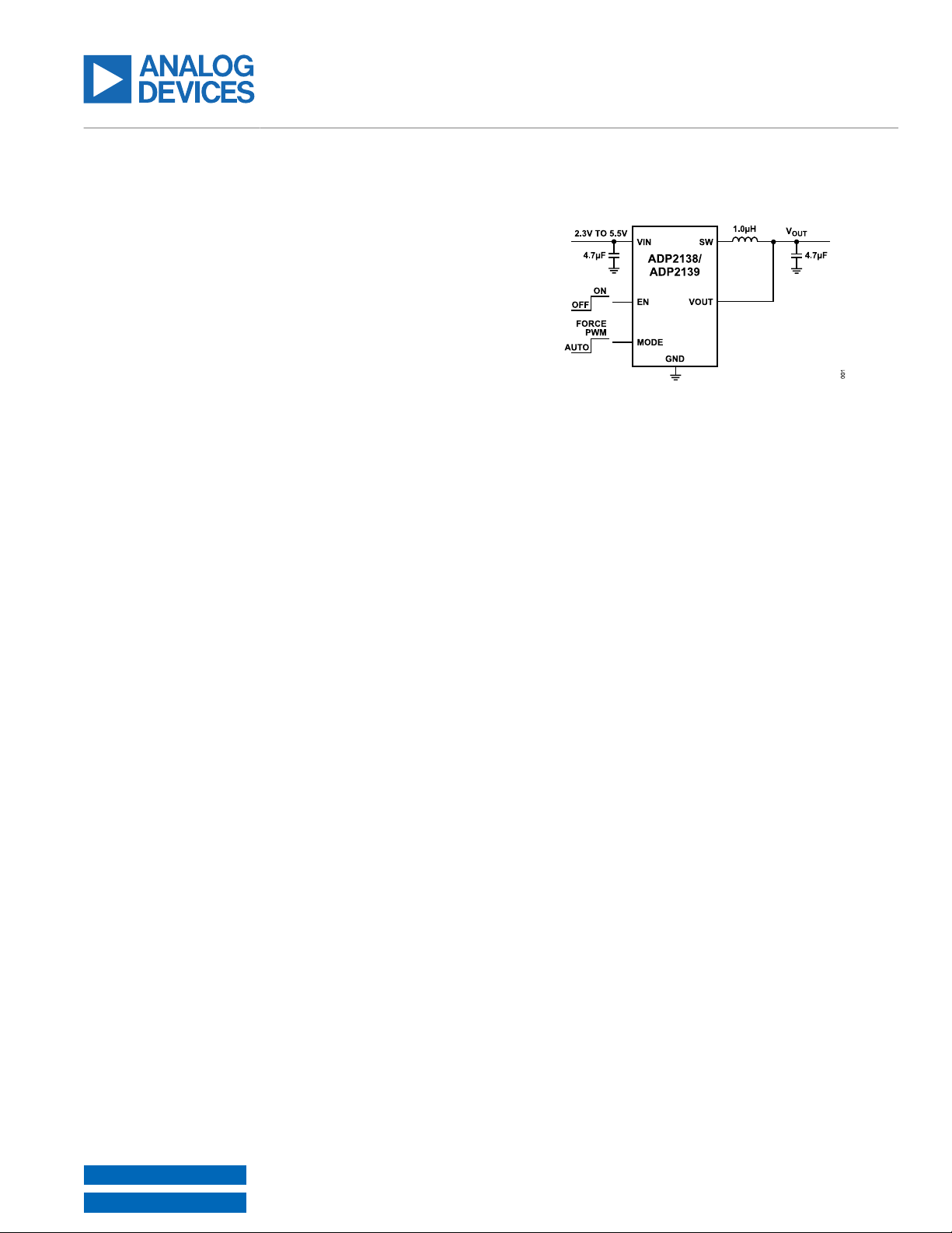
TYPICAL APPLICATIONS CIRCUIT
Figure 1.
GENERAL DESCRIPTION
The ADP2138 and ADP2139 are high efficiency, low quiescent
current, synchronous step-down dc-to-dc converters. The ADP2139
has the additional feature of an internal discharge switch. The total
solution requires only three tiny external components. When the
MODE pin is set high, the buck regulator operates in forced PWM
mode, which provides low peak-to-peak ripple for power supply
noise sensitive loads at the expense of light load efficiency. When
the MODE pin is set low, the buck regulator automatically switches
operating modes, depending on the load current level. At higher
output loads, the buck regulator operates in PWM mode. When
the load current falls below a predefined threshold, the regulator
operates in power save mode (PSM), improving light load efficiency.
The ADP2138/ADP2139 operate on input voltages of 2.3 V to 5.5
V, which allows for single lithium or lithium polymer cell, multiple
alkaline or NiMH cell, PCMCIA, USB, and other standard power
sources. The maximum load current of 800 mA is achievable
across the input voltage range.
The ADP2138/ADP2139 are available in fixed output voltages of
3.3 V, 3.0 V, 2.8 V, 2.5 V, 1.8 V, 1.5 V, 1.2 V, 1.0 V, and 0.8
V. All versions include an internal power switch and synchronous
rectifier for minimal external part count and high efficiency. The
ADP2138/ADP2139 have internal soft start and they are internally
compensated. During logic controlled shutdown, the input is disconnected from the output and the ADP2138/ADP2139 draw 0.2 μA
(typical) from the input source.
Other key features include undervoltage lockout to prevent deep
battery discharge, and soft start to prevent input current over-shoot
at startup. The ADP2138/ADP2139 are available in a 6-ball wafer
level chip scale package (WLCSP).
Rev. E
DOCUMENT FEEDBACK
TECHNICAL SUPPORT
Information furnished by Analog Devices is believed to be accurate and reliable "as is". However, no responsibility is assumed by Analog Devices
for its use, nor for any infringements of patents or other rights of third parties that may result from its use. Specifications subject to change
without notice. No license is granted by implication or otherwise under any patent or patent rights of Analog Devices. Trademarks and registered
trademarks are the property of their respective owners. All Analog Devices products contained herein are subject to release and availability.
Page 2

Data Sheet ADP2138/ADP2139
TABLE OF CONTENTS
Features................................................................ 1
Applications........................................................... 1
Typical Applications Circuit....................................1
General Description...............................................1
Specifications........................................................ 3
Input and Output Capacitor, Recommended
Specifications................................................... 3
Absolute Maximum Ratings...................................4
Thermal Data......................................................4
Thermal Resistance........................................... 4
ESD Caution.......................................................4
Pin Configuration and Function Descriptions........ 5
Typical Performance Characteristics.....................6
Theory of Operation.............................................11
Control Scheme................................................11
PWM Mode.......................................................11
Power Save Mode............................................ 11
Enable/Shutdown............................................. 12
REVISION HISTORY
4/2025—Rev. D to Rev. E
Change to Features Section............................................................................................................................ 1
Added Output Voltage Option .......................................................................................................................18
Short-Circuit Protection.................................... 12
Undervoltage Lockout...................................... 12
Thermal Protection...........................................12
Soft Start.......................................................... 12
Current Limit.....................................................12
100% Duty Operation.......................................12
Discharge Switch..............................................12
Applications Information...................................... 14
ADIsimPower Design Tool................................14
External Component Selection.........................14
Thermal Considerations................................... 15
PCB Layout Guidelines.................................... 15
Evaluation Board................................................. 17
Evaluation Board Layout.................................. 17
Outline Dimensions............................................. 18
Ordering Guide.................................................18
Output Voltage Option......................................18
Evaluation Boards............................................ 19
analog.com Rev. E | 2 of 19
Page 3
Data Sheet ADP2138/ADP2139
SPECIFICATIONS
VIN = 3.6 V, V
= 0.8 V − 3.3 V, TJ = −40°C to +125°C for minimum/maximum specifications, and T
OUT
= 25°C for typical specifications, unless
A
otherwise noted. All limits at temperature extremes are guaranteed via correlation using standard statistical quality control (SQC).
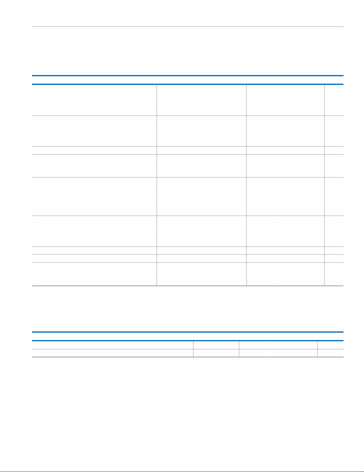
Table 1.
Parameter Test Conditions/Comments Min Typ Max Unit
INPUT CHARACTERISTICS
Input Voltage Range 2.3 5.5 V
Undervoltage Lockout Threshold VIN rising 2.3 V
VIN falling 2.00 2.15 2.25 V
OUTPUT CHARACTERISTICS
Output Voltage Accuracy PWM mode −2 +2 %
Line Regulation VIN = 2.3 V to 5.5 V, PWM mode 0.25 %/V
Load Regulation I
PWM TO POWER SAVE MODE CURRENT THRESHOLD 100 mA
INPUT CURRENT CHARACTERISTICS
DC Operating Current I
Shutdown Current EN = 0 V, TA = TJ = −40°C to +85°C 0.2 1.0 μA
SW CHARACTERISTICS
SW On Resistance PFET 155 240 mΩ
Current Limit PFET switch peak current limit 1100 1500 1650 mA
Discharge Switch (ADP2139) 100 Ω
ENABLE AND MODE CHARACTERISTICS
Input High Threshold 1.2 V
Input Low Threshold 0.4 V
Input Leakage Current EN/MODE = 0 V (min), 3.6 V (max ) −1 0 +1 μA
OSCILLATOR FREQUENCY 2.6 3.0 3.4 MHz
START-UP TIME 250 μs
THERMAL CHARACTERISTICS
Thermal Shutdown Threshold 150 °C
Thermal Shutdown Hysteresis 20 °C
= 0 mA − 800 mA −0.95 %/A
LOAD
= 0 mA, device not switching 23 30 μA
LOAD
NFET 115 200 mΩ
INPUT AND OUTPUT CAPACITOR, RECOMMENDED SPECIFICATIONS
TA = −40°C to +125°C, unless otherwise specified. All limits at temperature extremes are guaranteed via correlation using standard statistical
quality control (SQC).
Table 2.
Parameter Symbol Min Typ Max Unit
MINIMUM INPUT AND OUTPUT CAPACITANCE C
CAPACITOR ESR R
analog.com Rev. E | 3 of 19
MIN
ESR
4.7 µF
0.001 1 Ω
Page 4
Data Sheet ADP2138/ADP2139
ABSOLUTE MAXIMUM RATINGS
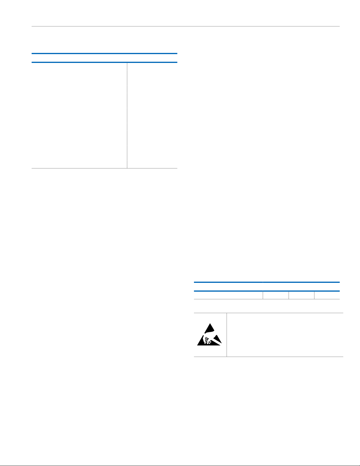
Table 3.
Parameter Rating
VIN, EN, MODE −0.4 V to +6.5 V
VOUT, SW to GND −1.0 V to (VIN + 0.2 V)
Temperature Range
Operating Ambient −40°C to +85°C
Operating Junction −40°C to +125°C
Storage Temperature −65°C to +150°C
Lead Temperature Range −65°C to +150°C
Soldering (10 sec) 300°C
Vapor Phase (60 sec) 215°C
Infrared (15 sec) 220°C
ESD Model
Human Body ±1500 V
Charged Device ±500 V
Machine ±100 V
Stresses at or above those listed under Absolute Maximum Ratings
may cause permanent damage to the product. This is a stress
rating only; functional operation of the product at these or any other
conditions above those indicated in the operational section of this
specification is not implied. Operation beyond the maximum operating conditions for extended periods may affect product reliability.
THERMAL DATA
Absolute maximum ratings apply individually only, not in combination.
ADP2138/ADP2139 can be damaged when the junction temperature limits are exceeded. Monitoring ambient temperature does not
guarantee that the junction temperature (T
) is within the specified
J
Junction-to-ambient thermal resistance (θJA) of the package is
based on modeling and calculation using a 4-layer board. The
junction-to-ambient thermal resistance is highly dependent on the
application and board layout. In applications where high maximum
power dissipation exists, close attention to thermal board design is
required. The value of θJA may vary, depending on PCB material,
layout, and environmental conditions. The specified values of θ
are based on a 4-layer, 4 in. × 3 in., circuit board. Refer to JEDEC
JESD 51-9 for detailed information pertaining to board construction.
For additional information, see the AN-617 Application Note.
ΨJB is the junction-to-board thermal characterization parameter
measured in units of °C/W. ΨJB of the package is based on
modeling and calculation using a 4-layer board. The JESD51-12,
Guidelines for Reporting and Using Package Thermal Information,
states that thermal characterization parameters are not the same as
thermal resistances. ΨJB measures the component power flowing
through multiple thermal paths rather than through a single path,
which is the procedure for measuring thermal resistance, θJB.
Therefore, ΨJB thermal paths include convection from the top of
the package as well as radiation from the package; factors that
make ΨJB more useful in real-world applications than θJB. Maximum
junction temperature (T
(TB) and power dissipation (P
TJ = TB + (PD × ΨJB)
Refer to JEDEC JESD51-8 and JESD51-12 for more detailed
information about ΨJB.
THERMAL RESISTANCE
θJA and ΨJB are specified for the worst-case conditions, that is, a
device soldered in a circuit board for surface-mount packages.
temperature limits. In applications with high power dissipation and
poor thermal resistance, the maximum ambient temperature may
need to be derated. In applications with moderate power dissipation
and low printed circuit board (PCB) thermal resistance, the maxi-
Table 4. Thermal Resistance
Package Type θ
6-Ball WLCSP 170 80 °C/W
mum ambient temperature can exceed the maximum limit for as
long as the junction temperature is within specification limits. The
junction temperature (T
temperature (TA), the power dissipation of the device (P
) of the device is dependent on the ambient
J
), and
D
ESD CAUTION
the junction-to-ambient thermal resistance of the package (θJA).
Maximum junction temperature (T
temperature (TA) and power dissipation (P
TJ = TA + (PD × θJA)
) is calculated from the ambient
J
) using the formula
D
(1)
JA
) is calculated from the board temperature
J
) using the formula
D
(2)
JA
ESD (electrostatic discharge) sensitive device. Charged devi-
ces and circuit boards can discharge without detection. Although
this product features patented or proprietary protection circuitry,
damage may occur on devices subjected to high energy ESD.
Therefore, proper ESD precautions should be taken to avoid
performance degradation or loss of functionality.
Ψ
JB
Unit
analog.com Rev. E | 4 of 19
Page 5
Data Sheet ADP2138/ADP2139
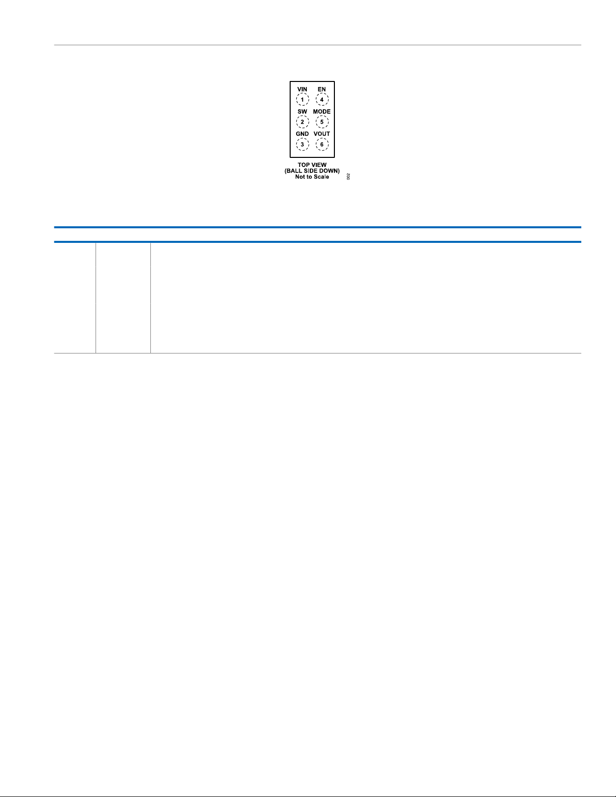
PIN CONFIGURATION AND FUNCTION DESCRIPTIONS
Figure 2. Pin Configuration (Top View)
Table 5. Pin Function Descriptions
Pin No. Mnemonic Description
1 VIN Power Source Input. VIN is the source of the PFET high-side switch. Bypass VIN to GND with a 4.7 µF or greater capacitor as close to the
ADP2138/ADP2139 as possible.
2 SW Switch Node Output. SW is the drain of the P-channel MOSFET switch and N-channel synchronous rectifier. Connect the output LC filter
between SW and the output voltage.
3 GND Ground. Connect the input and output capacitors to GND.
4 EN Buck Activation. To turn on the buck, set EN to high. To turn off the buck, set EN to low.
5 MODE Mode Input. Drive the MODE pin high for the operating mode to force continuous PWM switching. Drive the MODE pin low to allow automatic
PWM/PSM operating mode.
6 VOUT Output Voltage Sensing Input.
analog.com Rev. E | 5 of 19
Page 6
Data Sheet ADP2138/ADP2139
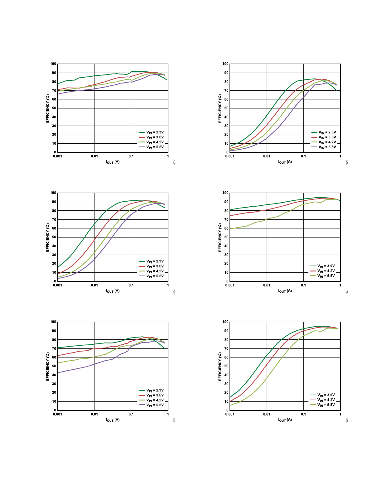
TYPICAL PERFORMANCE CHARACTERISTICS
VIN = 3.6 V, TA = 25°C, VEN = VIN, unless otherwise noted.
Figure 3. Efficiency vs. Load Current, Across Input Voltage, V
OUT
PSM Mode
Figure 4. Efficiency vs. Load Current, Across Input Voltage,V
OUT
PWM Mode
= 1.8 V,
= 1.8 V,
Figure 6. Efficiency vs. Load Current, Across Input Voltage, V
OUT
PWM Mode
Figure 7. Efficiency vs. Load Current, Across Input Voltage, V
OUT
PSM Mode
= 0.8 V,
= 3.3 V,
Figure 5. Efficiency vs. Load Current, Across Input Voltage, V
PSM Mode
OUT
= 0.8 V,
Figure 8. Efficiency vs. Load Current, Across Input Voltage, V
OUT
PWM Mode
= 3.3 V,
analog.com Rev. E | 6 of 19
Page 7
Data Sheet ADP2138/ADP2139
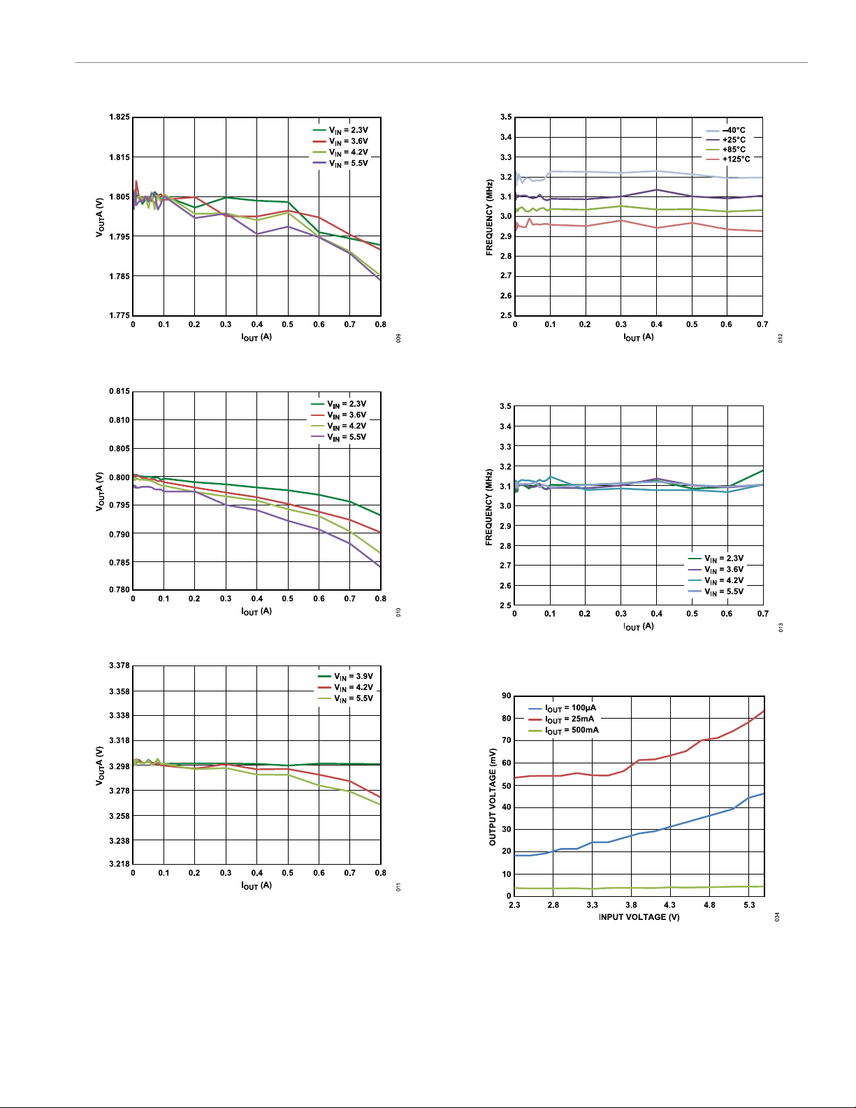
TYPICAL PERFORMANCE CHARACTERISTICS
Figure 9. Load Regulation Across Input Voltage, V
Figure 10. Load Regulation Across Input Voltage, V
OUT
OUT
= 1.8 V, PWM Mode
= 0.8 V, PWM Mode
Figure 12. Frequency vs. Output Current, Across Temperature, V
OUT
PWM Mode
Figure 13. Frequency vs. Output Current, Across Supply Voltage, V
OUT
V
= 1.8 V,
= 1.8
Figure 11. Load Regulation Across Input Voltage, V
= 3.3 V, PWM Mode
OUT
Figure 14. Output Voltage Ripple vs. Input Voltage, Across Output Current,
V
= 1.8 V
OUT
analog.com Rev. E | 7 of 19
Page 8
Data Sheet ADP2138/ADP2139
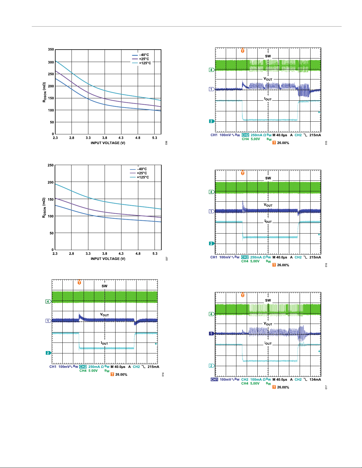
TYPICAL PERFORMANCE CHARACTERISTICS
Figure 15. R
Figure 16. R
DSON
DSON
PFET vs. Input Voltage, Across Temperature
NFET vs. Input Voltage, Across Temperature
Figure 18. Response to Load Transient, 50 mA to 500 mA, V
OUT
= 1.8 V,
Automatic Mode
Figure 19. Response to Load Transient, 150 mA to 500 mA, V
OUT
= 0.8 V,
PWM Mode
Figure 17. Response to Load Transient, 150 mA to 500 mA,V
= 1.8 V, PWM
OUT
Mode
Figure 20. Response to Load Transient, 50 mA to 200 mA, V
OUT
= 0.8 V,
Automatic Mode
analog.com Rev. E | 8 of 19
Page 9
Data Sheet ADP2138/ADP2139
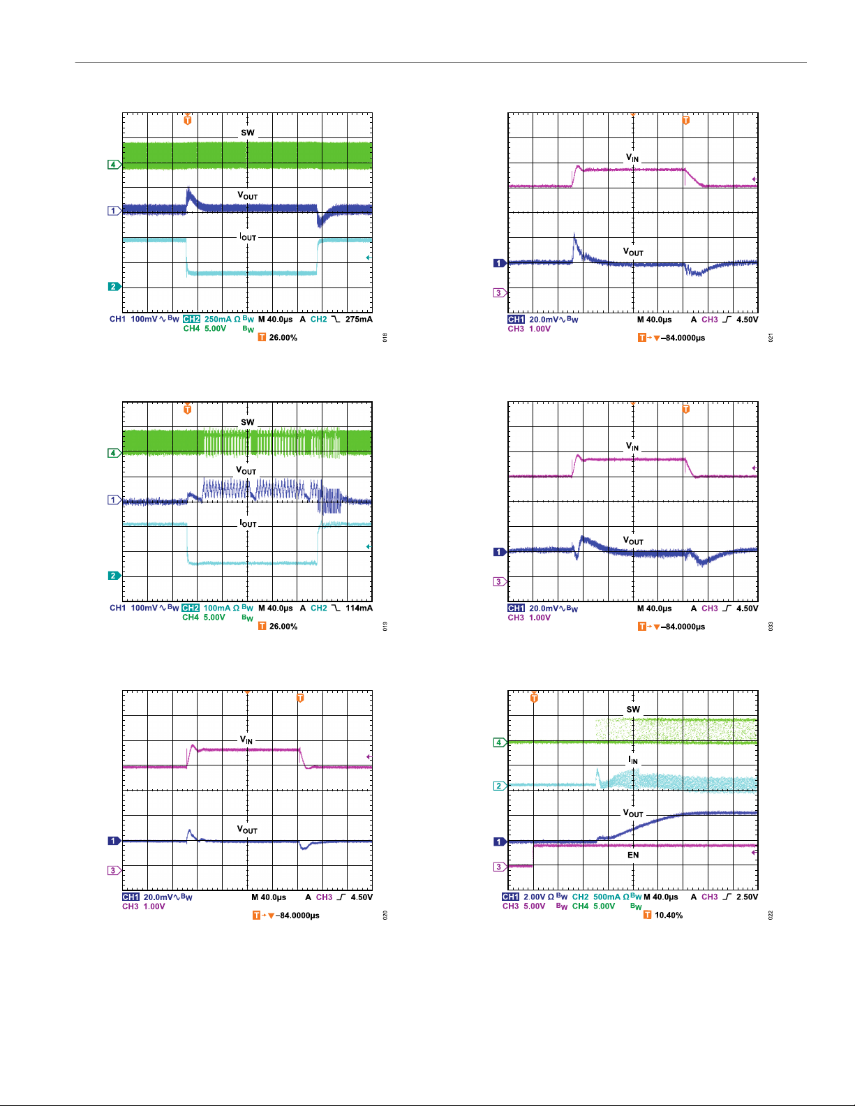
TYPICAL PERFORMANCE CHARACTERISTICS
Figure 21. Response to Load Transient, 150 mA to 500 mA, V
OUT
= 3.3 V,
PWM Mode
Figure 22. Response to Load Transient, 50 mA to 200 mA,V
OUT
= 3.3 V,
Automatic Mode
Figure 24. Response to Line Transient, V
OUT
Mode
Figure 25. Response to Line Transient, V
OUT
Mode
= 0.8 V, VIN = 4.0 V to 4.8 V, PWM
= 1.8 V, VIN = 4.0 V to 4.8 V, PWM
Figure 23. Response to Line Transient, V
= 3.3 V, VIN = 4.0 V to 4.8 V, PWM
OUT
Figure 26. Startup, V
= 1.8 V, I
OUT
= 10 mA
OUT
Mode
analog.com Rev. E | 9 of 19
Page 10
Data Sheet ADP2138/ADP2139
TYPICAL PERFORMANCE CHARACTERISTICS
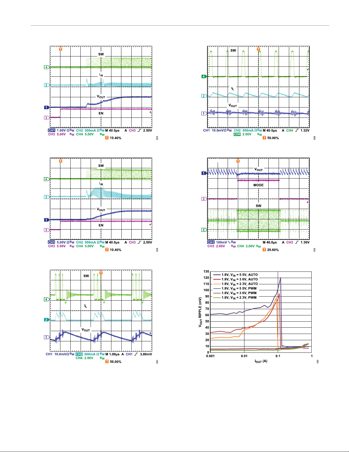
Figure 27. Startup, V
Figure 28. Startup, V
= 0.8 V, I
OUT
= 3.3 V, I
OUT
= 10 mA
OUT
= 10 mA
OUT
Figure 30. Typical Waveform, V
Figure 31. Mode Transition from PSM to PWM to PSM, V
= 1.8 V, PWM Mode, I
OUT
= 200 mA
OUT
= 1.8 V
OUT
Figure 29. Typical Waveform, V
= 1.8 V, PSM Mode, I
OUT
= 10 mA
OUT
Figure 32. V
OUT
Peak-to-Peak Ripple vs. Output Current, V
= 1.8 V
OUT
analog.com Rev. E | 10 of 19
Page 11
Data Sheet ADP2138/ADP2139
THEORY OF OPERATION
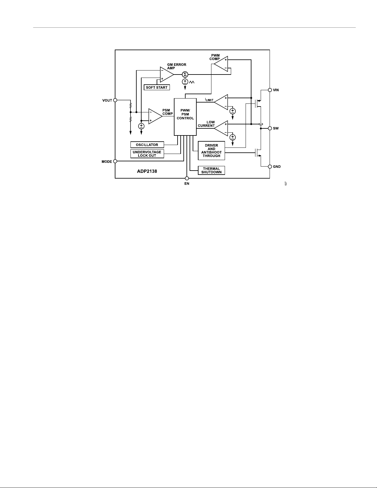
Figure 33. ADP2138 Functional Block Diagram
The ADP2138 and ADP2139 are step-down dc-to-dc converters
that use a fixed frequency and high speed current-mode architecture. The high switching frequency and tiny 6-ball WLCSP package
allow for a small step-down dc-to-dc converter solution.
The ADP2138/ADP2139 operate with an input voltage of 2.3 V to
5.5 V, and regulate an output voltage down to 0.8 V.
CONTROL SCHEME
The ADP2138/ADP2139 operate with a fixed frequency, currentmode PWM control architecture at medium to high loads for high
efficiency, but shift to a power save mode control scheme at light
loads to lower the regulation power losses. When operating in PWM
mode, the duty cycle of the integrated switches is adjusted and regulates the output voltage. When operating in power save mode at
light loads, the output voltage is controlled in a hysteretic manner,
with higher V
ripple. During part of this time, the converter is
OUT
able to stop switching and enters an idle mode, which improves
conversion efficiency. Each ADP2138/ADP2139 has a MODE pin,
which determines the operation of the buck regulator in either PWM
mode (when the MODE pin is set high) or power save mode (when
the mode pin is set low).
PWM MODE
In PWM mode, the ADP2138/ADP2139 operate at a fixed frequency of 3 MHz, set by an internal oscillator. At the start of each oscilla-
The ADP2138/ADP2139 regulate the output voltage by adjusting
the peak inductor current threshold.
POWER SAVE MODE
The ADP2138/ADP2139 smoothly transition to the power save
mode of operation when the load current decreases below the power save mode current threshold. When the ADP2138 and ADP2139
enter power save mode, an offset is induced in the PWM regulation
level, which makes the output voltage rise. When the output voltage
reaches a level approximately 1.5% above the PWM regulation
level, PWM operation turns off. At this point, both power switches
are off, and the ADP2138/ADP2139 enter into idle mode. C
discharges until V
point the device drives the inductor to cause V
the upper threshold. This process is repeated for as long as the
load current is below the power save mode current threshold.
Power Save Mode Current Threshold
The power save mode current threshold is set to 100 mA. The
ADP2138/ADP2139 employ a scheme that enables this current to
remain accurately controlled, independent of V
This scheme also ensures that there is very little hysteresis between the power save mode current threshold for entry to and exit
from the power save mode. The power save mode current threshold is optimized for excellent efficiency across all load currents.
tor cycle, the PFET switch is turned on, sending a positive voltage
across the inductor. Current in the inductor increases until the
current sense signal crosses the peak inductor current threshold
that turns off the PFET switch and turns on the NFET synchronous
rectifier. This sends a negative voltage across the inductor, causing
the inductor current to decrease. The synchronous rectifier stays on
for the rest of the cycle.
OUT
OUT
levels.
falls to the PWM regulation voltage, at which
OUT
to rise again to
OUT
and V
IN
analog.com Rev. E | 11 of 19
Page 12

Data Sheet ADP2138/ADP2139
THEORY OF OPERATION
ENABLE/SHUTDOWN
The ADP2138/ADP2139 start operating with soft start when the
EN pin is toggled from logic low to logic high. Pulling the EN pin
low forces the device into shutdown mode, reducing the shutdown
current to 0.2 μA (typical).
thereby limiting the inrush current. This prevents possible input
voltage drops when a battery or a high impedance power source is
connected to the input of the converter.
After the EN pin is driven high, internal circuits begin to power up.
Start-up time in the ADP2138/ADP2139 is the measure of when the
output is in regulation after the EN pin is driven high. Start-up time
SHORT-CIRCUIT PROTECTION
The ADP2138/ADP2139 include frequency fold back to prevent
consists of the power-up time and the soft start time.
CURRENT LIMIT
output current runaway on a hard short. When the voltage at the
feedback pin falls below half the target output voltage, indicating
the possibility of a hard short at the output, the switching frequency
is reduced to half the internal oscillator frequency. The reduction
in the switching frequency allows more time for the inductor to
discharge, preventing a runaway of output current.
Each ADP2138/ADP2139 has protection circuitry to limit the
amount of positive current flowing through the PFET switch and
the synchronous rectifier. The positive current limit on the power
switch limits the amount of current that can flow from the input to
the output. The negative current limit prevents the inductor current
from reversing direction and flowing out of the load.
UNDERVOLTAGE LOCKOUT
100% DUTY OPERATION
To protect against battery discharge, undervoltage lockout (UVLO)
circuitry is integrated on the ADP2138/ADP2139. If the input
voltage drops below the 2.15 V UVLO threshold, the ADP2138/
ADP2139 shut down, and both the power switch and the synchronous rectifier turn off. When the voltage rises above the UVLO
threshold, the soft start period is initiated, and the part is enabled.
With a drop in VIN or with an increase in I
ADP2139 reach a limit where, even with the PFET switch on
100% of the time, V
At this limit, the ADP2138/ADP2139 smoothly transition to a mode
where the PFET switch stays on 100% of the time. When the
input conditions change again and the required duty cycle falls, the
THERMAL PROTECTION
In the event that the ADP2138/ADP2139 junction temperature rises
above 150°C, the thermal shutdown circuit turns off the converter.
ADP2138/ADP2139 immediately restart PWM regulation without
allowing overshoot on V
DISCHARGE SWITCH
Extreme junction temperatures can be the result of high current
operation, poor circuit board design, or high ambient temperature. A
20°C hysteresis is included so that when thermal shutdown occurs,
the ADP2138/ADP2139 do not return to operation until the on-chip
temperature drops below 130°C. When coming out of thermal
The ADP2139 has an integrated switched resistor (of typically 100
Ω) to discharge the output capacitor when the EN pin goes low or
when the device enters undervoltage lockout or thermal shutdown.
The time to discharge is typically 200 μs.
shutdown, soft start is initiated.
, the ADP2138/
LOAD
drops below the desired output voltage.
OUT
.
OUT
SOFT START
The ADP2138/ADP2139 have an internal soft start function that
ramps the output voltage in a controlled manner upon startup,
analog.com Rev. E | 12 of 19
Page 13
Data Sheet ADP2138/ADP2139
THEORY OF OPERATION
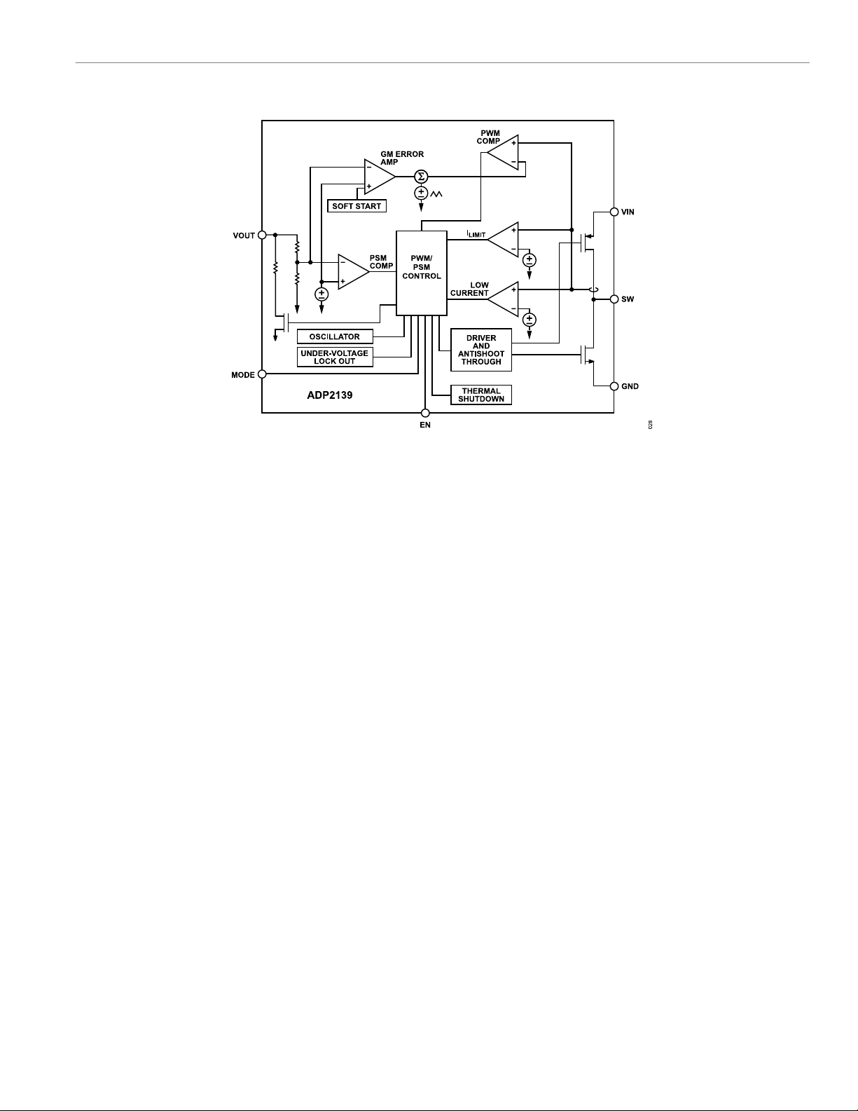
Figure 34. ADP2139 Functional Block Diagram
analog.com Rev. E | 13 of 19
Page 14

Data Sheet ADP2138/ADP2139
APPLICATIONS INFORMATION
ADISIMPOWER DESIGN TOOL
The ADP2138/ADP2139 is supported by ADIsimPower design tool
set. ADIsimPower is a collection of tools that produce complete
power designs optimized for a specific design goal. The tools
Table 6. Suggested 1.0 μH Inductors
Vendor Model
Murata LQM2MPN1R0NG0B 2.0 × 1.6 × 0.9 1400 85
enable the user to generate a full schematic, bill of materials,
and calculate performance in minutes. ADIsimPower can optimize
Taiyo Yuden CBMF1608T1R0M 1.6 × 0.8 × 0.8 290 90
designs for cost, area, efficiency, and parts count while taking into
consideration the operating conditions and limitations of the IC and
Coilcraft TDK GLFR1608T1R0M-LR 1.6 × 0.8 × 0.8 360 80
all real external components. For more information about ADIsimPower design tools, refer to https://www.analog.com/ADIsimPower.
Coilcraft Toko MDT2520-CN 2.5 × 2.0 × 1.2 1800 100
The tool set is available from this website, and users can also
request an unpopulated board through the tool.
EXTERNAL COMPONENT SELECTION
Trade-offs between performance parameters such as efficiency and
transient response can be made by varying the choice of external
components in the applications circuit, as shown in Figure 1.
Output Capacitor
Higher output capacitor values reduce the output voltage ripple and
improve load transient response. When choosing this value, it is
also important to account for the loss of capacitance due to output
voltage dc bias.
Ceramic capacitors are manufactured with a variety of dielectrics,
Inductor
The high switching frequency of the ADP2138/ADP2139 allows
for the selection of small chip inductors. For best performance,
use inductor values between 0.7 μH and 3 μH. Recommended
inductors are shown in Table 6.
The peak-to-peak inductor current ripple is calculated using the
following equation:
V
× VIN− V
I
RIPPLE
=
OUT
VIN× fSW× L
OUT
(3)
each with different behavior over temperature and applied voltage.
Capacitors must have a dielectric adequate to ensure the minimum
capacitance over the necessary temperature range and dc bias
conditions. X5R or X7R dielectrics with a voltage rating of 6.3 V
or 10 V are recommended for best performance. Y5V and Z5U dielectrics are not recommended for use with any dc-to-dc converter
because of their poor temperature and dc bias characteristics.
The worst-case capacitance accounting for capacitor variation over
temperature, component tolerance, and voltage is calculated using
the following equation:
Dimensions
(mm)
LQM18PN1R0 1.6 × 0.8 × 0.33 700 52
EPL2014-102ML 2.0 × 2.0 × 1.4 900 59
0603LS-102 1.8 × 1.27 × 1.1 400 81
I
SAT
(mA)
DCR
(mΩ)
C
where:
fSW is the switching frequency.
L is the inductor value.
The minimum dc current rating of the inductor must be greater than
the inductor peak current. The inductor peak current is calculated
using the following equation:
I
PEAK
= I
LOAD
MAX
+
RIPPLE
2
(4)
I
Inductor conduction losses are caused by the flow of current
through the inductor, which has an associated internal DCR. Larger
sized inductors have smaller DCR, which may decrease inductor
conduction losses. Inductor core losses are related to the magnetic
permeability of the core material. Because the ADP2138/ADP2139
are high switching frequency dc-to-dc converters, shielded ferrite
core material is recommended for its low core losses and low
electromagnetic interference (EMI).
= C
EFF
OUT
where:
C
is the effective capacitance at the operating voltage.
EFF
TEMPCO is the worst-case capacitor temperature coefficient.
TOL is the worst-case component tolerance.
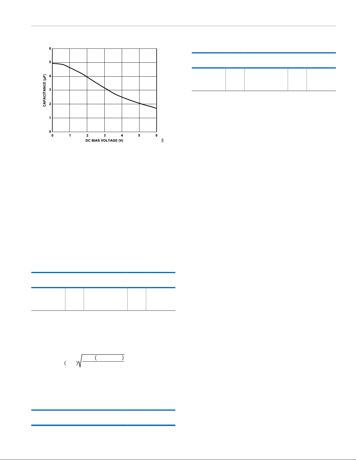
In this example, the worst-case temperature coefficient (TEMPCO)
over −40°C to +85°C is assumed to be 15% for an X5R dielectric.
The tolerance of the capacitor (TOL) is assumed to be 10%, and
C
is 4.0466 μF at 1.8 V, as shown in Figure 35.
OUT
Substituting these values in the equation yields
C
= 4.0466 μF × (1 − 0.15) × (1 − 0.1) = 3.0956 μF
EFF
To guarantee the performance of the ADP2138/ADP2139, it is
imperative that the effects of dc bias, temperature, and tolerances
on the behavior of the capacitors be evaluated for each application.
× (1 − TEMPCO) × (1 − TOL)
(5)
(6)
analog.com Rev. E | 14 of 19
Page 15
Data Sheet ADP2138/ADP2139
APPLICATIONS INFORMATION
Table 8. Suggested 4.7 μF Capacitors (Continued)
Vendor Type Model
Murata X5R GRM188R60J475 0603 6.3
Taiyo Yuden X5R JMK107BJ475 0603 6.3
Coilcraft TDK X5R C1608X5R0J475 0603 6.3
THERMAL CONSIDERATIONS
Because of the high efficiency of the ADP2138/ADP2139, only a
small amount of power is dissipated inside the ADP2138/ADP2139
package, which reduces thermal constraints.
However, in applications with maximum loads at high ambient
temperature, low supply voltage, and high duty cycle, the heat
Figure 35. Typical Capacitor Performance
The peak-to-peak output voltage ripple for the selected output
capacitor and inductor values is calculated using the following
equation:
V
RIPPLE
= I
RIPPLE
× (ESR
+ 1/(8 × fSW × C
COUT
OUT
))
(7)
where:
V
is the allowable peak-to-peak output voltage ripple in Volts.
RIPPLE
I
is the inductor ripple current in Amperes.
RIPPLE
ESR
is the equivalent series resistance of the output capacitor
COUT
in Ohms.
Capacitors with lower equivalent series resistance (ESR) are recommended to produce low output ripple. The effective capacitance
needed for stability, which includes temperature and dc bias effects,
is 3 µF.
Table 7. Suggested 4.7 μF Capacitors
Case
Vendor Type Model
Murata X5R GRM188R60J475 0603 6.3
Taiyo Yuden X5R JMK107BJ475 0603 6.3
Coilcraft TDK X5R C1608X5R0J475 0603 6.3
Size
Voltage Rating
(V)
dissipated in the package is great enough that it may cause the
junction temperature of the die to exceed the maximum junction
temperature of 125°C. If the junction temperature exceeds 150°C,
the converter enters thermal shutdown. It recovers when the junction temperature falls below 130°C.
The junction temperature of the die is the sum of the ambient
temperature of the environment and the temperature rise of the
package due to power dissipation, as shown in the following equation:
TJ = TA + T
R
where:
TJ is the junction temperature.
TA is the ambient temperature.
TR is the rise in temperature of the package due to power dissipa-
tion.
The rise in temperature of the package is directly proportional to the
power dissipation in the package. The proportionality constant for
this relationship is the thermal resistance from the junction of the
die to the ambient temperature, as shown in the following equation:
TR = θJA × P
where:
TR is the rise in temperature of the package.
Input Capacitor
Higher value input capacitors help to reduce the input voltage ripple
and improve transient response. Maximum input capacitor current
is calculated using the following equation:
I
CIN
≥ I
LOAD MAX
V
OUTvIN
− V
OUT
V
IN
(8)
To minimize supply noise, place the input capacitor as close to
the VIN pin of the ADP2138/ADP2139 as possible. As with the
output capacitor, a low ESR capacitor is recommended. The list of
recommended capacitors is shown in Table 8.
Table 8. Suggested 4.7 μF Capacitors
Vendor Type Model
Case
Size
Voltage Rating
(V)
θJA is the thermal resistance from the junction of the die to the
ambient temperature of the package.
PD is the power dissipation in the package.
PCB LAYOUT GUIDELINES
Poor layout can affect ADP2138/ADP2139 performance, causing
EMI and electromagnetic compatibility problems, ground bounce,
and voltage losses. Poor layout can also affect regulation and
stability. To implement a good layout, use the following rules:
► Place the inductor, input capacitor, and output capacitor close
to the IC using short tracks. These components carry high
switching frequencies, and large tracks act as antennas.
► Route the output voltage path away from the inductor and SW
node to minimize noise and magnetic interference.
Case
Size
D
Voltage Rating
(V)
(9)
(10)
analog.com Rev. E | 15 of 19
Page 16

Data Sheet ADP2138/ADP2139
APPLICATIONS INFORMATION
► Maximize the size of ground metal on the component side to
help with thermal dissipation.
► Use a ground plane with several vias connecting to the compo-
nent side ground to further reduce noise interference on sensitive circuit nodes.
analog.com Rev. E | 16 of 19
Page 17
Data Sheet ADP2138/ADP2139
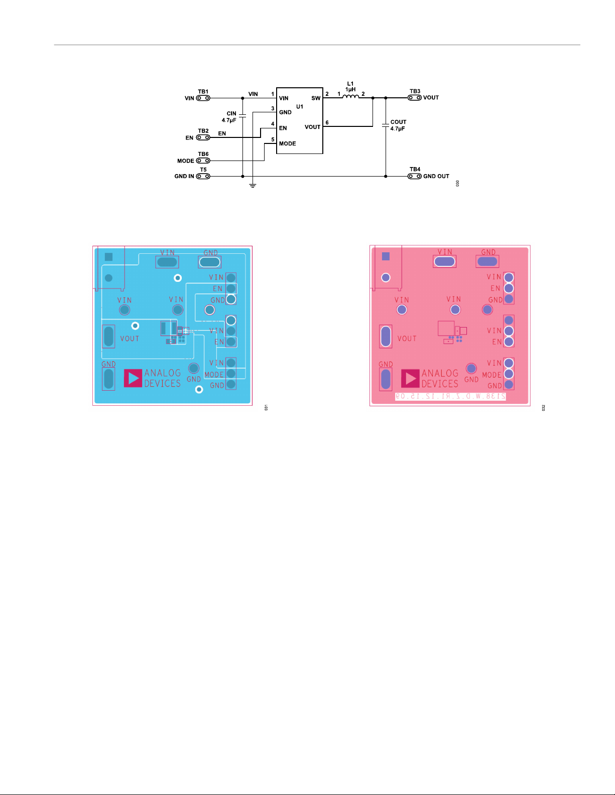
EVALUATION BOARD
Figure 36. Evaluation Board Schematic
EVALUATION BOARD LAYOUT
Figure 37. Top Layer
Figure 38. Bottom Layer
analog.com Rev. E | 17 of 19
Page 18

Data Sheet ADP2138/ADP2139
OUTLINE DIMENSIONS
Package Drawing (Option) Package Type Package Description
CB-6-12 WLCSP 6-Ball Wafer Level Chip Scale Package
For the latest package outline information and land patterns (footprints), go to Package Index.
ORDERING GUIDE
1
Model
ADP2138ACBZ-0.8-R7 −40°C to +125°C 6-Ball Wafer Level Chip Scale Package [WLCSP] Reel, 3000 CB-6-12 LJH
ADP2138ACBZ-1.0-R7 −40°C to +125°C 6-Ball Wafer Level Chip Scale Package [WLCSP] Reel, 3000 CB-6-12 L88
ADP2138ACBZ-1.2-R7 −40°C to +125°C 6-Ball Wafer Level Chip Scale Package [WLCSP] Reel, 3000 CB-6-12 L89
ADP2138ACBZ-1.5-R7 −40°C to +125°C 6-Ball Wafer Level Chip Scale Package [WLCSP] Reel, 3000 CB-6-12 L8A
ADP2138ACBZ-1.8-R7 −40°C to +125°C 6-Ball Wafer Level Chip Scale Package [WLCSP] Reel, 3000 CB-6-12 L8C
ADP2138ACBZ-2.5-R7 −40°C to +125°C 6-Ball Wafer Level Chip Scale Package [WLCSP] Reel, 3000 CB-6-12 L93
ADP2138ACBZ-2.8-R7 −40°C to +125°C 6-Ball Wafer Level Chip Scale Package [WLCSP] Reel, 3000 CB-6-12 LDH
ADP2138ACBZ-3.0-R7 −40°C to +125°C 6-Ball Wafer Level Chip Scale Package [WLCSP] Reel, 3000 CB-6-12 LDJ
ADP2138ACBZ-3.3-R7 −40°C to +125°C 6-Ball Wafer Level Chip Scale Package [WLCSP] Reel, 3000 CB-6-12 LDP
ADP2139ACBZ-0.8-R7 −40°C to +125°C 6-Ball Wafer Level Chip Scale Package [WLCSP] Reel, 3000 CB-6-12 LJJ
ADP2139ACBZ-1.0-R7 −40°C to +125°C 6-Ball Wafer Level Chip Scale Package [WLCSP] Reel, 3000 CB-6-12 LHN
ADP2139ACBZ-1.2-R7 −40°C to +125°C 6-Ball Wafer Level Chip Scale Package [WLCSP] Reel, 3000 CB-6-12 LHP
ADP2139ACBZ-1.5-R7 −40°C to +125°C 6-Ball Wafer Level Chip Scale Package [WLCSP] Reel, 3000 CB-6-12 LHQ
ADP2139ACBZ-1.8-R7 −40°C to +125°C 6-Ball Wafer Level Chip Scale Package [WLCSP] Reel, 3000 CB-6-12 LHR
ADP2139ACBZ-2.5-R7 −40°C to +125°C 6-Ball Wafer Level Chip Scale Package [WLCSP] Reel, 3000 CB-6-12 LHS
ADP2139ACBZ-2.8-R7 −40°C to +125°C 6-Ball Wafer Level Chip Scale Package [WLCSP] Reel, 3000 CB-6-12 LHT
ADP2139ACBZ-3.0-R7 −40°C to +125°C 6-Ball Wafer Level Chip Scale Package [WLCSP] Reel, 3000 CB-6-12 LHU
ADP2139ACBZ-3.3-R7 −40°C to +125°C 6-Ball Wafer Level Chip Scale Package [WLCSP]
1
Z = RoHS Compliant Part.
Temperature Range Package Description Packing Quantity
Reel, 3000
Package
Option Marking Code
CB-6-12 LHV
OUTPUT VOLTAGE OPTION
1
Model
ADP2138ACBZ-0.8-R7 0.8
ADP2138ACBZ-1.0-R7 1.0
ADP2138ACBZ-1.2-R7 1.2
ADP2138ACBZ-1.5-R7 1.5
ADP2138ACBZ-1.8-R7 1.8
ADP2138ACBZ-2.5-R7 2.5
ADP2138ACBZ-2.8-R7 2.8
ADP2138ACBZ-3.0-R7 3.0
ADP2138ACBZ-3.3-R7 3.3
ADP2139ACBZ-0.8-R7 0.8
ADP2139ACBZ-1.0-R7 1.0
ADP2139ACBZ-1.2-R7 1.2
ADP2139ACBZ-1.5-R7 1.5
ADP2139ACBZ-1.8-R7 1.8
ADP2139ACBZ-2.5-R7 2.5
ADP2139ACBZ-2.8-R7 2.8
ADP2139ACBZ-3.0-R7 3.0
ADP2139ACBZ-3.3-R7 3.3
analog.com Rev. E | 18 of 19
Output Voltage (V)
Page 19

Data Sheet ADP2138/ADP2139
OUTLINE DIMENSIONS
1
Z = RoHS Compliant Part.
EVALUATION BOARDS
1
Model
ADP2138CB-0.8EVALZ Evaluation Board
ADP2138CB-1.0EVALZ Evaluation Board
ADP2138CB-1.2EVALZ Evaluation Board
ADP2138CB-1.5EVALZ Evaluation Board
ADP2138CB-1.8EVALZ Evaluation Board
ADP2138CB-2.5EVALZ Evaluation Board
ADP2138CB-2.8EVALZ Evaluation Board
ADP2138CB-3.0EVALZ Evaluation Board
ADP2138CB-3.3EVALZ Evaluation Board
ADP2139CB-0.8EVALZ Evaluation Board
ADP2139CB-1.0EVALZ Evaluation Board
ADP2139CB-1.2EVALZ Evaluation Board
ADP2139CB-1.5EVALZ Evaluation Board
ADP2139CB-1.8EVALZ Evaluation Board
ADP2139CB-2.5EVALZ Evaluation Board
ADP2139CB-3.0EVALZ Evaluation Board
ADP2139CB-3.3EVALZ Evaluation Board
Description
1
Z = RoHS Compliant Part.
©2011-2025 Analog Devices, Inc. All rights reserved. Trademarks and
registered trademarks are the property of their respective owners.
One Analog Way, Wilmington, MA 01887-2356, U.S.A.
Rev. E | 19 of 19
 Loading...