

Page 1
with 10-Bit DACs
AD9958
Rev. C Document Feedback
Trademarks and registered trademarks are the property of their respective owners.
Technical Support www.analog.com
RECONSTRUCTED
SINE WAVE
10-BIT
DAC
RECONSTRUCTED
SINE WAVE
10-BIT
DAC
(2)
500MSPS
DDS CORES
TIMING AND
CONTROL
USER INTERF ACE
MODULATION CONTROL
REF CLOCK
INPUT CIRCUI TRY
SYSTEM
CLOCK
SOURCE
AD9958
05252-000
Data Sheet
FEATURES
2 synchronized DDS channels @ 500 MSPS
Independent frequency/phase/amplitude control between
channels
Matched latencies for frequency/phase/amplitude changes
Excellent channel-to-channel isolation (>72 dB)
Linear frequency/phase/amplitude sweeping capability
Up to 16 levels of frequency/phase/amplitude modulation
(pin-selectable)
2 integrated 10-bit digital-to-analog converters (DACs)
Individually programmable DAC full-scale currents
0.12 Hz or better frequency tuning resolution
14-bit phase offset resolution
10-bit output amplitude scaling resolution
Serial I/O port interface (SPI) with 800 Mbps data throughput
Software-/hardware-controlled power-down
Dual supply operation (1.8 V DDS core/3.3 V serial I/O)
Multiple device synchronization
Selectable 4× to 20× REFCLK multiplier (PLL)
Selectable REFCLK crystal oscillator
56-lead LFCSP
2-Channel, 500 MSPS DDS
APPLICATIONS
Agile local oscillators
Phased array radars/sonars
Instrumentation
Synchronized clocking
RF source for AOTF
Single-side band suppressed carriers
Quadrature communications
Information furnishe d by Analog Devices is believed to be accurate and reliable. However, no
responsibility is assumed by Analog Devices for its use, nor for any infringements of patents or other
rights of third parties that may result from its use. Specifications subject to change without notice. No
license is granted by implication or otherwise under any patent or patent rights of Analog Devices.
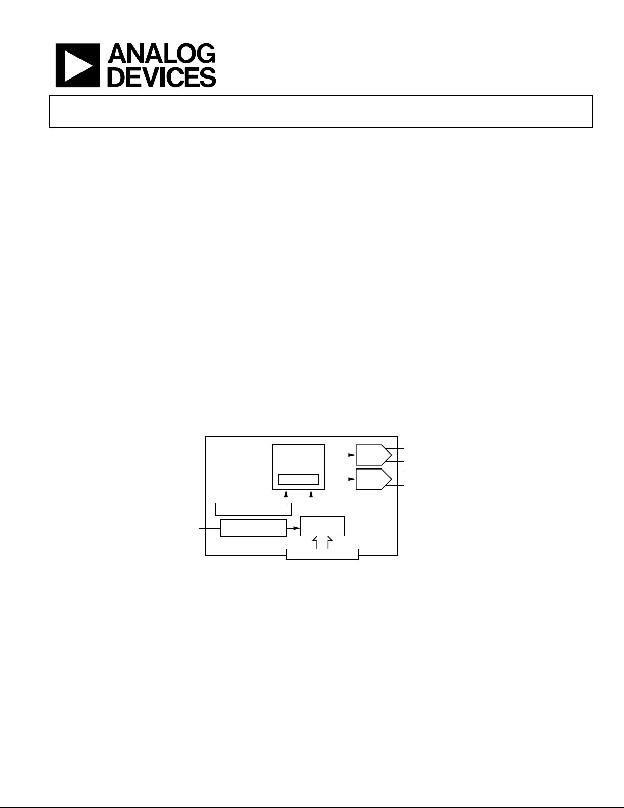
FUNCTIONAL BLOCK DIAGRAM
Figure 1.
One Technology Way, P.O. Box 9106, Norwood, MA 02062-9106, U.S.A.
Tel: 781.329.4700 ©2005–2016 Analog Devices, Inc. All rights reserved.
Page 2

AD9958 Data Sheet
TABLE OF CONTENTS
Features .............................................................................................. 1
Applications ....................................................................................... 1
Functional Block Diagram .............................................................. 1
Revision History ............................................................................... 2
General Description ......................................................................... 3
Specifications ..................................................................................... 4
Absolute Maximum Ratings ............................................................ 8
ESD Caution .................................................................................. 8
Pin Configuration and Function Descriptions ............................. 9
Typical Performance Characteristics ........................................... 11
Application Circuits ....................................................................... 14
Equivalent Input and Output Circuits ......................................... 17
Theory of Operation ...................................................................... 18
DDS Core ..................................................................................... 18
Digital-to-Analog Converter .................................................... 18
Modes of Operation ....................................................................... 19
Channel Constraint Guidelines ................................................ 19
Power Supplies ............................................................................ 19
Single-Tone Mo d e ...................................................................... 19
Reference Clock Modes ............................................................. 20
Scalable DAC Reference Current Control Mode ................... 21
Power-Down Functions ............................................................. 21
Modulation Mode ....................................................................... 21
Modulation Using SDIO_x Pins for RU/RD .......................... 24
Linear Sweep Mode .................................................................... 25
Linear Sweep No-Dwell Mode ................................................. 26
Sweep and Phase Accumulator Clearing Functions .............. 27
Output Amplitude Control Mode ............................................ 28
Synchronizing Multiple AD9958 Devices ................................... 29
Automatic Mode Synchronization ........................................... 29
Manual Software Mode Synchronization ................................ 29
Manual Hardware Mode Synchronization .............................. 29
I/O_UPDATE, SYNC_CLK, and System Clock
Relationships ............................................................................... 30
Serial I/O Port ................................................................................. 31
Overview ..................................................................................... 31
Instruction Byte Description .................................................... 32
Serial I/O Port Pin Description ................................................ 32
Serial I/O Port Function Description ...................................... 32
MSB/LSB Transfer Description ................................................ 32
Serial I/O Modes of Operation ................................................. 33
Register Maps and Bit Descriptions ............................................. 36
Register Maps .............................................................................. 36
Descriptions for Control Registers .......................................... 39
Descriptions for Channel Registers ......................................... 41
Outline Dimensions ....................................................................... 44
Ordering Guide .......................................................................... 44
REVISION HISTORY
11/2016—Rev. B to Rev. C
Change to Figure 37 Caption ........................................................ 26
4/2013—Rev. A to Rev. B
Changes to Linear Sweep Mode Section and Setting the Slope of
the Linear Sweep ............................................................................. 25
Changes to Figure 38 and Figure 39 Captions ............................ 27
Changes to Ramp Rate Timer Section ......................................... 28
Updated Outline Dimensions ....................................................... 44
7/2008—Rev. 0 to Rev. A
Changes to Features .......................................................................... 1
Inserted Figure 1; Renumbered Sequentially ................................ 1
Changes to Input Level Parameter i n Ta bl e 1 ............................... 4
Added Profile Pin Toggle Rate Parameter in Table 1 ................... 6
Changes to Layout ............................................................................ 8
Changes to Table 3 ............................................................................ 9
Added Equivalent Input and Output Circuits Section .............. 17
Changes to Reference Clock Input Circuitry Section ................ 20
Rev. C | Page 2 of 44
Change to Figure 35 ....................................................................... 21
Changes to Setting the Slope of the Linear Sweep Section ....... 25
Changes to Figure 37...................................................................... 26
Changes to Figure 38 and Figure 39 ............................................ 27
Changes to Figure 40...................................................................... 30
Added Table 25; Renumbered Sequentially ................................ 31
Changes to Figure 41...................................................................... 31
Changes to Figure 42, Serial Data I/O (SDIO_0, SDIO_1,
SDIO_3) Section, and Added Example Instruction Byte
Section .............................................................................................. 32
Added Table 27 ............................................................................... 33
Changes to Figure 46, Figure 47, Figure 48, and Figure 49 ...... 35
Changes to Register Maps and Bit Descriptions Section and
Added Endnote 2 to Table 28 ........................................................ 36
Added Endnote 1 to Table 30 ........................................................ 38
Added Exposed Pad Notation to Outline Dimensions ............. 44
9/2005—Revision 0: Initial Version
Page 3
Data Sheet AD9958
GENERAL DESCRIPTION
The AD9958 consists of two DDS cores that provide independent frequency, phase, and amplitude control on each channel.
This flexibility can be used to correct imbalances between
signals due to analog processing, such as filtering, amplification,
or PCB layout related mismatches. Because both channels share
a common system clock, they are inherently synchronized.
Synchronization of multiple devices is supported.
The AD9958 can perform up to a 16-level modulation of
frequency, phase, or amplitude (FSK, PSK, ASK). Modulation is
performed by applying data to the profile pins. In addition, the
AD9958 also supports linear sweep of frequency, phase, or
amplitude for applications such as radar and instrumentation.
The AD9958 serial I/O port offers multiple configurations to
provide significant flexibility. The serial I/O port offers an SPIcompatible mode of operation that is virtually identical to the
SPI operation found in earlier Analog Devices, Inc., DDS
products. Flexibility is provided by four data pins (SDIO_0/
SDIO_1/SDIO_2/SDIO_3) that allow four programmable
modes of serial I/O operation.
The AD9958 uses advanced DDS technology that provides low
power dissipation with high performance. The device incorporates
two integrated, high speed 10-bit DACs with excellent wideband
and narrow-band SFDR. Each channel has a dedicated 32-bit
frequency tuning word, 14 bits of phase offset, and a 10-bit
output scale multiplier.
The DAC outputs are supply referenced and must be terminated into AVDD by a resistor or an AVDD center-tapped
transformer. Each DAC has its own programmable reference to
enable different full-scale currents for each channel.
The DDS acts as a high resolution frequency divider with the
REFCLK as the input and the DAC providing the output. The
REFCLK input source is common to both channels and can be
driven directly or used in combination with an integrated
REFCLK multiplier (PLL) up to a maximum of 500 MSPS. The
PLL multiplication factor is programmable from 4 to 20, in
integer steps. The REFCLK input also features an oscillator
circuit to support an external crystal as the REFCLK source.
The crystal must be between 20 MHz and 30 MHz. The crystal
can be used in combination with the REFCLK multiplier.
The AD9958 comes in a space-saving 56-lead LFCSP package.
The DDS core (AVDD and DVDD pins) is powered by a 1.8 V
supply. The digital I/O interface (SPI) operates at 3.3 V and
requires the pin labeled DVDD_I/O (Pin 49) be connected
to 3.3 V.
The AD9958 operates over the industrial temperature range of
−40°C to +85°C.
SYNC_IN
SYNC_OUT
I/O_UPDATE
SYNC_CL K
REF_CLK
REF_CLK
AD9958
∆FTW
BUFFER /
XTAL
OSCILLATOR
CLK_MODE_SEL
Σ Σ Σ
32 32 1015
Σ Σ Σ
32
FTW
÷4
REF CLOCK
MULTIPLIER
32
32 PHASE/
4× TO 20×
∆PHASE
TIMING AND CONTROL L OGIC
SYSTEM
CLK
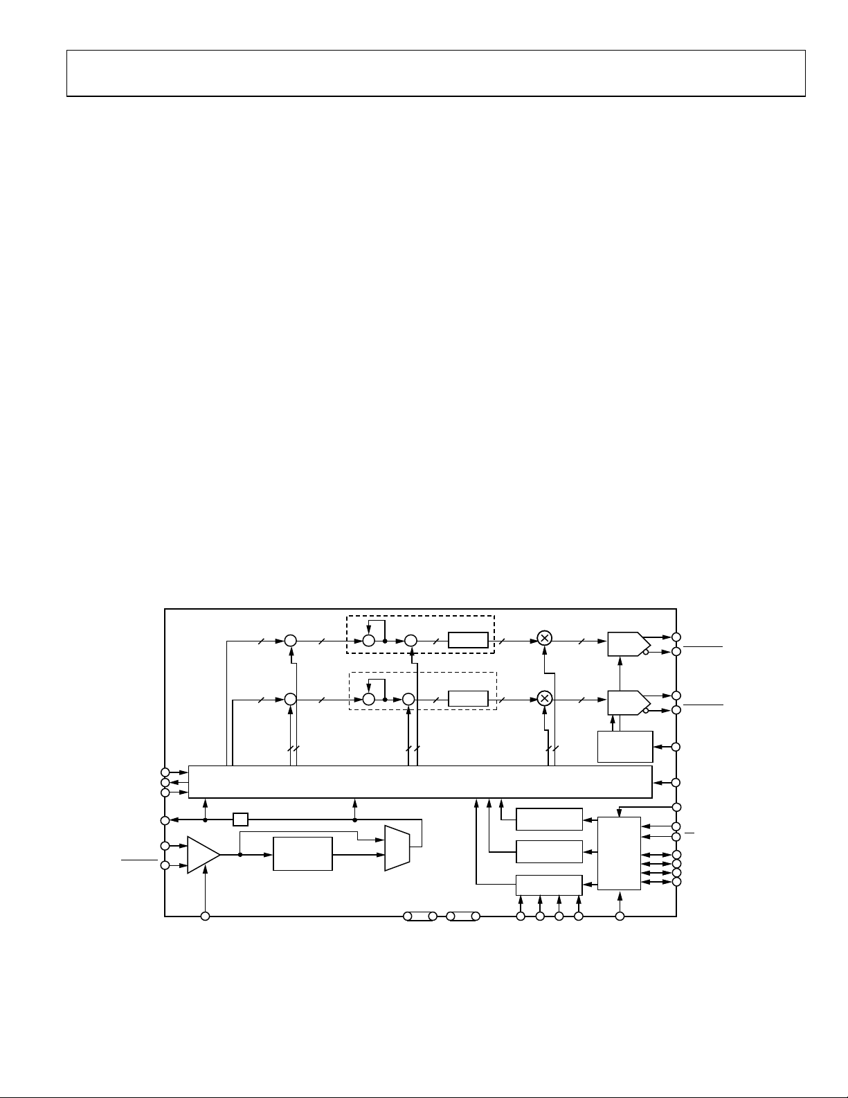
Figure 2. Detailed Block Diagram
MUX
1.8V
AVDD DVDD
C
O
S
D
D
R
COS(X)
DDS CORE
COS(X)
1.8V
E
1015
AMP/
∆AMP
CONTRO L
REGISTERS
C
H
A
N
R
E
S
I
G
PROFILE
REGISTERS
P0 P1 P2 P3 DVDD_I/O
DAC
10
DAC
10
SCALABLE
1014
N
L
E
E
T
R
DAC REF
CURRENT
I/O
PORT
S
BUFFER
CH0_IOUT
CH0_IOUT
CH1_IOUT
CH1_IOUT
DAC_RSET
PWR_DWN_CTL
MASTER_RESET
SCLK
CS
SDIO_0
SDIO_1
SDIO_2
SDIO_3
05252-001
Rev. C | Page 3 of 44
Page 4

AD9958 Data Sheet
150 MHz to 200 MHz Analog Output
−53 dBc
15.1 MHz Analog Output (±1 MHz)
−83 dBc
SPECIFICATIONS
AVDD and DVDD = 1.8 V ± 5%; DVDD_I/O = 3.3 V ± 5%; T = 25°C; R
(REFCLK multiplier bypassed), unless otherwise noted.
Table 1.
Parameter Min Typ Max Unit Test Conditions/Comments
REFERENCE CLOCK INPUT CHARACTERISTICS
Frequency Range
REFCLK Multiplier Bypassed 1 500 MHz
REFCLK Multiplier Enabled 10 125 MHz
Internal VCO Output Frequency Range
VCO Gain Control Bit Set High1 255 500 MHz
VCO Gain Control Bit Set Low1
Crystal REFCLK Source Range 20 30 MHz
Input Level 200 1000 mV Measured at each pin (single-ended)
Input Voltage Bias Level 1.15 V
Input Capacitance 2 pF
Input Impedance 1500 Ω
Duty Cycle with REFCLK Multiplier Bypassed 45 55 %
Duty Cycle with REFCLK Multiplier Enabled 35 65 %
CLK Mode Select (Pin 24) Logic 1 Voltage 1.25 1.8 V 1.8 V digital input logic
CLK Mode Select (Pin 24) Logic 0 Voltage 0.5 V 1.8 V digital input logic
DAC OUTPUT CHARACTERISTICS Must be referenced to AVDD
Resolution 10 Bits
Full-Scale Output Current 1.25 10 mA
Gain Error −10 +10 % FS
Channel-to-Channel Output Amplitude Matching Error −2.5 +2.5 %
Output Current Offset 1 25 µA
Differential Nonlinearity ±0.5 LSB
Integral Nonlinearity ±1.0 LSB
Output Capacitance 3 pF
Voltage Compliance Range AVDD −
Channel-to-Channel Isolation 72 dB
WIDEBAND SFDR The frequency range for wideband SFDR
1 MHz to 20 MHz Analog Output −65 dBc
20 MHz to 60 MHz Analog Output −62 dBc
60 MHz to 100 MHz Analog Output −59 dBc
100 MHz to 150 MHz Analog Output −56 dBc
100 160 MHz
AVDD +
0.50
= 1.91 kΩ; external reference clock frequency = 500 MSPS
SET
See
Figure 34 and Figure 35
0.50
V
DAC supplies tied together (see
is defined as dc to Nyquist
Figure 19)
NARROW-BAND SFDR
1.1 MHz Analog Output (±10 kHz) −90 dBc
1.1 MHz Analog Output (±50 kHz) −88 dBc
1.1 MHz Analog Output (±250 kHz) −86 dBc
1.1 MHz Analog Output (±1 MHz) −85 dBc
15.1 MHz Analog Output (±10 kHz) −90 dBc
15.1 MHz Analog Output (±50 kHz) −87 dBc
15.1 MHz Analog Output (±250 kHz) −85 dBc
40.1 MHz Analog Output (±10 kHz) −90 dBc
40.1 MHz Analog Output (±50 kHz) −87 dBc
40.1 MHz Analog Output (±250 kHz) −84 dBc
40.1 MHz Analog Output (±1 MHz) −82 dBc
75.1 MHz Analog Output (±10 kHz) −87 dBc
Rev. C | Page 4 of 44
Page 5
Data Sheet AD9958
200.3 MHz Analog Output (±10 kHz)
−87 dBc
@ 1 MHz Offset
−165 dBc/Hz
@ 10 kHz Offset
−144 dBc/Hz
@ 1 kHz Offset
−139 dBc/Hz
@ 100 kHz Offset
−145 dBc/Hz
@ 10 kHz Offset
−134 dBc/Hz
@ 1 kHz Offset
−120 dBc/Hz
Parameter Min Typ Max Unit Test Conditions/Comments
75.1 MHz Analog Output (±50 kHz) −85 dBc
75.1 MHz Analog Output (±250 kHz) −83 dBc
75.1 MHz Analog Output (±1 MHz) −82 dBc
100.3 MHz Analog Output (±10 kHz) −87 dBc
100.3 MHz Analog Output (±50 kHz) −85 dBc
100.3 MHz Analog Output (±250 kHz) −83 dBc
100.3 MHz Analog Output (±1 MHz) −81 dBc
200.3 MHz Analog Output (±50 kHz) −85 dBc
200.3 MHz Analog Output (±250 kHz) −83 dBc
200.3 MHz Analog Output (±1 MHz) −81 dBc
PHASE NOISE CHARACTERISTICS
Residual Phase Noise @ 15.1 MHz (f
@ 1 kHz Offset −150 dBc/Hz
@ 10 kHz Offset −159 dBc/Hz
@ 100 kHz Offset −165 dBc/Hz
)
OUT
Residual Phase Noise @ 40.1 MHz (f
)
OUT
@ 1 kHz Offset −142 dBc/Hz
@ 10 kHz Offset −151 dBc/Hz
@ 100 kHz Offset −160 dBc/Hz
@ 1 MHz Offset −162 dBc/Hz
Residual Phase Noise @ 75.1 MHz (f
)
OUT
@ 1 kHz Offset −135 dBc/Hz
@ 10 kHz Offset −146 dBc/Hz
@ 100 kHz Offset −154 dBc/Hz
@ 1 MHz Offset −157 dBc/Hz
Residual Phase Noise @ 100.3 MHz (f
)
OUT
@ 1 kHz Offset −134 dBc/Hz
@ 100 kHz Offset −152 dBc/Hz
@ 1 MHz Offset −154 dBc/Hz
Residual Phase Noise @ 15.1 MHz (f
Multiplier Enabled 5×
) with REFCLK
OUT
@ 10 kHz Offset −149 dBc/Hz
@ 100 kHz Offset −153 dBc/Hz
@ 1 MHz Offset −148 dBc/Hz
Residual Phase Noise @ 40.1 MHz (f
Multiplier Enabled 5×
) with REFCLK
OUT
@ 1 kHz Offset −130 dBc/Hz
@ 10 kHz Offset −140 dBc/Hz
@ 1 MHz Offset −139 dBc/Hz
Residual Phase Noise @ 75.1 MHz (f
Multiplier Enabled 5×
@ 1 kHz Offset −123 dBc/Hz
@ 100 kHz Offset −138 dBc/Hz
@ 1 MHz Offset −132 dBc/Hz
Residual Phase Noise @ 100.3 MHz (f
Multiplier Enabled 5×
@ 10 kHz Offset −130 dBc/Hz
@ 100 kHz Offset −135 dBc/Hz
@ 1 MHz Offset −129 dBc/Hz
) with REFCLK
OUT
) with REFCLK
OUT
Rev. C | Page 5 of 44
Page 6

AD9958 Data Sheet
Residual Phase Noise @ 75.1 MHz (f
) with REFCLK
@ 1 MHz Offset
−123 dBc/Hz
Minimum Hold Time (Profile Inputs to SYNC_CLK)
0
ns
Logic 1 Current
3
12
µA
VOH
2.7
V
Parameter Min Typ Max Unit Test Conditions/Comments
Residual Phase Noise @ 15.1 MHz (f
Multiplier Enabled 20×
@ 1 kHz Offset −127 dBc/Hz
@ 10 kHz Offset −136 dBc/Hz
@ 100 kHz Offset −139 dBc/Hz
@ 1 MHz Offset −138 dBc/Hz
Residual Phase Noise @ 40.1 MHz (f
Multiplier Enabled 20×
@ 1 kHz Offset −117 dBc/Hz
@ 10 kHz Offset −128 dBc/Hz
@ 100 kHz Offset −132 dBc/Hz
@ 1 MHz Offset −130 dBc/Hz
Multiplier Enabled 20×
@ 1 kHz Offset −110 dBc/Hz
@ 10 kHz Offset −121 dBc/Hz
@ 100 kHz Offset −125 dBc/Hz
) with REFCLK
OUT
) with REFCLK
OUT
OUT
Residual Phase Noise @ 100.3 MHz (f
Multiplier Enabled 20×
) with REFCLK
OUT
@ 1 kHz Offset −107 dBc/Hz
@ 10 kHz Offset −119 dBc/Hz
@ 100 kHz Offset −121 dBc/Hz
@ 1 MHz Offset −119 dBc/Hz
SERIAL PORT TIMING CHARACTERISTICS
Maximum Frequency Serial Clock (SCLK) 200 MHz
Minimum SCLK Pulse Width Low (t
Minimum SCLK Pulse Width High (t
) 1.6 ns
PWL
) 2.2 ns
PWH
Minimum Data Setup Time (tDS) 2.2 ns
Minimum Data Hold Time 0 ns
Minimum CS Setup Time (t
)
PRE
1.0 ns
Minimum Data Valid Time for Read Operation 12 ns
MISCELLANEOUS TIMING CHARACTERISTICS
MASTER_RESET Minimum Pulse Width 1 Min pulse width = 1 sync clock period
I/O_UPDATE Minimum Pulse Width 1 Min pulse width = 1 sync clock period
Minimum Setup Time (I/O_UPDATE to SYNC_CLK) 4.8 ns Rising edge to rising edge
Minimum Hold Time (I/O_UPDATE to SYNC_CLK) 0 ns Rising edge to rising edge
Minimum Setup Time (Profile Inputs to SYNC_CLK) 5.4 ns
Minimum Setup Time (SDIO Inputs to SYNC_CLK) 2.5 ns
Minimum Hold Time (SDIO Inputs to SYNC_CLK) 0 ns
Propagation Time Between REF_CLK and SYNC_CLK 2.25 3.5 5.5 ns
Profile Pin Toggle Rate 2 Sync
clocks
CMOS LOGIC INPUTS
VIH 2.0 V
VIL 0.8 V
Logic 0 Current −12 µA
Input Capacitance 2 pF
CMOS LOGIC OUTPUTS 1 mA load
VOL 0.4 V
Rev. C | Page 6 of 44
Page 7

Data Sheet AD9958
I
Power-Down Mode
2.5
mA
Frequency Word to DAC Output with Matched
29
SYSCLKs
Phase Offset Word to DAC Output
29
SYSCLKs
Parameter Min Typ Max Unit Test Conditions/Comments
POWER SUPPLY
Total Power Dissipation—Both Channels On, Single-
Tone Mode
Total Power Dissipation—Both Channels On, with
Sweep Accumulator
Total Power Dissipation—Full Power-Down 13 mW
I
—Both Channels On, Single-Tone Mode 90 105 mA
AVDD
I
—Both Channels On, Sweep Accumulator,
AVDD
REFCLK Multiplier, and 10-Bit Output Scalar
Enabled
I
—Both Channels On, Single-Tone Mode 60 70 mA
DVDD
I
—Both Channels On, Sweep Accumulator,
DVDD
REFCLK Multiplier, and 10-Bit Output Scalar
Enabled
I
22 mA I
DVDD_I/O
30 mA I
I
Power-Down Mode 2.5 mA
AVDD
DVDD
DATA LATENCY (PIPELINE DELAY) SINGLE-TONE MODE
Frequency, Phase, and Amplitude Words to DAC
Output with Matched Latency Enabled
Latency Disabled
Phase Offset Word to DAC Output with Matched
Latency Disabled
Amplitude Word to DAC Output with Matched
Latency Disabled
DATA LATENCY (PIPELINE DELAY) MODULATION MODE
Frequency Word to DAC Output 34 SYSCLKs
315 380 mW Dominated by supply variation
350 420 mW Dominated by supply variation
95 110 mA
70 80 mA
= read
DVDD
= write
DVDD
2, 3
29 SYSCLKs
25 SYSCLKs
17 SYSCLKs
3, 4
Amplitude Word to DAC Output 21 SYSCLKs
3, 4
DATA LATENCY (PIPELINE DELAY) LINEAR SWEEP MODE
Frequency Rising/Falling Delta-Tuning Word to DAC
41 SYSCLKs
Output
Phase Offset Rising/Falling Delta-Tuning Word to
37 SYSCLKs
DAC Output
Amplitude Rising/Falling Delta-Tuning Word to DAC
29 SYSCLKs
Output
1
For the VCO frequency range of 160 MHz to 255 MHz, there is no guarantee of operation.
2
Data latency is referenced to I/O_UPDATE.
3
Data latency is fixed.
4
Data latency is referenced to a profile change.
Rev. C | Page 7 of 44
Page 8
AD9958 Data Sheet
Lead Temperature (10 sec Soldering)
300°C
ABSOLUTE MAXIMUM RATINGS
Table 2.
Parameter Rating
Maximum Junction Temperature 150°C
DVDD_I/O (Pin 49) 4 V
AVDD, DVDD 2 V
Digital Input Voltage (DVDD_I/O = 3.3 V) −0.7 V to +4 V
Digital Output Current 5 mA
Storage Temperature Range –65°C to +150°C
Operating Temperature Range –40°C to +85°C
θJA 21°C/W
θJC 2°C/W
Stresses at or above those listed under Absolute Maximum
Ratings may cause permanent damage to the product. This is a
stress rating only; functional operation of the product at these
or any other conditions above those indicated in the operational
section of this specification is not implied. Operation beyond
the maximum operating conditions for extended periods may
affect product reliability.
ESD CAUTION
Rev. C | Page 8 of 44
Page 9
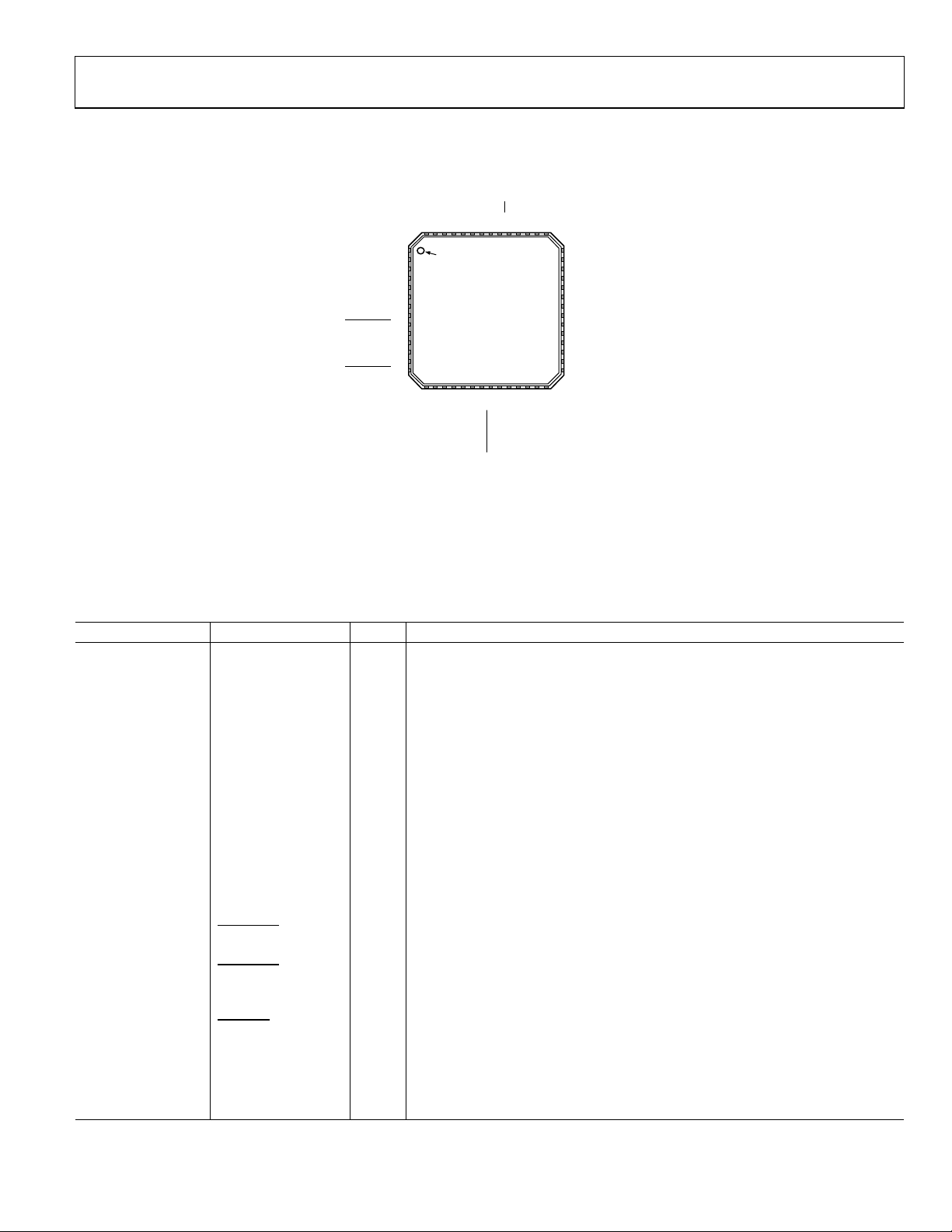
Data Sheet AD9958
3
MASTER_RESET
I
Active High Reset Pin. Asserting the MASTER_RESET pin forces the AD9958 internal
8
CH0_IOUT
O
True DAC Output. Terminates into AVDD.
PIN 1
INDICATOR
1
SYNC_IN
2
SYNC_OUT
3
MASTER_RESET
4
PWR_DWN_CTL
5
AVDD
6
AGND
7
AVDD
8
CH0_IOUT
9
CH0_IOUT
10
AGND
11
AVDD
12
AGND
13
CH1_IOUT
14
CH1_IOUT
35
AVDD
36
AVDD
37
AVDD
38
NC
39
AVDD
40
P0
41 P1
42
P2
34
NC
33
AVDD
32 NC
31 AVDD
30 AVDD
29
AVDD
15
AVDD
16
AGND
17
DAC_RSET
19
AVDD
21
AVDD
20
AGND
22
REF_CLK
23
REF_CLK
24
CLK_MODE_SEL
25
AGND
26
AVDD
27
LOOP_FILTER
28
NC
18
AGND
45
DVDD46I/O_UPDATE
47
CS
48
SCLK
49
DVDD_I/O
50
SDIO_0
51
SDIO_152SDIO_2
53
SDIO_3
54
SYNC_CLK
44
DGND
43
P3
TOP VIEW
(Not to S cale)
AD9958
55
DVDD
56
DGND
NOTES
1. THE EXPOSED EPAD ON BOTTOM SIDE OF PACKAGE IS AN
ELECTRICAL CONNECTION AND MUST BE SO LDERED TO G ROUND.
2. PIN 49 IS DVDD_I /O AND IS TIED TO 3.3V .
3. NC = NO CONNECT.
05252-005
PIN CONFIGURATION AND FUNCTION DESCRIPTIONS
Figure 3. Pin Configuration
Table 3. Pin Function Descriptions
Pin No. Mnemonic I/O1 Description
1 SYNC_IN I Used to Synchronize Multiple AD9958 Devices. Connects to the SYNC_OUT pin of
the master AD9958 device.
2 SYNC_OUT O Used to Synchronize Multiple AD9958 Devices. Connects to the SYNC_IN pin of the
slave AD9958 devices.
registers to their default state, as described in the Register Maps and Bit Descriptions
section.
4 PWR_DWN_CTL I External Power-Down Control.
5, 7, 11, 15, 19, 21,
AVDD I Analog Power Supply Pins (1.8 V).
26, 29, 30, 31, 33,
35, 36, 37, 39
6, 10, 12, 16, 18,
AGND I Analog Ground Pins.
20, 25
45, 55 DVDD I Digital Power Supply Pins (1.8 V).
44, 56 DGND I Digital Power Ground Pins.
9
13 CH1_IOUT O True DAC Output. Terminates into AVDD.
14
17 DAC_RSET I Establishes the Reference Current for All DACs. A 1.91 kΩ resistor (nominal) is
22
23 REF_CLK I Reference Clock/Oscillator Input. When the REF_CLK is operated in single-ended
CH0_IOUT
CH1_IOUT
REF_CLK
O Complementary DAC Output. Terminates into AVDD.
O Complementary DAC Output. Terminates into AVDD.
connected from Pin 17 to AGND.
I Complementary Reference Clock/Oscillator Input. When the REF_CLK is operated
in single-ended mode, this pin should be decoupled to AVDD or AGND with a
0.1 µF capacitor.
mode, this is the input. See the Modes of Operation section for the reference clock
configuration.
Rev. C | Page 9 of 44
Page 10
AD9958 Data Sheet
50
SDIO_0
I/O
Data Pin SDIO_0 is dedicated to the serial port I/O only.
Pin No. Mnemonic I/O1 Description
24 CLK_MODE_SEL I Control Pin for the Oscillator Section. Caution: Do not drive this pin beyond 1.8 V.
When high (1.8 V), the oscillator section is enabled to accept a crystal as the
REF_CLK source. When low, the oscillator section is bypassed.
27 LOOP_FILTER I Connects to the external zero compensation network of the PLL loop filter.
Typically, the network consists of a 0 Ω resistor in series with a 680 pF capacitor
tied to AVDD.
28, 32, 34, 38 NC N/A No Connection.
40, 41, 42, 43 P0, P1, P2, P3 I Data pins used for modulation (FSK, PSK, ASK), to start/stop for the sweep
accumulators, or used to ramp up/ramp down the output amplitude. The data is
synchronous to the SYNC_CLK (Pin 54). The data inputs must meet the setup and
hold time requirements to the SYNC_CLK. The functionality of these pins is
controlled by profile pin configuration (PPC) bits (FR1[14:12]).
46 I/O_UPDATE I A rising edge transfers data from the serial I/O port buffer to active registers.
I/O_UPDATE is synchronous to the SYNC_CLK (Pin 54). I/O_UPDATE must meet the
setup and hold time requirements to the SYNC_CLK to guarantee a fixed pipeline
delay of data to the DAC output; otherwise, a ±1 SYNC_CLK period of pipeline
uncertainty exists. The minimum pulse width is one SYNC_CLK period.
47
CS
48 SCLK I Serial Data Clock for I/O Operations. Data bits are written on the rising edge of
49 DVDD_I/O I 3.3 V Digital Power Supply for SPI Port and Digital I/O.
I Active Low Chip Select. Allows multiple devices to share a common I/O bus (SPI).
SCLK and read on the falling edge of SCLK.
51, 52, 53 SDIO_1, SDIO_2,
SDIO_3
I/O Data Pin SDIO_1, Data Pin SDIO_2, and Data Pin SDIO_3 can be used for the serial
I/O port or used to initiate a ramp-up/ramp-down (RU/RD) of the DAC output
amplitude.
54 SYNC_CLK O The SYNC_CLK runs at one fourth the system clock rate. It can be disabled. I/O_UPDATE
or data (Pin 40 to Pin 43) is synchronous to the SYNC_CLK. To guarantee a fixed
pipeline delay of data to DAC output, I/O_UPDATE or data (Pin 40 to Pin 43) must
meet the setup and hold time requirements to the rising edge of SYNC_CLK;
otherwise, a ±1 SYNC_CLK period of uncertainty exists.
1
I = input, O = output.
Rev. C | Page 10 of 44
Page 11
Data Sheet AD9958
0
–100
(dB)
–10
–20
–30
–40
–50
–60
–70
–80
–90
START 0Hz
S
TOP 250MHz25MHz/DIV
DE
LT
A
1 (T1)
–71.73dB
4.50901804MHz
RBW
20kHz
RF
A
TT
20dB
VBW
20kHz
SWT 1.6s
UNIT
dB
REF LVL
0dBm
A
1AP
05252-006
0
–100
(dB)
–10
–20
–30
–40
–50
–60
–70
–80
–90
START 0Hz
STOP 250Hz25MHz/DIV
DELTA 1 (T1)
–62.84dB
40.08016032MHz
RBW 20kHz RF ATT 20dB
VBW 20kHz
SWT 1.6s UNIT dB
REF LVL
0dBm
A
1AP
1
05252-007
0
–100
(dB)
–10
–20
–30
–40
–50
–60
–70
–80
–90
START 0Hz
STOP 250MHz25MHz/DIV
DELTA 1 (T1)
–59.04dB
100.70140281MHz
RBW 20kHz
RF ATT 20dB
VBW 20kHz
SWT 1.6s UNIT dB
REF LVL
0dBm
A
1AP
1
05252-008
0
–100
(dB)
–10
–20
–30
–40
–50
–60
–70
–80
–90
S
T
ART 0Hz
ST
O
P 250MHz
25MHz/DIV
DE
LT
A
1 (T1)
–69.47dB
30.06012024MHz
RBW
20kHz
RF ATT 20dB
VBW 20kHz
SWT
1.6s
UNIT
dB
REF L
V
L
0dBm
A
1A
P
1
05252-009
0
–100
(dB)
–10
–20
–30
–40
–50
–60
–70
–80
–90
START 0Hz
STOP 250MHz25MHz/DIV
DELTA 1 (T1)
–60.13dB
75.15030060MHz
RBW 20kHz RF ATT 20dB
VBW 20kHz
SWT
1.6s UNIT dB
REF Lv]
0dBm
A
1AP
1
05252-010
0
–100
(dB)
–10
–20
–30
–40
–50
–60
–70
–80
–90
START 0Hz
STOP 250MHz25MHz/DIV
DELTA 1 (T1)
–53.84dB
–101.20240481MHz
RBW 20kHz RF ATT
20dB
VBW
20kHz
SWT
1.6s UNIT
dB
REF LVL
0dBm
A
1AP
1
05252-011
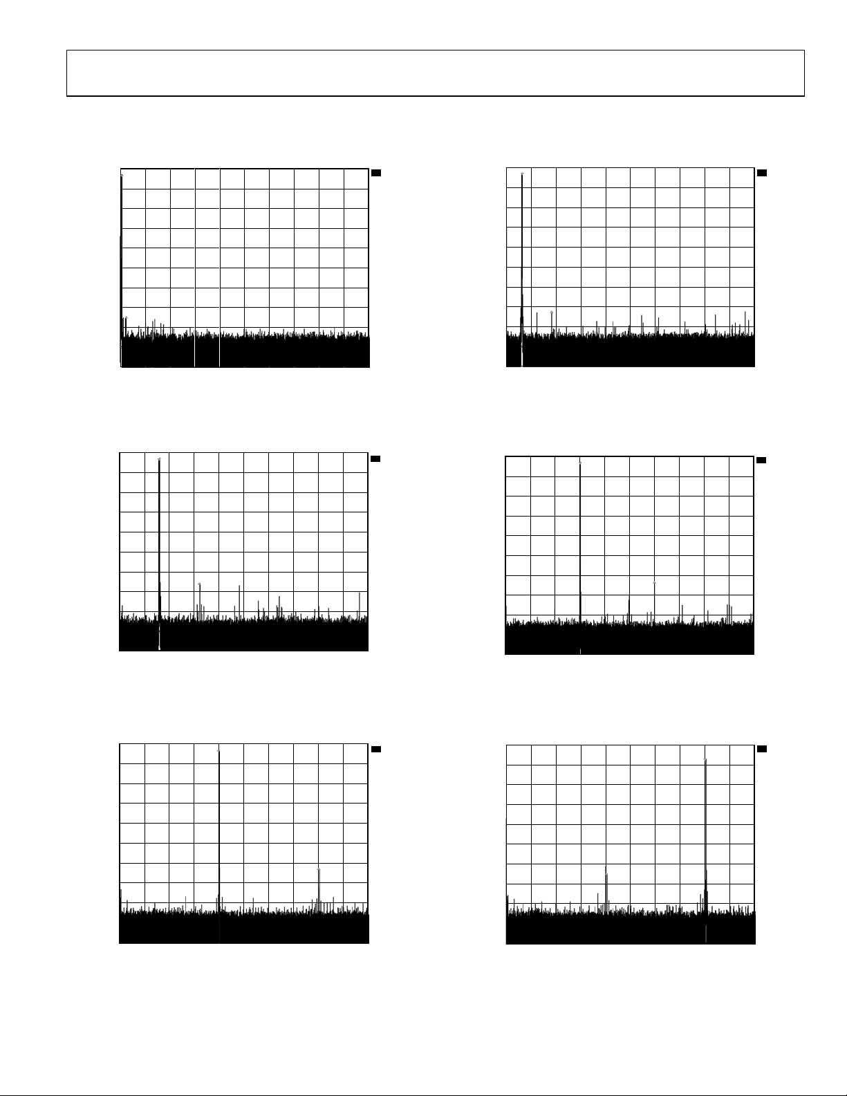
TYPICAL PERFORMANCE CHARACTERISTICS
Figure 4. Wideband SFDR, f
Figure 5. Wideband SFDR, f
= 1.1 MHz, f
OUT
= 40.1 MHz, f
OUT
= 500 MSPS
CLK
= 500 MSPS
CLK
Figure 7. Wideband SFDR, f
Figure 8. Wideband SFDR, f
= 15.1 MHz, f
OUT
= 75.1 MHz, f
OUT
= 500 MSPS
CLK
= 500 MSPS
CLK
Figure 6. Wideband SFDR, f
= 100.3 MHz, f
OUT
= 500 MSPS
CLK
Figure 9. Wideband SFDR, f
= 200.3 MHz, f
OUT
= 500 MSPS
CLK
Rev. C | Page 11 of 44
Page 12
AD9958 Data Sheet
0
–100
(dB)
–10
–20
–30
–40
–50
–60
–70
–80
–90
CENTER 1.1MHz
SPAN 1MHz
100kHz/DIV
DELTA 1 (T1)
–84.73dB
254.50901604kHz
RBW
500Hz
RF ATT 20dB
VBW 500Hz
SWT
20s
UNIT
dB
REF LVL
0dBm
A
1AP
1
05252-012
0
–100
(dB)
–10
–20
–30
–40
–50
–60
–70
–80
–90
CENTER 40.1MHz
SPAN 1MHz100kHz/DIV
DELTA 1 (T1)
–84.10dB
120.24048096kHz
RBW 500Hz
RF ATT
20dB
VBW
500Hz
SWT
20s UNIT
dB
REF LVL
0dBm
A
1AP
1
05252-013
0
–100
(dB)
–10
–20
–30
–40
–50
–60
–70
–80
–90
CENTER 100.3MHz
SPAN 1MHz100kHz/DIV
DELTA 1 (T 1)
–82.63dB
400.80160321kHz
RBW 500Hz RF ATT 20dB
VBW 500Hz
SWT 20s UNIT
dB
REF LVL
0dBm
A
1AP
1
05252-014
0
–100
(dB)
–10
–20
–30
–40
–50
–60
–70
–80
–90
CENTER 15.1MHz
SPAN 1MHz100kHz/DIV
DELTA 1 (T1)
–84.86dB
–200.40080160kHz
RBW
500Hz
RF ATT
20dB
VBW
500Hz
SWT 20s
UNIT
dB
REF LVL
0dBm
A
1AP
1
05252-015
0
–100
(dB)
–10
–20
–30
–40
–50
–60
–70
–80
–90
CENTER 75.1MHz
SPAN 1MHz100kHz/DIV
DELTA 1 (T1)
–86.03dB
262.56513026kHz
RBW
500Hz RF AT T
20dB
VBW
500Hz
SWT 20s
UNIT dB
REF LVL
0dBm
A
1AP
1
05252-016
0
–100
(dB)
–10
–20
–30
–40
–50
–60
–70
–80
–90
CENTER 200.3MHz
SPAN 1MHz100kHz/DIV
DELTA 1 (T1)
–83.72dB
–400.80160321kHz
RBW 500Hz
RF ATT 20dB
VBW 500Hz
SWT 20s UNIT dB
REF LVL
0dBm
A
1AP
1
05252-017
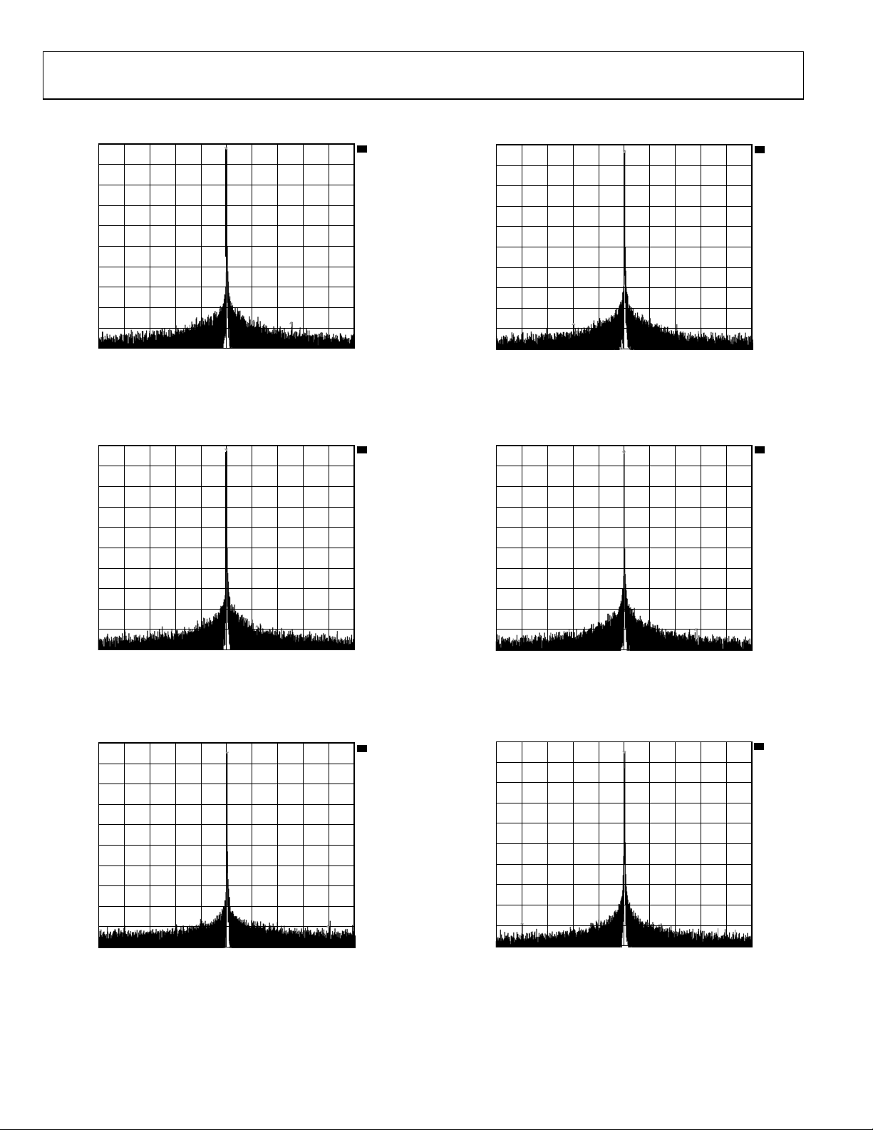
Figure 10. NBSFDR, f
Figure 11. NBSFDR, f
= 1.1 MHz, f
OUT
= 40.1 MHz, f
OUT
= 500 MSPS, ±1 MHz
CLK
= 500 MSPS, ±1 MHz
CLK
Figure 13. NBSFDR, f
Figure 14. NBSFDR, f
= 15.1 MHz, f
OUT
= 75.1 MHz, f
OUT
= 500 MSPS, ±1 MHz
CLK
= 500 MSPS, ±1 MHz
CLK
Figure 12. NBSFDR, f
OUT
= 100.3 MHz, f
CLK
= 500 MSPS, ±1 MHz
Rev. C | Page 12 of 44
Figure 15. NBSFDR f
= 200. 3MHz, f
OUT
= 500 MSPS, , ±1 MHz
CLK
Page 13
Data Sheet AD9958
–170
–160
–150
–140
–130
–120
–110
–100
10 100 1k 10k 100k 1M 10M
FREQUENCY OFFSET (Hz)
PHASE NOISE (dBc/Hz)
75.1MHz
100.3MHz
40.1MHz
15.1MHz
05252-018
–70
–170
10
10M
FREQUENCY OFFSET (Hz)
PHASE NOISE (dBc/Hz)
–80
–90
–100
–110
–120
–130
–140
–150
–160
100 1k 10k 100k 1M
100.3MHz
75.1MHz
15.1MHz
40.1MHz
05252-019
–70
–170
10
10M
FREQUENCY OFFSET (Hz)
PHASE NOISE (dBc/Hz)
–80
–90
–100
–110
–120
–130
–140
–150
–160
100 1k 10k 100k 1M
100.3MHz
75.1MHz
15.1MHz
40.1MHz
05252-020
–60
–85
25.3
200.3
–65
–70
–75
–80
50.3 75.3 100.3 125.3 150.3 175.3
SEPARATED DAC PO WER PLANES
SINGLE DAC P OWER PLANE
FREQUENCY O F COUPLING SPUR (MHz)
CHANNEL ISOLATION ( dBc)
05252-021
600
0
500
REFERENCE CLOCK FREQUENCY ( M Hz )
TOTAL POWER DISSIPATION (mW)
500
400
300
200
100
450 400 350 300 250 200
150 100
50
2 CHANNELS ON
1 CHANNEL ON
05252-022
–45
–75
1.1
f
OUT
(MHz)
SFDR (dBc)
–50
–55
–60
–65
–70
15.1 40.1 75.1 100.3 200.3
SFDR AVERAGED
05252-023
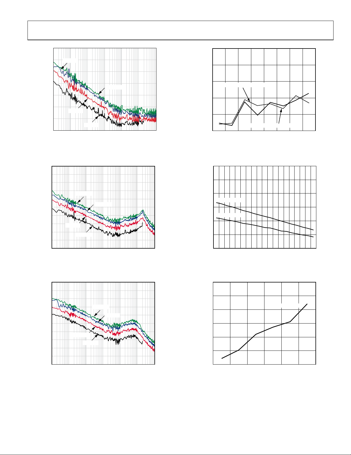
Figure 16. Residual Phase Noise (SSB) with f
75.1 MHz, 100.3 MHz; f
= 500 MHz with REFCLK Multiplier Bypassed
CLK
= 15.1 MHz, 40.1MHz,
OUT
Figure 19. Channel Isolation at 500 MSPS Operation; Conditions are Channel
of Interest Fixed at 110.3 MHz, the Other Channels Are Frequency Swept
Figure 17. Residual Phase Noise (SSB) with f
75.1 MHz, 100.3 MHz; f
Figure 18. Residual Phase Noise (SSB) with f
75.1 MHz,100.3 MHz; f
= 500 MHz with REFCLK Multiplier = 5×
CLK
= 500 MHz with REFCLK Multiplier = 20×
CLK
= 15.1 MHz, 40.1MHz,
OUT
= 15.1 MHz, 40.1MHz,
OUT
Figure 20. Power Dissipation vs. Reference Clock Frequency vs. Channel(s)
Power On/Off
Figure 21. Averaged Channel SFDR vs. f
OUT
Rev. C | Page 13 of 44
Page 14
AD9958 Data Sheet
A
APPLICATION CIRCUITS
PULSE
AD9958
CH0
FILTER
FILTER
ANTENNA
RADIATING
ELEMENTS
CH1
REFCLK
FILTER
LO
FILTER
05252-024
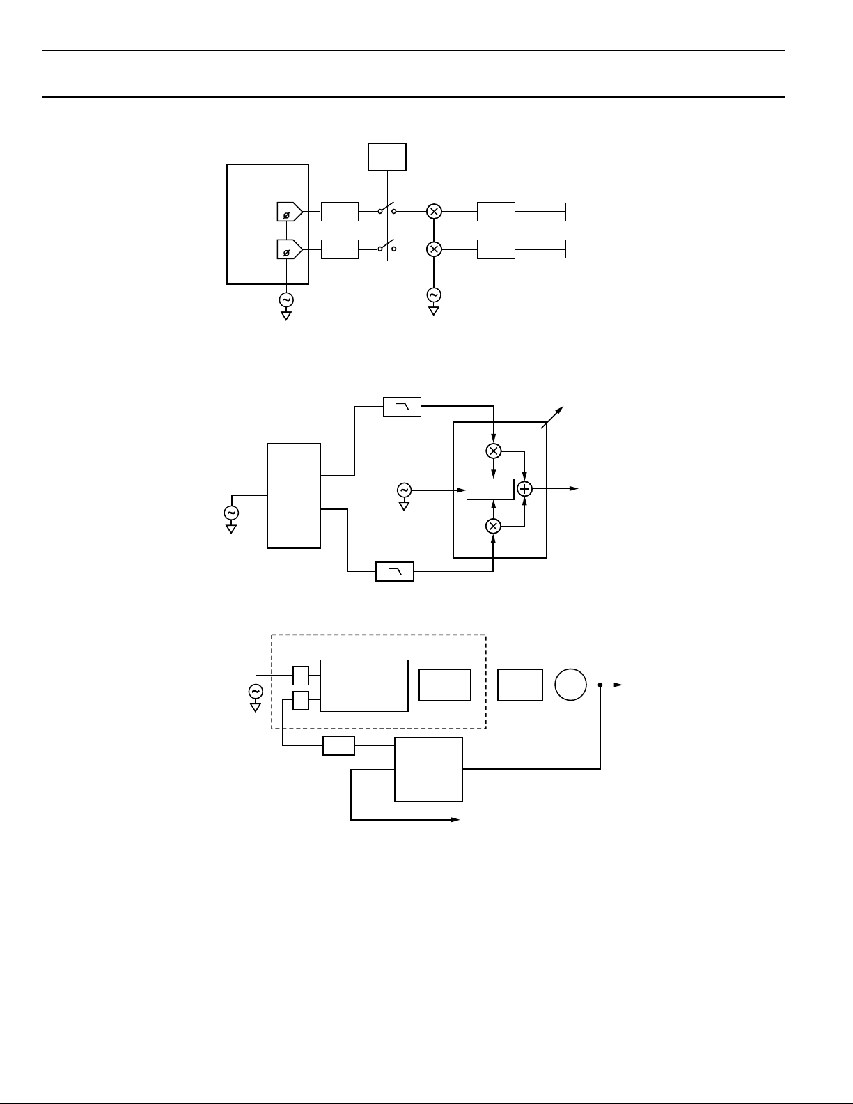
Figure 22. Phase Array Radar Using Precision Frequency/Phase Control from DDS in FMCW or Pulsed Radar Applications;
DDS Provides Either Continuous Wave or Frequency Sweep
D8348
I BASEBAND
AD8347
AD8346
ADL5390
AD8349
REFCLK
AD9958
CH0
CH1
LO
Q BASEBAND
PHASE
SPLITTER
RF OUTPUT
05252-025
Figure 23. Single-Sideband-Suppressed Carrier Upconversion
AD9510, AD9511, ADF4106
REFERENCE
÷
÷
PHASE
COMPARATOR
LPF
CHARGE
PUMP
AD9958
REFCLK
LOOP
FILTER
VCO
05252-026
Figure 24. DDS in PLL Locking to Reference Offering Distribution with Fine Frequency and Delay Adjust Tuning
Rev. C | Page 14 of 44
Page 15
Data Sheet AD9958
AD9510
CLOCK
SOURCE
CLOCK DISTRIBUTOR
WITH
DELAY EQUALI ZATION
REF_CLK
C1
S1
C2
S2
C3
S3
C4
S4
SYNC_OUT
AD9958
(MASTER)
AD9958
(SLAVE 1)
AD9958
(SLAVE 2)
AD9958
(SLAVE 3)
A1
A2
A3
A4
A_END
05252-027
CENTRAL
CONTROL
AD9510
SYNCHRONIZATION
DELAY EQUALIZATIO N
DATA
FPGA
SYNC_CLK
DATA
FPGA
SYNC_CLK
DATA
FPGA
SYNC_CLK
DATA
FPGA
SYNC_CLK
SYNC_IN
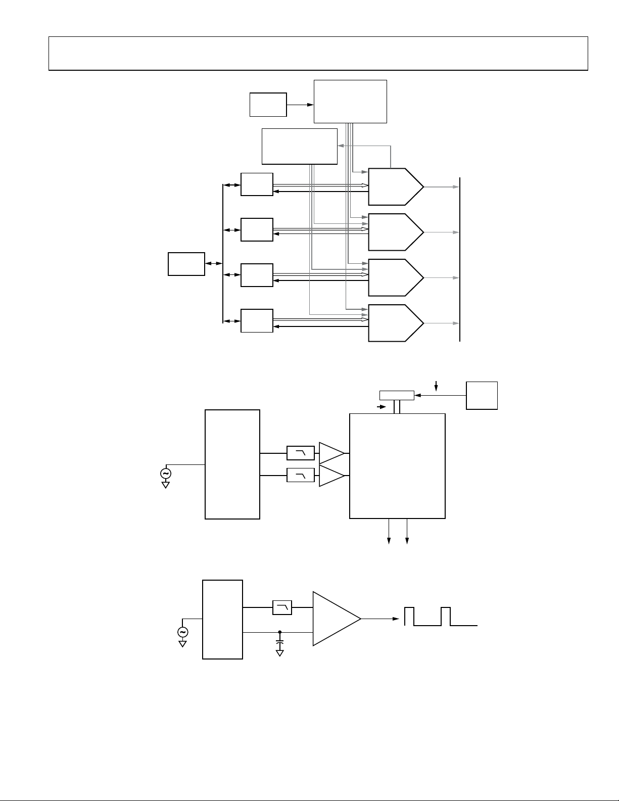
Figure 25. Synchronizing Multiple Devices to Increase Channel Capacity Using the AD9510 as a Clock Distributor for the Reference and SYNC_CLK
OPTICAL F IBER CHANNEL
WITH MULTIPLE DISCRETE
WAVELENGTHS
SPLITTER
WDM SIG NAL
INPUTS
WDM
SOURCE
REFCLK
AD9958
CH0
CH1
CH0
AMP
AMP
SELECTABLE WAVELENGTH FROM EACH
ACOUSTIC OPTICAL
TUNABLE FILTER
CH1
OUTPUTS
CH0 CH1
CHANNEL VIA DDS TUNI NG AOTF
05252-028
Figure 26. DDS Providing Stimulus for Acoustic Optical Tunable Filter
REFCLK
AD9958
CH0
CH1
–
ADCMP563
+
05252-029
Figure 27. Agile Clock Source with Duty Cycle Control Using the Phase Offset Value in DDS to Change the DC Voltage to the Comparator
Rev. C | Page 15 of 44
Page 16
AD9958 Data Sheet
CH0
CH1
AD9958
REFCLK
AD9515
AD9514
AD9513
AD9512
LVPECL
LVDS
CMOS
LVPECL
LVDS
CMOS
n
IMAGE
n
PROGRAMMABLE 1 TO 32
DIVIDER AND DEL AY ADJUS T
CLOCK OUTP UT
SELECTION(S)
n = DEPENDENT ON
PRODUCT SELECTION
AD9515
AD9514
AD9513
AD9512
05252-030
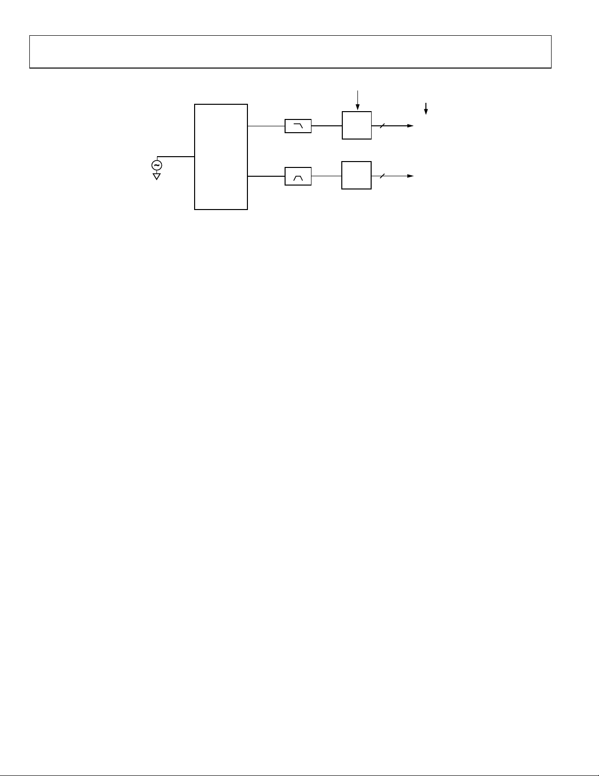
Figure 28. Clock Generation Circuit Using the AD9512/AD9513/AD9514/AD9515 Series of Clock Distribution Chips
Rev. C | Page 16 of 44
Page 17
Data Sheet AD9958
A
EQUIVALENT INPUT AND OUTPUT CIRCUITS
DVDD_I/O = 3. 3V
INPUT OUTPUT
AVOID OVERDRIVING
DIGITAL INPUTS.
FORWARD BIASING
DIODES MAY COUPLE
DIGITAL NOISE ON
POWER PINS.
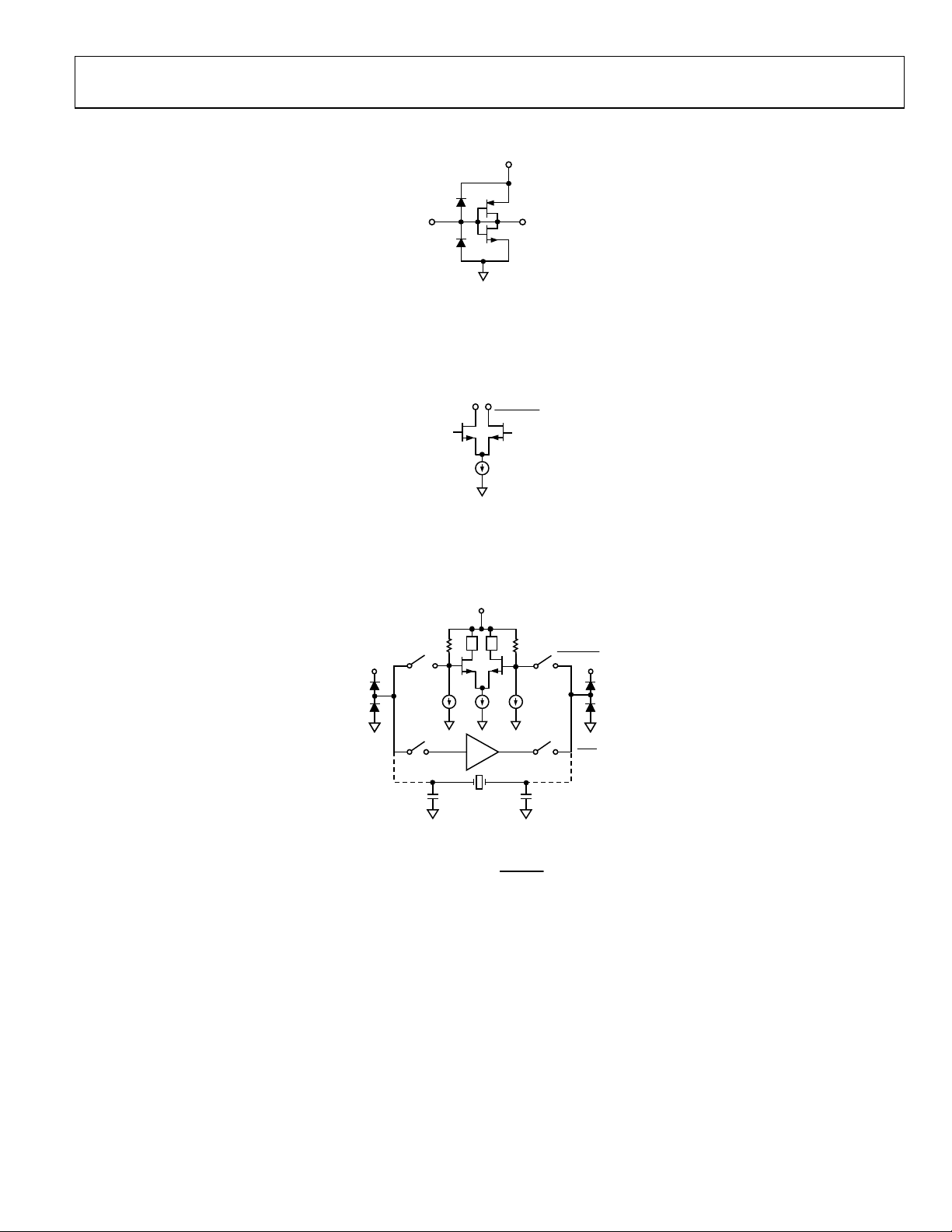
Figure 29. CMOS Digital Inputs
CHx_IOUT
TERMINATE OUTPUTS
INTO AVDD. DO NOT
EXCEED VOLTAGE
Figure 30. DAC Outputs
CHx_IOUT
COMPLIANCE O F
OUTPUTS.
VDD
05252-102
05252-132
REF_CLK REF_CLK
AVDD
1.5kΩ
NEED TO BE AC-CO UPLED.
OSC INPUTS ARE DC-CO UPLED.
Z Z
AMP
REF_CLK INPUTS ARE
INTERNALLY BIASED AND
Figure 31. REF_CLK/
1.5kΩ
REF_CLK
Inputs
AVDD
OSCOSC
05252-133
Rev. C | Page 17 of 44
Page 18

AD9958 Data Sheet
32
2
))((
S
OUT
fFTW
f =
°×
=
Φ 360
2
14
POW
(max)
91.18
OUT
SET
I
R =
DAC
LPF
CHx_IOUT
AVDD
1:1
50Ω
CHx_IOUT
05252-116
THEORY OF OPERATION
DDS CORE
The AD9958 has two DDS cores, each consisting of a 32-bit
phase accumulator and phase-to-amplitude converter. Together,
these digital blocks generate a digital sine wave when the phase
accumulator is clocked and the phase increment value (frequency
tuning word) is greater than 0. The phase-to-amplitude converter
simultaneously translates phase information to amplitude
information by a cos(θ) operation.
The output frequency (f
of the rollover rate of each phase accumulator. The exact
relationship is given in the following equation:
where:
f
is the system clock rate.
S
FTW is the frequency tuning word and is 0 ≤ FTW ≤ 2
32
2
represents the phase accumulator capacity.
Because both channels share a common system clock, they are
inherently synchronized.
The DDS core architecture also supports the capability to phase
offset the output signal, which is performed by the channel
phase offset word (CPOW). The CPOW is a 14-bit register that
stores a phase offset value. This value is added to the output of
the phase accumulator to offset the current phase of the output
signal. Each channel has its own phase offset word register. This
feature can be used for placing all channels in a known phase
relationship relative to one another. The exact value of phase
offset is given by the following equation:
) of each DDS channel is a function
OUT
31
.
DIGITAL-TO-ANALOG CONVERTER
The AD9958 incorporates four 10-bit current output DACs.
The DAC converts a digital code (amplitude) into a discrete
analog quantity. The DAC current outputs can be modeled as a
current source with high output impedance (typically 100 kΩ).
Unlike many DACs, these current outputs require termination
into AVDD via a resistor or a center-tapped transformer for
expected current flow.
Each DAC has complementary outputs that provide a combined
full-scale output current (I
current, and their sum equals the full-scale current at any point
in time. The full-scale current is controlled by means of an
external resistor (R
) and the scalable DAC current control
SET
bits discussed in the Modes of Operation section. The resistor,
R
, is connected between the DAC_RSET pin and analog
SET
ground (AGND). The full-scale current is inversely proportional
to the resistor value as follows:
The maximum full-scale output current of the combined DAC
outputs is 15 mA, but limiting the output to 10 mA provides
optimal spurious-free dynamic range (SFDR) performance.
The DAC output voltage compliance range is AVDD + 0.5 V to
AVDD − 0.5 V. Voltages developed beyond this range may cause
excessive harmonic distortion. Proper attention should be paid
to the load termination to keep the output voltage within its
compliance range. Exceeding this range could potentially damage the DAC output circuitry.
+ I
OUT
). The outputs always sink
OUT
Figure 32. Typical DAC Output Termination Configuration
Rev. C | Page 18 of 44
Page 19

Data Sheet AD9958
MODES OF OPERATION
There are many combinations of modes (for example, singletone, modulation, linear sweep) that the AD9958 can perform
simultaneously. However, some modes require multiple data
pins, which can impose limitations. The following guidelines
can help determine if a specific combination of modes can be
performed simultaneously by the AD9958.
CHANNEL CONSTRAINT GUIDELINES
• Single-tone mode, two-level modulation mode, and linear
sweep mode can be enabled on either channel and in any
combination simultaneously.
• Both channels can perform four-level modulation
simultaneously.
• Either channel can perform eight-level or 16-level
modulation. The other channel can only be in single-tone
mode.
• The RU/RD function can be used on both channels in
single-tone mode. See the Output Amplitude Control
Mode section for the RU/RD function.
• When Profile Pin P2 and Profile Pin P3 are used for
RU/RD, either channel can perform two-level modulation
with RU/RD or both channels can perform linear
frequency or phase sweep with RU/RD.
• When Profile Pin P3 is used for RU/RD, either channel can
be used in eight-level modulation with RU/RD. The other
channel can only be in single-tone mode.
• When SDIO_1, SDIO_2, and SDIO_3 pins are used for
RU/RD, either or both channels can perform two-level
modulation with RU/RD. If one channel is not in two-level
modulation, it can only be in single-tone mode.
• When the SDIO_1, SDIO_2, and SDIO_3 pins are used for
RU/RD, either or both channels can perform four-level
modulation with RU/RD. If one channel is not in four-level
modulation, it can only be in single-tone mode.
• When the SDIO_1, SDIO_2, and SDIO_3 pins are used for
RU/RD, either channel can perform eight-level modulation
with RU/RD. The other channel can only be in single-tone
mode.
• When the SDIO_1, SDIO_2, and SDIO_3 pins are used for
RU/RD, either channel can perform 16-level modulation with
RU/RD. The other channel can only be in single-tone mode.
• Amplitude modulation, linear amplitude sweep modes,
and the RU/RD function cannot operate simultaneously,
but frequency and phase modulation can operate
simultaneously with the RU/RD function.
POWER SUPPLIES
The AVDD and DVDD supply pins provide power to the DDS
core and supporting analog circuitry. These pins connect to a
1.8 V nominal power supply.
The DVDD_I/O pin connects to a 3.3 V nominal power supply.
All digital inputs are 3.3 V logic except for the CLK_MODE_SEL
input. CLK_MODE_SEL (Pin 24) is an analog input and should
be operated by 1.8 V logic.
SINGLE-TONE MODE
Single-tone mode is the default mode of operation after a master
reset signal. In this mode, both DDS channels share a common
address location for the frequency tuning word (Register 0x04)
and phase offset word (Register 0x05). Channel enable bits are
provided in combination with these shared addresses. As a
result, the frequency tuning word and/or phase offset word can
be independently programmed between channels (see the following Step 1 through Step 5). The channel enable bits do not
require an I/O update to enable or disable a channel.
See the Register Maps and Bit Descriptions section for a
description of the channel enable bits in the channel select
register (CSR, Register 0x00). The channel enable bits are
enabled or disabled immediately after the CSR data byte is
written.
Address sharing enables channels to be written simultaneously,
if desired. The default state enables all channel enable bits.
Therefore, the frequency tuning word and/or phase offset word
is common to all channels but written only once through the
serial I/O port.
The following steps present a basic protocol to program a
different frequency tuning word and/or phase offset word for
each channel using the channel enable bits.
1. Power up the DUT and issue a master reset. A master
reset places the part in single-tone mode and singlebit mode for serial programming operations (refer to the
Serial I/O Modes of Operation section). Frequency
tuning words and phase offset words default to 0 at
this point.
2. Enable only one channel enable bit (Register 0x00)
and disable the other channel enable bit.
3. Using the serial I/O port, program the desired
frequency tuning word (Register 0x04) and/or the
phase offset word (Register 0x05) for the enabled
channel.
4. Repeat Step 2 and Step 3 for each channel.
5. Send an I/O update signal. After an I/O update, all
channels should output their programmed frequency
and/or phase offset values.
Rev. C | Page 19 of 44
Page 20
AD9958 Data Sheet
CLK_MODE_SEL, Pin 24
FR1[22:18] PLL Divider Ratio = M
Crystal Oscillator E nabled
System Clock (f
)
Min/Max Freq. Range (MHz)
1:1
BALUN
REF_CLK
PIN 23
REFCLK
SOURCE
REF_CLK
PIN 22
50Ω
0.1µF
0.1µF
05252-117
REF_CLK
PIN 23
REF_CLK
PIN 22
0.1µF
0.1µF
LVPECL/
PECL
DRIVER
TERMINATION
05252-118
Single-Tone Mode—Matched Pipeline Delay
In single-tone mode, the AD9958 offers matched pipeline delay
to the DAC input for all frequency, phase, and amplitude changes.
This avoids having to deal with different pipeline delays between
the three input ports for such applications. The feature is enabled
by asserting the matched pipe delays active bit found in the
channel function register (CFR, Register 0x03). This feature
is available in single-tone mode only.
REFERENCE CLOCK MODES
The AD9958 supports multiple reference clock configurations
to generate the internal system clock. As an alternative to
clocking the part directly with a high frequency clock source,
the system clock can be generated using the internal, PLL-based
reference clock multiplier. An on-chip oscillator circuit is also
available for providing a low frequency reference signal by
connecting a crystal to the clock input pins. Enabling these
features allows the part to operate with a low frequency clock
source and still provide a high update rate for the DDS and
DAC. However, using the clock multiplier changes the output
phase noise characteristics. For best phase noise performance,
a clean, stable clock with a high slew is required (see Figure 17
and Figure 18).
Enabling the PLL allows multiplication of the reference clock
frequency from 4× to 20×, in integer steps. The PLL multiplication value is represented by a 5-bit multiplier value. These bits
are located in Function Register 1 (FR1, Register 0x01), Bits[22:18]
(see the Register Maps and Bit Descriptions section).
When FR1[22:18] is programmed with values ranging from
4 to 20 (decimal), the clock multiplier is enabled. The integer
value in the register represents the multiplication factor. The
system clock rate with the clock multiplier enabled is equal to
the reference clock rate multiplied by the multiplication factor.
If FR1[22:18] is programmed with a value less than 4 or greater
than 20, the clock multiplier is disabled and the multiplication
factor is effectively 1.
Whenever the PLL clock multiplier is enabled or the multiplication value is changed, time should be allowed to lock the PLL
(typically 1 ms).
Note that the output frequency of the PLL is restricted to a
frequency range of 100 MHz to 500 MHz. However, there is a
VCO gain control bit that must be used appropriately. The VCO
gain control bit defines two ranges (low/high) of frequency
output. The VCO gain control bit defaults to low (see Ta b l e 1
for details).
The charge pump current in the PLL defaults to 75 µA. This
setting typically produces the best phase noise characteristics.
Increasing the charge pump current may degrade phase noise,
but it decreases the lock time and changes the loop bandwidth.
Enabling the on-chip oscillator for crystal operation is performed
by driving CLK_MODE_SEL (Pin 24) to logic high (1.8 V
logic). With the on-chip oscillator enabled, connection of an
external crystal to the REF_CLK and
REF_CLK
inputs is made,
producing a low frequency reference clock. The frequency of
the crystal must be in the range of 20 MHz to 30 MHz.
Tabl e 4 summarizes the clock modes of operation. See Table 1
for more details.
Reference Clock Input Circuitry
The reference clock input circuitry has two modes of operation
controlled by the logic state of Pin 24 (CLK_MODE_SEL). The
first mode (logic low) configures as an input buffer. In this
mode, the reference clock must be ac-coupled to the input due
to internal dc biasing. This mode supports either differential
or single-ended configurations. If single-ended mode is chosen,
the complementary reference clock input (Pin 22) should be
decoupled to AVDD or AGND via a 0.1 µF capacitor. Figure 33
to Figure 35 exemplify typical reference clock configurations for
the AD9958.
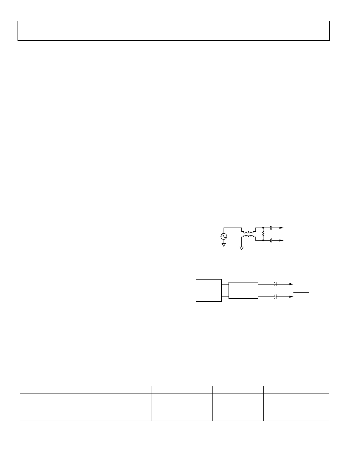
Figure 33. Differential Coupling from Single-Ended Source
The reference clock inputs can also support an LVPECL or
PECL driver as the reference clock source.
Figure 34. Differential Clock Source Hook-Up
The second mode of operation (Pin 24 = logic high = 1.8 V)
provides an internal oscillator for crystal operation. In this
mode, both clock inputs are dc-coupled via the crystal leads
and are bypassed. The range of crystal frequencies supported is
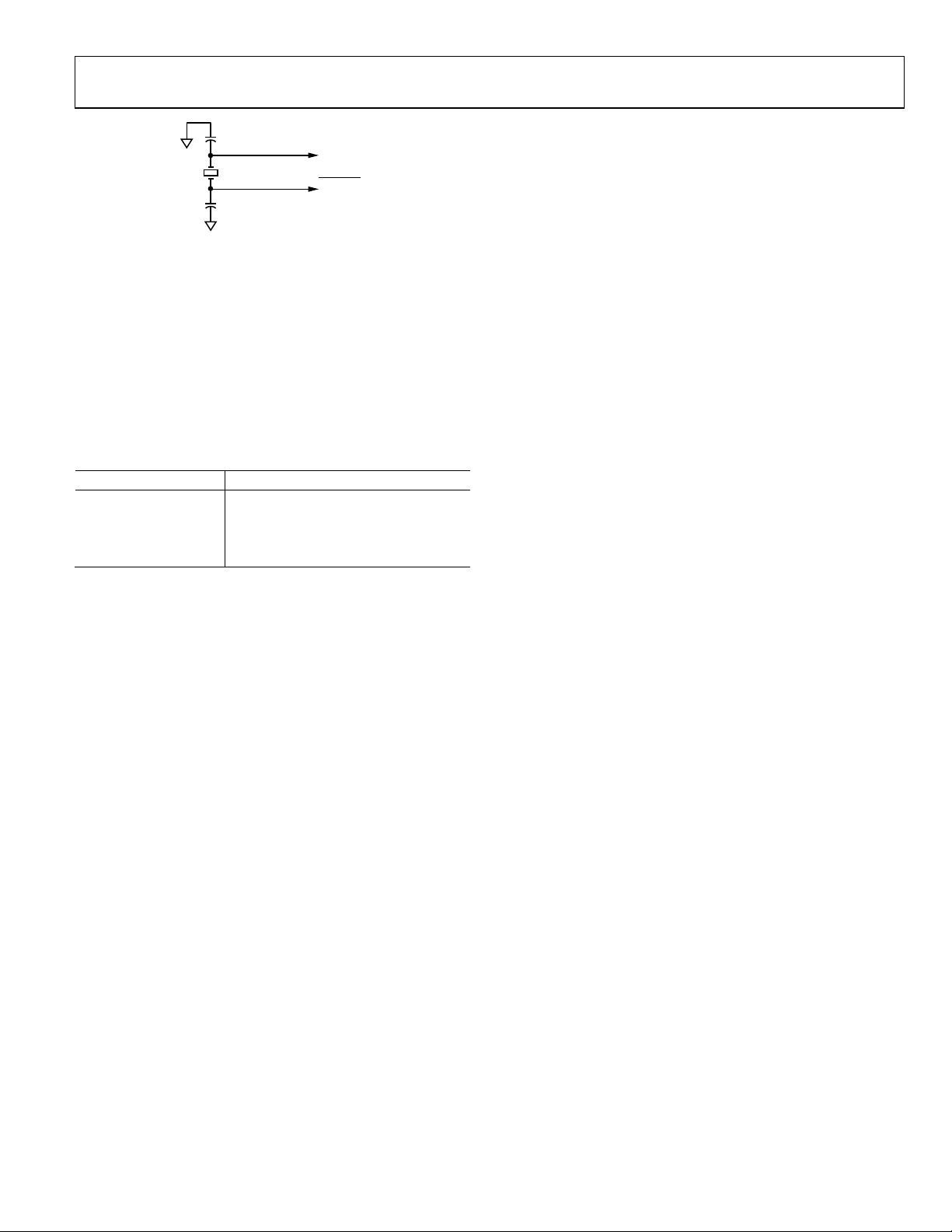
from 20 MHz to 30 MHz. Figure 35 shows the configuration
for using a crystal.
Table 4. Clock Configuration
High = 1.8 V Logic 4 ≤ M ≤ 20 Yes f
High = 1.8 V Logic M < 4 or M > 20 Yes f
Low 4 ≤ M ≤ 20 No f
Low M < 4 or M > 20 No f
SYSCLK
= f
SYSCLK
SYSCLK
SYSCLK
SYSCLK
Rev. C | Page 20 of 44
× M 100 < f
OSC
= f
20 < f
OSC
= f
× M 100 < f
REFCLK
= f
0 < f
REFCLK
SYSCLK
SYSCLK
SYSCLK
SYSCLK
< 500
< 500
< 30
< 500
Page 21
Data Sheet AD9958
REF_CLK
PIN 23
25MHz
XTAL
REF_CLK
PIN 22
39pF
39pF
05252-119
When FR1[6] = 1 and the PWR_DWN_CTL input pin is high,
the AD9958 is put into full power-down mode. In this mode, all
functions are powered down. This includes the DAC and PLL,
which take a significant amount of time to power up. When the
PLL is bypassed, the PLL is shut down to conserve power.
Figure 35. Crystal Input Configuration
SCALABLE DAC REFERENCE CURRENT CONTROL MODE
R
is common to all four DACs. As a result, the full-scale
SET
currents are equal by default. The scalable DAC reference can
be used to set the full-scale current of each DAC independent
from one another. This is accomplished by using the register
bits CFR[9:8]. Table 5 shows how each DAC can be individually
scaled for independent channel control. This scaling provides
for binary attenuation.
Table 5. DAC Full-Scale Current Control
CFR[9:8] LSB Current State
11 Full scale
01 Half scale
10 Quarter scale
00 Eighth scale
POWER-DOWN FUNCTIONS
The AD9958 supports an externally controlled power-down
feature and the more common software programmable powerdown bits found in previous Analog Devices DDS products.
The software control power-down allows the input clock circuitry, the DAC, and the digital logic (for each separate channel) to
be individually powered down via unique control bits (CFR[7:6]).
These bits are not active when the externally controlled powerdown pin (PWR_DWN_CTL) is high. When the input pin,
PWR_DWN_CTL, is high, the AD9958 enters a power-down
mode based on the FR1[6] bit. When the PWR_DWN_CTL
input pin is low, the external power-down control is inactive.
When FR1[6] = 0 and the PWR_DWN_CTL input pin is high,
the AD9958 is put into a fast recovery power-down mode. In
this mode, the digital logic and the DAC digital logic are powered
down. The DAC bias circuitry, PLL, oscillator, and clock input
circuitry are not powered down.
When the PWR_DWN_CTL input pin is high, the individual
power-down bits (CFR[7:6]) and (FR1[7]) are invalid (don’t
care) and unused. When the PWR_DWN_CTL input pin is low,
the individual power-down bits control the power-down modes
of operation.
Note that the power-down signals are all designed such that
Logic 1 indicates the low power mode and Logic 0 indicates the
powered-up mode.
MODULATION MODE
The AD9958 can perform 2-/4-/8-/16-level modulation of
frequency, phase, or amplitude. Modulation is achieved by
applying data to the profile pins. Each channel can be programmed separately, but the ability to modulate multiple channels
simultaneously is constrained by the limited number of profile
pins. For instance, 16-level modulation uses all four profile pins,
which inhibits modulation for the remaining channel.
In addition, the AD9958 has the ability to ramp up or ramp
down the output amplitude before, during, or after a modulation
(FSK, PSK only) sequence. This is performed by using the 10-bit
output scalar. If the RU/RD feature is desired, unused profile
pins or unused SDIO_1/SDIO_2/SDIO_3 pins can be configured to initiate the operation. See the Output Amplitude
Control Mode section for more details of the RU/RD feature.
In modulation mode, each channel has its own set of control
bits to determine the type (frequency, phase, or amplitude)
of modulation. Each channel has 16 profile (channel word)
registers for flexibility. Register 0x0A through Register 0x18
are profile registers for modulation of frequency, phase, or
amplitude. Register 0x04, Register 0x05, and Register 0x06
are dedicated registers for frequency, phase, and amplitude,
respectively. These registers contain the first frequency, phase
offset, and amplitude word.
Frequency modulation has 32-bit resolution, phase modulation is
14 bits, and amplitude is 10 bits. When modulating phase or
amplitude, the word value must be MSB aligned in the profile
(channel word) registers and the unused bits are don’t care bits.
Rev. C | Page 21 of 44
Page 22
AD9958 Data Sheet
Modulation Level (FR1[9:8])
Description
In modulation mode, the amplitude frequency phase (AFP)
select bits (CFR[23:22]) and modulation level bits (FR1[9:8])
are programmed to configure the modulation type and level
(see Table 6 and Ta bl e 7). Note that the linear sweep enable bit
must be set to Logic 0 in direct modulation mode.
Table 6. Modulation Type Configuration
AFP Select
(CFR[23:22])
00 X Modulation disabled
01 0 Amplitude modulation
10 0 Frequency modulation
11 0 Phase modulation
Linear Sweep Enable
(CFR[14]) Description
Table 7. Modulation Level Selection
00 Two-level modulation
01 Four-level modulation
10 Eight-level modulation
11 16-level modulation
When modulating, the RU/RD function can be limited based
on pins available for controlling the feature. The SDIO_x pins
are for RU/RD only, not for modulation.
Table 8. RU/RD Profile Pin Assignments
Ramp-Up/Ramp-Down
(RU/RD) (FR1[11:10]) Description
00 RU/RD disabled
01 Only Profile Pin P2 and Profile Pin P3
available for RU/RD operation
10 Only Profile Pin P3 available for RU/RD
operation
11 Only SDIO_1, SDIO_2, and SDIO_3
pins available for RU/RD operation;
this forces the serial I/O to be used
only in 1-bit mode
If the profile pins are used for RU/RD, Logic 0 is for ramp-up
and Logic 1 is for ramp-down.
Because of the two channels and limited data pins, it is
necessary to assign the profile pins and/or SDIO_1, SDIO_2,
and SDIO_3 pins to a dedicated channel. This is controlled by
the profile pin configuration (PPC) bits (FR1[14:12]). Each of the
following modulation descriptions incorporates data pin
assignments.
Two-Level Modulation—No RU/RD
The modulation level bits (FR1[9:8]) are set to 00 (two-level).
The AFP select bits (CFR[23:22]) are set to the desired modulation
type. The RU/RD bits (FR1[11:10]) and the linear sweep enable
bit (CFR[14]) are disabled. Tab l e 9 displays how the profile pins
and channels are assigned.
As shown in Tabl e 9, only Profile Pin P2 can be used to modulate
Channel 0. If frequency modulation is selected and Profile Pin P2
is Logic 0, Channel Frequency Tuning Word 0 (Register 0x04) is
chosen; if Profile Pin P2 is Logic 1, Channel Word 1 (Register
0x0A) is chosen.
Four-Level Modulation—No RU/RD
The modulation level bits are set to 01 (four-level). The AFP
select bits (CFR[23:22]) are set to the desired modulation type.
The RU/RD bits (FR1[11:10]) and the linear sweep enable bit
(CFR[14]) are disabled. Table 10 displays how the profile pins
and channels are assigned to each other.
For the conditions in Tabl e 10, the profile (channel word)
register chosen is based on the 2-bit value presented to Profile
Pins [P0:P1] or Profile Pins [P2:P3].
For example, if PPC = 101, [P0:P1] = 11, and [P2:P3] = 01, then
the contents of the Channel Word 3 register of Channel 0 are
presented to the output of Channel 0 and the contents of the
Channel Word 1 register of Channel 1 are presented to the
output of Channel 1.
Table 9. Profile Pin Channel Assignments
Profile Pin Configuration (PPC) (FR1[14:12]) P0 P1 P2 P3 Description
XXX N/A N/A CH0 CH1 Two-level modulation, both channels, no RU/RD
Table 10. Profile Pin and Channel Assignments
Profile Pin Configuration (PPC) (FR1[14:12]) P0 P1 P2 P3 Description
101 CH0 CH0 CH1 CH1 Four-level modulation on CH0 and CH1, no RU/RD
Rev. C | Page 22 of 44
Page 23

Data Sheet AD9958
Eight-Level Modulation—No RU/RD
The modulation level bits (FR1[9:8]) are set to 10 (eight-level).
The AFP select bits (CFR[23:22]) are set to a nonzero value.
The RU/RD bits (FR1[11:10]) and the linear sweep enable bit
(CFR[14]) are disabled. Note that the AFP select bits of the
other channel not being used must be set to 00. Table 11 shows
the assignment of profile pins and channels.
For the condition in Tabl e 11, the choice of channel word registers
is based on the 3-bit value presented to Profile Pins [P0:P2]. For
example, if PPC = X10 and [P0:P2] = 111, the contents of the
Channel Word 7 register of Channel 0 are presented to the output
Channel 0.
16-Level Modulation—No RU/RD
The modulation level bits (FR1[9:8]) are set to 11 (16-level).
The AFP select bits (CFR[23:22]) are set to the desired modulation
type. The RU/RD bits (FR1[11:10]) and the linear sweep enable
bit (CFR[14]) are disabled. The AFP select bits of the other channel
not being used must be set to 00. Tabl e 12 displays how the profile
pins and channels are assigned.
Table 11. Profile Pin and Channel Assignments for Eight-Level Modulation (No RU/RD)
Profile Pin Config. (PPC)
(FR1[14:12]) P0 P1 P2 P3 Description
X10 CH0 CH0 CH0 X Eight-level modulation on CH0, no RU/RD
X11 CH1 CH1 CH1 X Eight-level modulation on CH1, no RU/RD
For the conditions in Ta bl e 12, the profile register chosen is
based on the 4-bit value presented to Profile Pins [P0:P3]. For
example, if PPC = X11 and [P0:P3] = 1110, the contents of the
Channel Word 14 register of Channel 1 is presented to the
output of Channel 1.
Two-Level Modulation Using Profile Pins for RU/RD
When the RU/RD bits = 01, Profile Pin P2 and Profile Pin P3
are available for RU/RD. Note that only a modulation level of
two is available in this mode. See Ta b l e 13 for available pin
assignments.
Eight-Level Modulation Using a Profile Pin for RU/RD
When the RU/RD bits = 10, Profile Pin P3 is available for
RU/RD. Note that only a modulation level of eight is available
in this mode. See Table 14 for available pin assignments.
Table 12. Profile Pin and Channel Assignments for 16-Level Modulation (No RU/RD)
Profile Pin Config. (PPC)
(FR1[14:12]) P0 P1 P2 P3 Description
X10 CH0 CH0 CH0 CH0 16-level modulation on CH0, no RU/RD
X11 CH1 CH1 CH1 CH1 16-level modulation on CH1, no RU/RD
Table 13. Profile Pin and Channel Assignments for Two-Level Modulation (RU/RD Enabled)
Profile Pin Config. (PPC)
(FR1[14:12]) P0 P1 P2 P3 Description
101 CH0 CH1 CH0 RU/RD CH1 RU/RD Two-level modulation on CH0 and CH1 with RU/RD
Table 14. Profile Pin and Channel Assignments for Eight-Level Modulation (RU/RD Enabled)
Profile Pin Config. (PPC)
(FR1[14:12]) P0 P1 P2 P3 Description
X10 CH0 CH0 CH0 CH0 RU/RD Eight-level modulation on CH0 with RU/RD
X11 CH1 CH1 CH1 CH1 RU/RD Eight-level modulation on CH1 with RU/RD
Rev. C | Page 23 of 44
Page 24
AD9958 Data Sheet
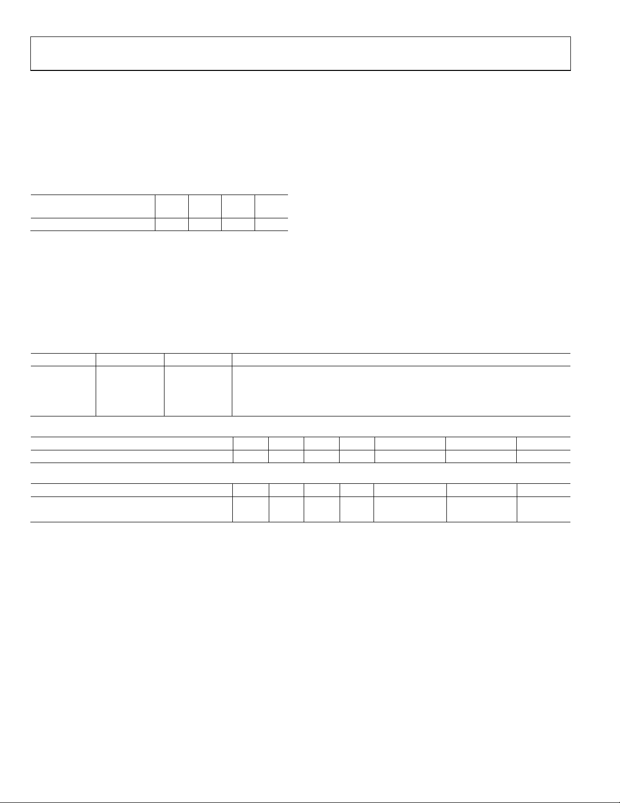
1 1 0
Triggers the ramp-up function for CH1
MODULATION USING SDIO_x PINS FOR RU/RD
For RU/RD bits = 11, the SDIO_1, SDIO_2, and SDIO_3 pins
are available for RU/RD. In this mode, modulation levels of 2, 4,
and 16 are available. Note that the serial I/O port can be used only
in 1-bit serial mode.
Two-Level Modulation Using SDIO Pins for RU/RD
Table 15. Profile Pin and Channel Assignments in Two-Level
Modulation (RU/RD Enabled)
Profile Pin Config. (PPC)
(FR1[14:12]) P0 P1 P2 P3
XXX N/A N/A CH0 CH1
For the configuration in Table 15, each profile pin is dedicated
to a specific channel. In this case, the SDIO_x pins can be used
for the RU/RD function, as described in Table 16.
Four-Level Modulation Using SDIO Pins for RU/RD
For RU/RD bits = 11 (the SDIO_1 and SDIO_2 pins are available for RU/RD), the modulation level is set to 4. See Table 17
for pin assignments, including SDIO_x pin assignments.
Table 16. Channel and SDIO_1/SDIO_2/SDIO_3 Pin Assignments for RU/RD Operation
SDIO_1 SDIO_2 SDIO_3 Description
1 0 0 Triggers the ramp-up function for CH0
1 0 1 Triggers the ramp-down function for CH0
For the configuration shown in Table 17, the profile (channel
word) register is chosen based on the 2-bit value presented to
Profile Pins [P1:P2] or [P3:P4].
For example, if PPC = 101, [P0:P1] = 11, and [P2:P3] = 01, the
contents of the Channel Word 3 register of Channel 0 are
presented to the output of Channel 0 and the contents of the
Channel Word 1 register of Channel 1 are presented to the
output of Channel 1. SDIO_1 and SDIO_2 provide the RU/RD
function.
16-Level Modulation Using SDIO Pins for RU/RD
The RU/RD bits = 11 (SDIO_1 available for RU/RD), and the
level is set to 16. See the pin assignments shown in Table 18.
For the configuration shown in Table 18, the profile (channel
word) register is chosen based on the 4-bit value presented to
Profile Pins [P0:P3]. For example, if PPC = X10 and [P0:P3] =
1101, then the contents of the Channel Word 13 register of
Channel 0 is presented to the output of Channel 0. The SDIO_1
pin provides the RU/RD function.
1 1 1 Triggers the ramp-down function for CH1
Table 17. Channel and Profile Pin Assignments, Including SDIO_1/SDIO_2/SDIO_3 Pin Assignments for RU/RD Operation
Profile Pin Configuration (PPC) (FR1[14:12]) P0 P1 P2 P3 SDIO_1 SDIO_2 SDIO_3
101 CH0 CH0 CH1 CH1 CH0 RU/RD CH1 RU/RD N/A
Table 18. Channel and Profile Pin Assignments, Including SDIO_1 Pin Assignments for RU/RD Operation
Profile Pin Configuration (PPC) (FR1[14:12]) P0 P1 P2 P3 SDIO_1 SDIO_2 SDIO_3
X10 CH0 CH0 CH0 CH0 CH0 RU/RD N/A N/A
X11 CH1 CH1 CH1 CH1 CH1 RU/RD N/A N/A
Rev. C | Page 24 of 44
Page 25
Data Sheet AD9958
LINEAR SWEEP MODE
Linear sweep mode enables the user to sweep frequency, phase,
or amplitude from a starting point (S0) to an endpoint (E0).
The purpose of linear sweep mode is to provide better bandwidth containment compared to direct modulation by replacing
greater instantaneous changes with more gradual, user-defined
changes between S0 and E0.
In linear sweep mode, S0 is loaded into the Channel Word 0
register (S0 is represented by one of three registers: Register 0x04,
Register 0x05, or Register 0x06, depending on the type of sweep)
and E0 is always loaded into Channel Word 1 (Register 0x0A).
If E0 is configured for frequency sweep, the resolution is 32 bits,
phase sweep is 14 bits, and amplitude sweep is 10 bits. When
sweeping phase or amplitude, the word value must be MSB aligned
in the Channel Word 1 register. The unused bits are don’t care
bits. The profile pins are used to trigger and control the direction
of the linear sweep for frequency, phase, and amplitude. All
channels can be programmed separately for a linear sweep. In
linear sweep mode, Profile Pin P2 is dedicated to Channel 0.
Profile Pin P3 is dedicated to Channel 1.
The AD9958 has the ability to ramp up or ramp down (RU/RD)
the output amplitude (using the 10-bit output scalar) before and
after a linear sweep. If the RU/RD feature is desired, unused
profile pins or unused SDIO_1/SDIO_2/SDIO_3 pins can be
configured for the RU/RD operation.
To enable linear sweep mode for a particular channel, the AFP
select bits (CFR[23:22]), the modulation level bits (FR1[9:8]),
and the linear sweep enable bit (CFR[14]) are programmed.
The AFP select bits determine the type of linear sweep to be
performed. The modulation level bits must be set to 00 (twolevel) for that specific channel (see Table 19 and Table 20)
Table 19. Linear Sweep Parameter to Sweep
AFP Select
(CFR[23:22])
00 1 N/A
01 1 Amplitude sweep
10 1 Frequency sweep
11 1 Phase sweep
Table 20. Modulation Level Assignments
Modulation Level (FR1[9:8]) Description
00 (Required in Linear Sweep) Two-level modulation
01 Four-level modulation
10 Eight-level modulation
11 16-level modulation
Linear Sweep Enable
(CFR[14]) Description
Setting the Slope of the Linear Sweep
The slope of the linear sweep is set by the intermediate step size
(delta-tuning word) between S0 and E0 and the time spent
(sweep ramp rate word) at each step. The resolution of the
delta-tuning word is 32 bits for frequency, 14 bits for phase, and
10 bits for amplitude. The resolution for the delta ramp rate
word is eight bits.
In linear sweep, each channel is assigned a rising delta word
(RDW, Register 0x08) and a rising sweep ramp rate word
(RSRR, Register 0x07). These settings apply when sweeping up
toward E0. The falling delta word (FDW, Register 0x09) and
falling sweep ramp rate (FSRR, Register 0x07) apply when
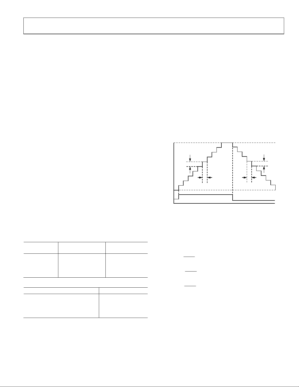
sweeping down toward S0. Figure 36 displays a linear sweep up
and then down using a profile pin. Note that the linear sweep
no-dwell bit is disabled; otherwise, the sweep accumulator
returns to 0 upon reaching E0.
E0
RDW
∆f,p,a
LINEAR SWEEP
(FREQUENCY/PHASE/AMPLI TUDE)
S0
PROFILE PIN
Figure 36. Linear Sweep Parameters
RSRR F SRR
∆t ∆t
TIME
FDW
∆f,p,a
For a piecemeal or a nonlinear transition between S0 and E0,
the delta-tuning words and ramp rate words can be reprogrammed during the transition to produce the desired response.
The formulas for calculating the step size of RDW or FDW for
delta frequency, delta phase, or delta amplitude are as follows:
RDW
f
32
2
RDW
ΔΦ
360
14
2
RDW
a
10
2
SYSCLK
1024
(Hz)
(DAC full-scale current)
The formula for calculating delta time from RSRR or FSRR is
CLKSYNCRSRRt _/1
At 500 MSPS operation (SYNC_CLK = 125 MHz), the maximum time interval between steps is 1/125 MHz × 256 = 2.048 μs.
The minimum time interval is (1/125 MHz) × 1 = 8.0 ns.
The sweep ramp rate block (timer) consists of a loadable 8-bit
down counter that continuously counts down from the loaded
value to 1. When the ramp rate timer equals 1, the proper ramp rate
value is loaded and the counter begins counting down to 1 again.
05252-120
Rev. C | Page 25 of 44
Page 26
AD9958 Data Sheet
R
This load and countdown operation continues for as long as the
timer is enabled. However, the count can be reloaded before
reaching 1 by either of the following two methods:
Method 1 is to change the profile pin. When the profile pin
changes from Logic 0 to Logic 1, the rising sweep ramp rate
(RSRR) register value is loaded into the ramp rate timer,
which then proceeds to count down as normal. When the
profile pin changes from Logic 1 to Logic 0, the falling sweep
ramp rate (FSRR) register value is loaded into the ramp
rate timer, which then proceeds to count down as normal.
Method 2 is to set the CFR[13] bit and issue an I/O update.
If linear sweep is enabled and CFR[13] is set, the ramp rate
timer loads the value determined by the profile pin. If the
profile pin is high, the ramp rate timer loads the RSRR; if the
profile pin is low, the ramp rate timer loads FSRR.
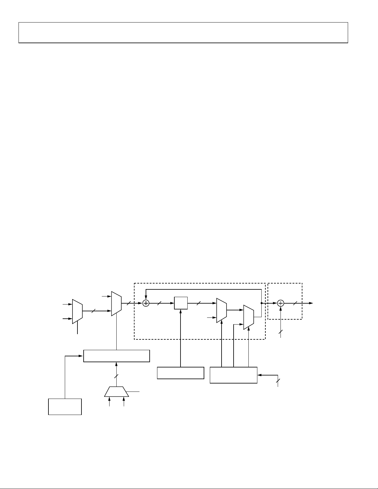
Frequency Linear Sweep Example: AFP Bits = 10
In the following example, the modulation level bits (FR1[9:8]) = 00,
the linear sweep enable bit (CFR[14]) = 1, and the linear sweep
no-dwell bit (CFR[15]) = 0.
In linear sweep mode, when the profile pin transitions from low
to high, the RDW is applied to the input of the sweep accumulator
and the RSRR register is loaded into the sweep rate timer.
The RDW accumulates at the rate given by the rising sweep
ramp rate (RSRR) bits until the output is equal to the CW1
register value. The sweep is then complete, and the output is
held constant in frequency.
When the profile pin transitions from high to low, the FDW is
applied to the input of the sweep accumulator and the FSRR bits
are loaded into the sweep rate timer.
The FDW accumulates at the rate given by the falling sweep ramp
rate (FSRR) until the output is equal to the CFTW0 register
(Register 0x04) value. The sweep is then complete, and the output
is held constant in frequency.
See Figure 37 for the linear sweep block diagram. Figure 39
depicts a frequency sweep with no-dwell mode disabled. In this
mode, the output follows the state of the profile pin. A phase or
amplitude sweep works in the same manner.
LINEAR SWEEP NO-DWELL MODE
If the linear sweep no-dwell bit is set (CFR[15]), the rising sweep is
started in an identical manner to the dwell linear sweep mode;
that is, upon detecting Logic 1 on the profile input pin, the rising
sweep action is initiated. The word continues to sweep up at the
rate set by the rising sweep ramp rate at the resolution set by the
rising delta word until it reaches the terminal value. Upon reaching
the terminal value, the output immediately reverts to the starting
point and remains until Logic 1 is detected on the profile pin.
Figure 38 shows an example of the no-dwell mode. The points
labeled A indicate where a rising edge is detected on the profile
pin, and the points labeled B indicate where the AD9958 has
determined that the output has reached E0 and reverts to S0.
The falling sweep ramp rate bits (LSRR[15:8]) and the falling
delta word bits (FDW[31:0]) are unused in this mode.
SWEEPACCUMULATOR SWEEP ADDE
FDW
RDW
RATE TIME
LOAD CONTROL
0
MUX
1
PROFILE PIN
LOGIC
0
0
32 32 32 32
32
8-BIT LOADABLE DOWN COUNTER
MUX
1
RAMP RATE TIMER:
8
MUX
1
0
FSRR RSRR
Figure 37. Linear Sweep Block Diagram (Frequency Sweep)
PROFILE PIN
–1
Z
ACCUMULATOR RESET
LOGIC
Rev. C | Page 26 of 44
0
MUX
1
0
LIMIT LOGIC TO
KEEP SWEEP BETWEEN
S0 AND E0
0
MUX
1
CFTW0
32
CW1
32
05252-121
Page 27
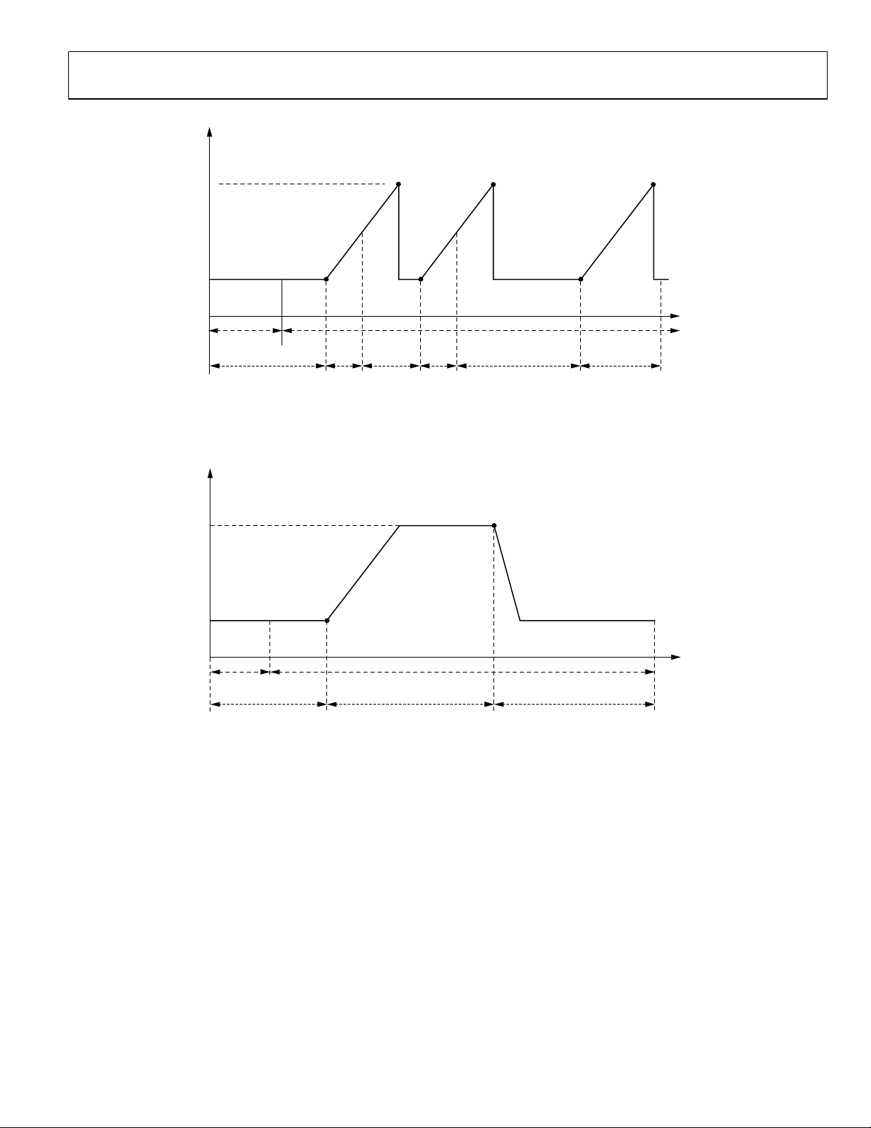
Data Sheet AD9958
f
OUT
FTW1
FTW0
SINGLE-TONE
MODE
AA A
P2 = 1 P2 = 0P2 = 0 P2 = 1 P2 = 1P2 = 0
LINEAR SWEEP MODE ENABLE—NO-DWELL BIT SET
BBB
TIME
05252-147
Figure 38. Channel 0 in Linear Sweep Mode (No-Dwell Enabled)
f
OUT
FTW1
B
FTW0
SINGLE-TONE
MODE
AT POINT A: LOAD RISI NG RAMP RATE REG ISTER, APPLY RDW<31:0>
AT POINT B: LOAD FALL ING RAMP RATE REGISTER, APPLY FDW <31:0>
A
LINEAR SWEE P MODE
P2 = 1P2 = 0 P2 = 0
Figure 39. Channel 0 in Linear Sweep Mode (No-Dwell Disabled)
SWEEP AND PHASE ACCUMULATOR CLEARING FUNCTIONS
The AD9958 allows two different clearing functions. The first
is a continuous zeroing of the sweep logic and phase accumulator (clear and hold). The second is a clear and release or automatic
zeroing function. CFR[4] is the autoclear sweep accumulator bit
and CFR[2] is the autoclear phase accumulator bit. The continuous
clear bits are located in CFR, where CFR[3] clears the sweep
accumulator and CFR[1] clears the phase accumulator.
TIME
05252-148
Continuous Clear Bits
The continuous clear bits are static control signals that, when
active high, hold the respective accumulator at 0 while the bit is
active. When the bit goes low, the respective accumulator is
allowed to operate.
Clear and Release Bits
The autoclear sweep accumulator bit, when set, clears and
releases the sweep accumulator upon an I/O update or a change
in the profile input pins. The autoclear phase accumulator bit,
when set, clears and releases the phase accumulator upon an
I/O update or a change in the profile pins. The automatic
clearing function is repeated for every subsequent I/O update or
change in profile pins until the clear and release bits are reset
via the serial port.
Rev. C | Page 27 of 44
Page 28

AD9958 Data Sheet
00
1
OUTPUT AMPLITUDE CONTROL MODE
The 10-bit scale factor (multiplier) controls the ramp-up and
ramp-down (RU/RD) time of an on/off emission from the DAC.
In burst transmissions of digital data, it reduces the adverse
spectral impact of abrupt bursts of data. The multiplier can
be bypassed by clearing the amplitude multiplier enable bit
(ACR[12] = 0).
Automatic and manual RU/RD modes are supported. The automatic mode generates a zero-scale up to a full-scale (10 bits)
linear ramp at a rate determined by ACR (Register 0x06). The
start and direction of the ramp can be controlled by either the
profile pins or the SDIO_1/SDIO_2/SDIO_3 pins.
Manual mode allows the user to directly control the output
amplitude by manually writing to the amplitude scale factor
value in the ACR (Register 0x06). Manual mode is enabled by
setting ACR[12] = 1 and ACR[11] = 0.
Automatic RU/RD Mode Operation
Automatic RU/RD mode is active when both ACR[12] and
ACR[11] are set. When automatic RU/RD is enabled, the scale
factor is internally generated and applied to the multiplier input
port for scaling the output. The scale factor is the output of a 10-bit
counter that increments/decrements at a rate set by the 8-bit
output ramp rate register. The scale factor increments if the
external pin is high and decrements if the pin is low. The internally generated scale factor step size is controlled by ACR[15:14].
Tabl e 21 describes the increment/decrement step size of the
internally generated scale factor per ACR[15:14].
Table 21. Increment/Decrement Step Size Assignments
Increment/Decrement Step Size
(ACR [15:14]) Size
01 2
10 4
11 8
A special feature of this mode is that the maximum output
amplitude allowed is limited by the contents of the amplitude
scale factor (ACR[9:0]). This allows the user to ramp to a value
less than full scale.
Ramp Rate Timer
The ramp rate timer is a loadable down counter that generates
the clock signal to the 10-bit counter that generates the internal
scale factor. The ramp rate timer is loaded with the value of
ACR[23:16] each time the counter reaches 1 (decimal). This load
and countdown operation continues for as long as the timer is
enabled unless the timer is forced to load before reaching a
count of 1.
If the load ARR at I/O_UPDATE bit (ACR[10]) is set, the ramp
rate timer is loaded at an I/O update, a change in profile input,
or upon reaching a value of 1. The ramp timer can be loaded
before reaching a count of 1 by three methods.
• In the first method, the profile pins or the SDIO_1/
SDIO_2/SDIO_3 pins are changed. When the control
signal changes state, the ACR value is loaded into the ramp
rate timer, which then proceeds to count down as normal.
• In the second method, the load ARR at I/O_UPDATE bit
(ACR[10]) is set, and an I/O update is issued.
• The third method is to change from inactive automatic
RU/RD mode to active automatic RU/RD mode.
RU/RD Pin-to-Channel Assignment
When all four channels are in single-tone mode, the profile pins
are used for RU/RD operation.
When linear sweep and RU/RD are activated, the SDIO_1/
SDIO_2/SDIO_3 pins are used for RU/RD operation.
In modulation mode, refer to the Modulation Mode section for
pin assignments.
Table 22. Profile Pin Assignments for RU/RD Operation
Profile Pin RU/RD Operation
P2 CH0
P3 CH1
Table 23. Channel Assignments of SDIO_1/SDIO_2/SDIO_3 Pins for RU/RD Operation
Linear Sweep and RU/RD Modes Enabled
Simultaneously SDIO_1 SDIO_2 SDIO_3 Ramp-Up/Ramp-Down Control Signal Assignment
Enable for CH0 1 0 0 Ramp-up function for CH0
Enable for CH0 1 0 1 Ramp-down function for CH0
Enable for CH1 1 1 0 Ramp-up function for CH1
Enable for CH1 1 1 1 Ramp-down function for CH1
Rev. C | Page 28 of 44
Page 29

Data Sheet AD9958
SYNCHRONIZING MULTIPLE AD9958 DEVICES
The AD9958 allows easy synchronization of multiple AD9958
devices. At power-up, the phase of SYNC_CLK can be offset
between multiple devices. To correct for the offset and align the
SYNC_CLK edges, there are three methods (one automatic mode
and two manual modes) of synchronizing the SYNC_CLK edges.
These modes force the internal state machines of multiple
devices to a known state, which aligns the SYNC_CLK edges.
In addition, the user must send a coincident I/O_UPDATE to
multiple devices to maintain synchronization. Any mismatch in
REF_CLK phase between devices results in a corresponding
phase mismatch on the SYNC_CLK edges.
AUTOMATIC MODE SYNCHRONIZATION
In automatic mode, multiple part synchronization is achieved
by connecting the SYNC_OUT pin on the master device to the
SYNC_IN pins of the slave devices. Devices are configured as
master or slave through programming bits, accessible via the
serial port.
A configuration for synchronizing multiple AD9958 devices in
automatic mode is shown in the Application Circuits section. In
this configuration, the AD9510 provides coincident REF_CLK
and SYNC_OUT signals to all devices.
Operation
The first step is to program the master and slave devices for
their respective roles and then write the auto sync enable bit
(FR2[7] = 1. Enabling the master device is performed by writing
its multidevice sync master enable bit in Function Register 2
(FR2[6]) = 1. This causes the SYNC_OUT of the master device
to output a pulse that has a pulse width equal to one system
clock period and a frequency equal to one-fourth of the system
clock frequency. Enabling devices as slaves is performed by
writing FR2[6] = 0.
In automatic synchronizing mode, the slave devices sample
SYNC_OUT pulses from the master device on the SYNC_IN
of the slave devices, and a comparison of all state machines is
made by the autosynchronization circuitry. If the slave devices
state machines are not identical to the master, the slave devices
state machines are stalled for one system clock cycle. This procedure synchronizes the slave devices within three SYNC_CLK
periods.
Delay Time Between SYNC_OUT and SYNC_IN
When the delay between SYNC_OUT and SYNC_IN exceeds
one system clock period, the system clock offset bits (FR2[1:0])
are used to compensate. The default state of these bits is 00, which
implies that the SYNC_OUT of the master and the SYNC_IN of
the slave have a propagation delay of less than one system clock
period. If the propagation time is greater than one system clock
period, the time should be measured and the appropriate offset
programmed. Table 24 describes the delays required per system
clock offset value.
Table 24. System Clock Offset (Delay) Assignments
System Clock
Offset (FR2[1:0])
00 0 ≤ delay ≤ 1
01 1 ≤ delay ≤ 2
10 2 ≤ delay ≤ 3
11 3 ≤ delay ≤ 4
SYNC_OUT/SYNC_IN
Propagation Delay
Automatic Synchronization Status Bits
If a slave device falls out of sync, the sync status bit is set high.
The multidevice sync status bit (FR2[5]) can be read through
the serial port. It is automatically cleared when read.
The synchronization routine continues to operate regardless of
the state of FR2[5]. FR2[5] can be masked by writing Logic 1 to
the multidevice sync mask bit (FR2[4]). If FR2[5] is masked, it is
held low.
MANUAL SOFTWARE MODE SYNCHRONIZATION
Manual software mode is enabled by setting the manual software
sync bit (FR1[0]) to Logic 1 in a device. In this mode, the I/O
update that writes the manual software sync bit to Logic 0 stalls
the state machine of the clock generator for one system clock
cycle. Stalling the clock generation state machine by one cycle
changes the phase relationship of SYNC_CLK between devices
by one system clock period (90°).
Note that the user may have to repeat this process until the
devices have their SYNC_CLK signals in phase. The SYNC_IN
input can be left floating because it has an internal pull-up. The
SYNC_OUT pin is not used.
The synchronization is complete when the master and slave
devices have their SYNC_CLK signals in phase.
MANUAL HARDWARE MODE SYNCHRONIZATION
Manual hardware mode is enabled by setting the manual hardware
sync bit (FR1[1]) to Logic 1 in a device. In manual hardware
synchronization mode, the SYNC_CLK stalls by one system
clock cycle each time a rising edge is detected on the SYNC_IN
input. Stalling the SYNC_CLK state machine by one cycle changes
the phase relationship of SYNC_CLK between devices by one
system clock period (90°).
Note that the user may have to repeat the process until the devices
have their SYNC_CLK signals in phase. The SYNC_IN input
can be left floating because it has an internal pull-up. The
SYNC_OUT is not used.
The synchronization is complete when the master and slave
devices have their SYNC_CLK signals in phase.
Rev. C | Page 29 of 44
Page 30
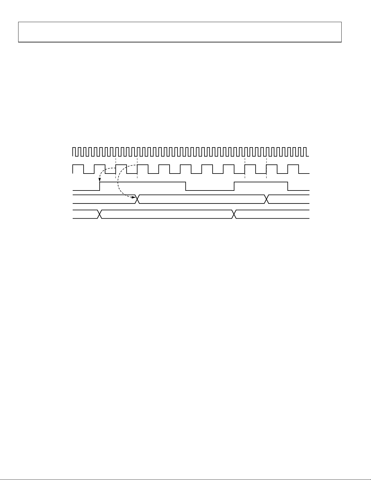
AD9958 Data Sheet
T
I/O_UPDATE, SYNC_CLK, AND SYSTEM CLOCK RELATIONSHIPS
I/O_UPDATE and SYNC_CLK are used together to transfer
data from the serial I/O buffer to the active registers in the
device. Data in the buffer is inactive.
SYNC_CLK is a rising edge active signal. It is derived from
the system clock and a divide-by-4 frequency divider. The
SYNC_CLK, which is externally provided, can be used to
synchronize external hardware to the AD9958 internal clocks.
I/O_UPDATE initiates the start of a buffer transfer. It can be
sent synchronously or asynchronously relative to the SYNC_CLK.
SYSCLK
AB
SYNC_CL K
I/O_UPDATE
If the setup time between these signals is met, then constant
latency (pipeline) to the DAC output exists. For example, if
repetitive changes to phase offset via the SPI port is desired, the
latency of those changes to the DAC output is constant; otherwise,
a time uncertainty of one SYNC_CLK period is present.
The I/O_UPDATE is essentially oversampled by the SYNC_CLK.
Therefore, I/O_UPDATE must have a minimum pulse width
greater than one SYNC_CLK period.
The timing diagram shown in Figure 40 depicts when data in
the buffer is transferred to the active registers.
DATA IN
REGIS TERS
DATA IN
I/O BUFFERS
HE DEVICE REGI STERS AN I/ O UPDATE AT PO INT A. THE DATA IS TRANSFERRED FROM THE ASYNCHRONOUSLY L OADED I/O BUF FERS AT POINT B.
N – 1
N
Figure 40. I/O_UPDATE Transferring Data from I/O Buffer to Active Registers
N + 1 N + 2
NN + 1
05252-149
Rev. C | Page 30 of 44
Page 31
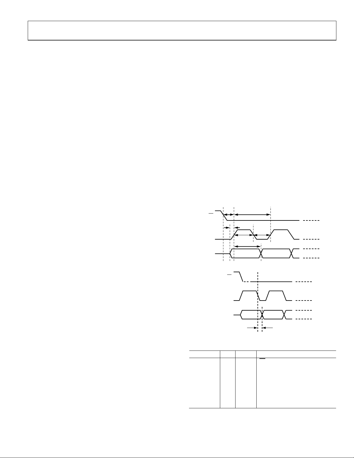
Data Sheet AD9958
SERIAL I/O PORT
OVERVIEW
The AD9958 serial I/O port offers multiple configurations to
provide significant flexibility. The serial I/O port offers an SPIcompatible mode of operation that is virtually identical to the
SPI operation found in earlier Analog Devices DDS products.
The flexibility is provided by four data pins (SDIO_0, SDIO_1,
SDIO_2, SDIO_3) that allow four programmable modes of
serial I/O operation.
Three of the four data pins (SDIO_1, SDIO_2, SDIO_3) can be
used for functions other than serial I/O port operation. These pins
can also be used to initiate a ramp-up or ramp-down (RU/RD)
of the 10-bit amplitude output scalar. In addition, SDIO_3 can
be used to provide the SYNC_I/O function that resynchronizes
the serial I/O port controller if it is out of proper sequence.
The maximum speed of the serial I/O port SCLK is 200 MHz,
but the four data pins (SDIO_0, SDIO_1, SDIO_2, SDIO_3)
can be used to further increase data throughput. The maximum
data throughput using all the SDIO pins (SDIO_0, SDIO_1,
SDIO_2, SDIO_3) is 800 Mbps.
Note that both channels share Register 0x03 to Register 0x18,
which are shown in the Register Maps and Bit Descriptions
section. This address sharing enables both DDS channels to be
written to simultaneously. For example, if a common frequency
tuning word is desired for both channels, it can be written once
through the serial I/O port to both channels. This is the default
mode of operation (all channels enabled). To enable each channel
to be independent, the two channel enable bits found in the
channel select register (CSR, Register 0x00) must be used.
There are effectively four sets or copies of addresses (Register 0x03
to Register 0x18) that the channel enable bits can access to provide
channel independence. See the Descriptions for Control Registers
section for further details of programming channels that are
common to or independent from each other. To properly read
back Register 0x03 to Register 0x18, the user must enable only
one channel enable bit at a time.
Serial operation of the AD9958 occurs at the register level,
not the byte level; that is, the controller expects that all bytes
contained in the register address are accessed. The SYNC_I/O
function can be used to abort an I/O operation, thereby allowing
fewer than all bytes to be accessed. This feature can be used to
program only a part of the addressed register. Note that only
completed bytes are affected.
There are two phases to a serial communications cycle. Phase 1
is the instruction cycle, which writes the instruction byte into
the AD9958. Each bit of the instruction byte is registered on
each corresponding rising edge of SCLK. The instruction byte
defines whether the upcoming data transfer is a write or read
operation. The instruction byte contains the serial address of
the address register.
Phase 2 of the I/O cycle consists of the actual data transfer
(write/read) between the serial port controller and the serial
port buffer. The number of bytes transferred during this phase
of the communication cycle is a function of the register being
accessed. The actual number of additional SCLK rising edges
required for the data transfer and instruction byte depends on
the number of bytes in the register and the serial I/O mode of
operation.
For example, when accessing Function Register 1 (FR1), which
is three bytes wide, Phase 2 of the I/O cycle requires that three
bytes be transferred. After transferring all data bytes per the
instruction byte, the communication cycle is completed for that
register.
At the completion of a communication cycle, the AD9958 serial
port controller expects the next set of rising SCLK edges to be
the instruction byte for the next communication cycle. All data
written to the AD9958 is registered on the rising edge of SCLK.
Data is read on the falling edge of SCLK (see Figure 43 through
Figure 49). The timing specifications for Figure 41 and Figure 42
are described in Table 25.
t
CS
SCLK
SDIO_x
SDO (SDIO_2)
PRE
Figure 41. Setup and Hold Timing for the Serial I/O Port
CS
SCLK
SDIO_x
Figure 42. Timing Diagram for Data Read for Serial I/O Port
t
DSU
t
SCLKPWH
t
DHLD
t
SCLK
t
SCLKPWL
05252-123
t
DV
05252-124
Table 25. Timing Specifications
Parameter Min Unit Description
t
1.0 ns min
PRE
t
5.0 ns min Period of serial data clock
SCLK
t
2.2 ns min Serial data setup time
DSU
t
2.2 ns min Serial data clock pulse width high
SCLKPWH
t
1.6 ns min Serial data clock pulse width low
SCLKPWL
t
0 ns min Serial data hold time
DHLD
setup time
CS
tDV 12 ns min Data valid time
Rev. C | Page 31 of 44
Page 32

AD9958 Data Sheet
D5
Each set of communication cycles does not require an I/O update
to be issued. The I/O update transfers data from the I/O port
buffer to active registers. The I/O update can be sent for each
communication cycle or can be sent when all serial operations
are complete. However, data is not active until an I/O update is
sent, with the exception of the channel enable bits in the channel
select register (CSR). These bits do not require an I/O update to
be enabled.
INSTRUCTION BYTE DESCRIPTION
The instruction byte contains the following information:
MSB LSB
D7 D6 D5 D4 D3 D2 D1 D0
1
R/W
1
x = don’t care bit.
x
x
1
A4 A3 A2 A1 A0
Bit D7 of the instruction byte (R/W) determines whether a read
or write data transfer occurs after the instruction byte write. A
logic high indicates a read operation. A logic low indicates a
write operation.
Bit D4 to Bit D0 of the instruction byte determine which register is
accessed during the data transfer portion of the communication
cycle. The internal byte addresses are generated by the AD9958.
SERIAL I/O PORT PIN DESCRIPTION
Serial Data Clock (SCLK)
The serial data clock pin is used to synchronize data to and
from the internal state machines of the AD9958. The maximum
SCLK toggle frequency is 200 MHz.
Chip Select (CS)
The chip select pin allows more than one AD9958 device to be
on the same set of serial communications lines. The chip select
is an active low enable pin. SDIO_x inputs go to a high impedance state when
communication cycle, that cycle is suspended until
reactivated low. The
CS
is high. If CS is driven high during any
CS
pin can be tied low in systems that
CS
is
maintain control of SCLK.
Serial Data I/O (SDIO_x)
Of the four SDIO pins, only the SDIO_0 pin is a dedicated SDIO
pin. SDIO_1, SDIO_2, and SDIO_3 can also be used to ramp
up/ramp down the output amplitude. Bits[2:1] in the channel
select register (CSR, Register 0x00) control the configuration
of these pins. See the Serial I/O Modes of Operation for more
information.
SERIAL I/O PORT FUNCTION DESCRIPTION
Serial Data Out (SDO)
The SDO function is available in single-bit (3-wire) mode only.
In SDO mode, data is read from the SDIO_2 pin for protocols
that use separate lines for transmitting and receiving data (see
Tabl e 26 for pin configuration options). Bits[2:1] in the channel
select register (CSR, Register 0x00) control the configuration of
this pin. The SDO function is not available in 2-bit or 4-bit serial
I/O modes.
SYNC_I/O
The SYNC_I/O function is available in 1-bit and 2-bit modes.
SDIO_3 serves as the SYNC_I/O pin when this function is
active. Bits CSR[2:1] control the configuration of this pin.
Otherwise, the SYNC_I/O function is used to synchronize the
I/O port state machines without affecting the addressable register
contents. An active high input on the SYNC_I/O (SDIO_3) pin
causes the current communication cycle to abort. After SDIO_3
returns low (Logic 0), another communication cycle can begin,
starting with the instruction byte write. The SYNC_I/O function is
not available in 4-bit serial I/O mode.
MSB/LSB TRANSFER DESCRIPTION
The AD9958 serial port can support both most significant bit
(MSB) first or least significant bit (LSB) first data formats. This
functionality is controlled by CSR[0]. MSB first is the default
mode. When CSR[0] is set high, the AD9958 serial port is in
LSB first format. The instruction byte must be written in the
format indicated by CSR[0], that is, if the AD9958 is in LSB first
mode, the instruction byte must be written from LSB to MSB. If
the AD9958 is in MSB first mode (default), the instruction byte
must be written from MSB to LSB.
Example Operation
To write Function Register 1 (FR1, Register 0x01) in MSB first
format, apply an instruction byte of 00000001 starting with the
MSB (in the following example instruction byte, the MSB is
D7). From this instruction, the internal controller recognizes a
write transfer of three bytes starting with the MSB, FR1[23].
Bytes are written on each consecutive rising SCLK edge until
Bit 0 is transferred. When the last data bit is written, the I/O
communication cycle is complete and the next byte is considered
an instruction byte.
Example Instruction Byte1
MSB
D7 D6
0 0
1
Note that the bit values are for example purposes only.
0
To write Function Register 1 (FR1) in LSB first format, apply an
instruction byte of 00000001, starting with the LSB bit (in the
preceding example instruction byte, the LSB is D0). From this
instruction, the internal controller recognizes a write transfer of
three bytes, starting with the LSB, FR1[0]. Bytes are written on
each consecutive rising SCLK edge until Bit 23 is transferred.
When the last data bit is written, the I/O communication cycle is
complete and the next byte is considered an instruction byte.
LSB
D4 D3 D2 D1 D0
0 0 0 0 1
Rev. C | Page 32 of 44
Page 33
Data Sheet AD9958
SDIO_1
Not used for
Not used for
Serial data
Serial
00
Single-bit serial mode (2-wire mode)
01
Single-bit serial mode (3-wire mode)
SERIAL I/O MODES OF OPERATION
The following are the four programmable modes of serial I/O
port operation:
• Single-bit serial 2-wire mode (default mode)
• Single-bit serial 3-wire mode
• 2-bit serial mode
• 4-bit serial mode (SYNC_I/O not available)
Tabl e 26 displays the function of all six serial I/O interface pins,
depending on the mode of serial I/O operation programmed.
Table 26. Serial I/O Port Pin Function vs. Serial I/O Mode
Single-Bit
Pin
SCLK Serial clock Serial clock Serial clock Serial
CS
SDIO_0 Serial data I/O Serial data in Serial data
SDIO_2 Not used for
SDIO_3 SYNC_I/O SYNC_I/O SYNC_I/O Serial
1
In serial mode, these pins (SDIO_0/SDIO_1/SDIO_2/SDIO_3) can be used for
RU/RD operation
Serial 2-Wire
Mode
Chip select Chip select Chip select Chip
SDIO1
1
SDIO
.
The two bits in the channel select register, CSR[2:1], set the
serial I/O mode of operation and are defined in Table 27.
Table 27. Serial I/O Mode of Operation
Serial I/O Mode Select
(CSR[2:1]) Mode of Operation
10 2-bit serial mode
11 4-bit serial mode
Single-Bit Serial (2-Wire and 3-Wire) Modes
The single-bit serial mode interface allows read/write access to
all registers that configure the AD9958. MSB first or LSB first
transfer formats are supported. In addition, the single-bit serial
mode interface port can be configured either as a single pin I/O,
which allows a 2-wire interface, or as two unidirectional pins
for input/output, which enable a 3-wire interface. Single-bit
mode allows the use of the SYNC_I/O function.
Single-Bit
Serial 3-Wire
Mode
SDIO1
Serial data
out (SDO)
2-Bit Serial Mode
I/O
I/O
Not used
for SDIO1
4-Bit Serial Mode
clock
select
Serial
data I/O
data I/O
Serial
data I/O
data I/O
In single-bit serial mode, 2-wire interface operation, the
SDIO_0 pin is the single serial data I/O pin. In single-bit serial
mode 3-wire interface operation, the SDIO_0 pin is the serial
data input pin and the SDIO_2 pin is the output data pin.
Regardless of the number of wires used in the interface, the
SDIO_3 pin is configured as an input and operates as the
SYNC_I/O pin in the single-bit serial mode and 2-bit serial
mode. The SDIO_1 pin is unused in this mode (see Table 26).
2-Bit Serial Mode
The SPI port operation in 2-bit serial mode is identical to the
SPI port operation in single-bit serial mode, except that two bits
of data are registered on each rising edge of SCLK. Therefore, it
only takes four clock cycles to transfer eight bits of information.
The SDIO_0 pin contains the even numbered data bits using
the notation D[7:0], and the SDIO_1 pin contains the odd
numbered data bits. This even and odd numbered pin/data
alignment is valid in both MSB and LSB first formats (see
Figure 44).
4-Bit Serial Mode
The SPI port in 4-bit serial mode is identical to the SPI port in
single-bit serial mode, except that four bits of data are registered
on each rising edge of SCLK. Therefore, it takes only two clock
cycles to transfer eight bits of information. The SDIO_0 and
SDIO_2 pins contain even numbered data bits using the notation
D[7:0], and the SDIO_0 pin contains the LSB of the nibble. The
SDIO_1 and SDIO_3 pins contain the odd numbered data bits,
and the SDIO_1 pin contains the LSB of the nibble to be accessed.
Note that when programming the device for 4-bit serial mode,
it is important to keep the SDIO_3 pin at Logic 0 until the device is
programmed out of the single-bit serial mode. Failure to do so
can result in the serial I/O port controller being out of
sequence.
Figure 43 through Figure 45 represent write timing diagrams
for each of the serial I/O modes available. Both MSB and LSB
first modes are shown. LSB first bits are shown in parentheses.
The clock stall low/high feature shown is not required. It is used
to show that data (SDIO) must have the proper setup time
relative to the rising edge of SCLK.
Figure 46 through Figure 49 represent read timing diagrams for
each of the serial I/O modes available. Both MSB and LSB first
modes are shown. LSB first bits are shown in parentheses. The
clock stall low/high feature shown is not required. It is used to
show that data (SDIO) must have the proper setup time relative
to the rising edge of SCLK for the instruction byte and the read
data that follows the falling edge of SCLK.
Rev. C | Page 33 of 44
Page 34
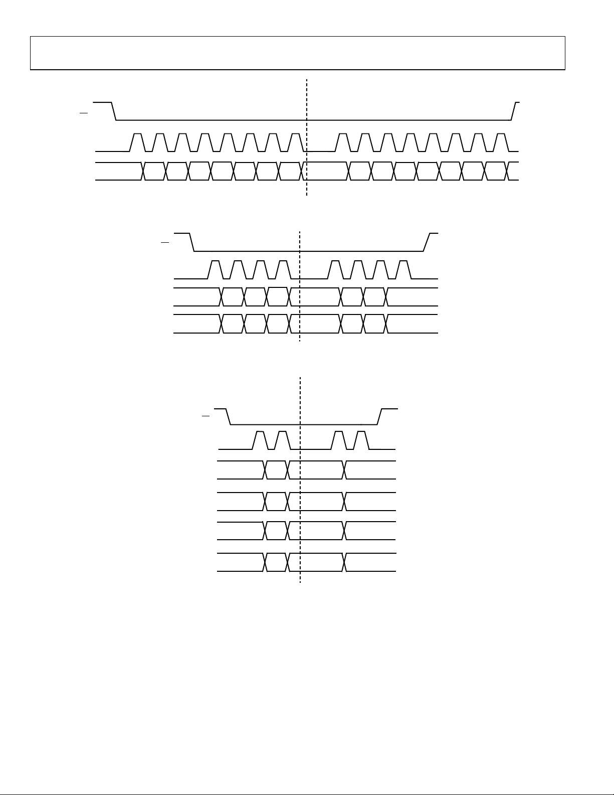
AD9958 Data Sheet
SCLK
SDIO_0
INSTRUCTI ON CYCLE
DAT
A
TRANSFER CYCL E
CS
I7
(I0)
I6
(I1)
I5
(I2)
I4
(I3)
I3
(I4)
I2
(I5)
I1
(I6)
I0
(I7)
D7
(D0)
D6
(D1)
D5
(D2)
D4
(D3)
D3
(D4)
D2
(D5)
D1
(D6)
D0
(D7)
05252-125
INSTRUCTI ON CYCLE DATA TRANS FER CYCLE
CS
SCLK
SDIO_1
SDIO_0
I7
(I1)I5(I3)I3(I5)
I1
(I7)
D7
(D1)D5(D3)D3(D5)D1(D7)
I6
(I0)
I4
(I2)I2(I4)I0(I6)
D6
(D0)D4(D2)D2(D4)D0(D6)
05252-126
INSTRUCTI ON CYCLE DATA TRANSFER CYCLE
SCLK
SDIO_1
SDIO_0
SDIO_2
SDIO_3
CS
I7
(I3)
I1
(I5)
I5
(I1)
I3
(I7)
I6
(I2)
I0
(I4)
I4
(I0)
I2
(I6)
D7
(D3)
D1
(D5)
D5
(D1)
D3
(D7)
D6
(D2)
D0
(D4)
D4
(D0)
D2
(D6)
05252-127
Figure 43. Single-Bit Serial Mode Write Timing—Clock Stall Low
Figure 44. 2-Bit Serial Mode Write Timing—Clock Stall Low
Figure 45. 4-Bit Serial Mode Write Timing—Clock Stall Low
Rev. C | Page 34 of 44
Page 35
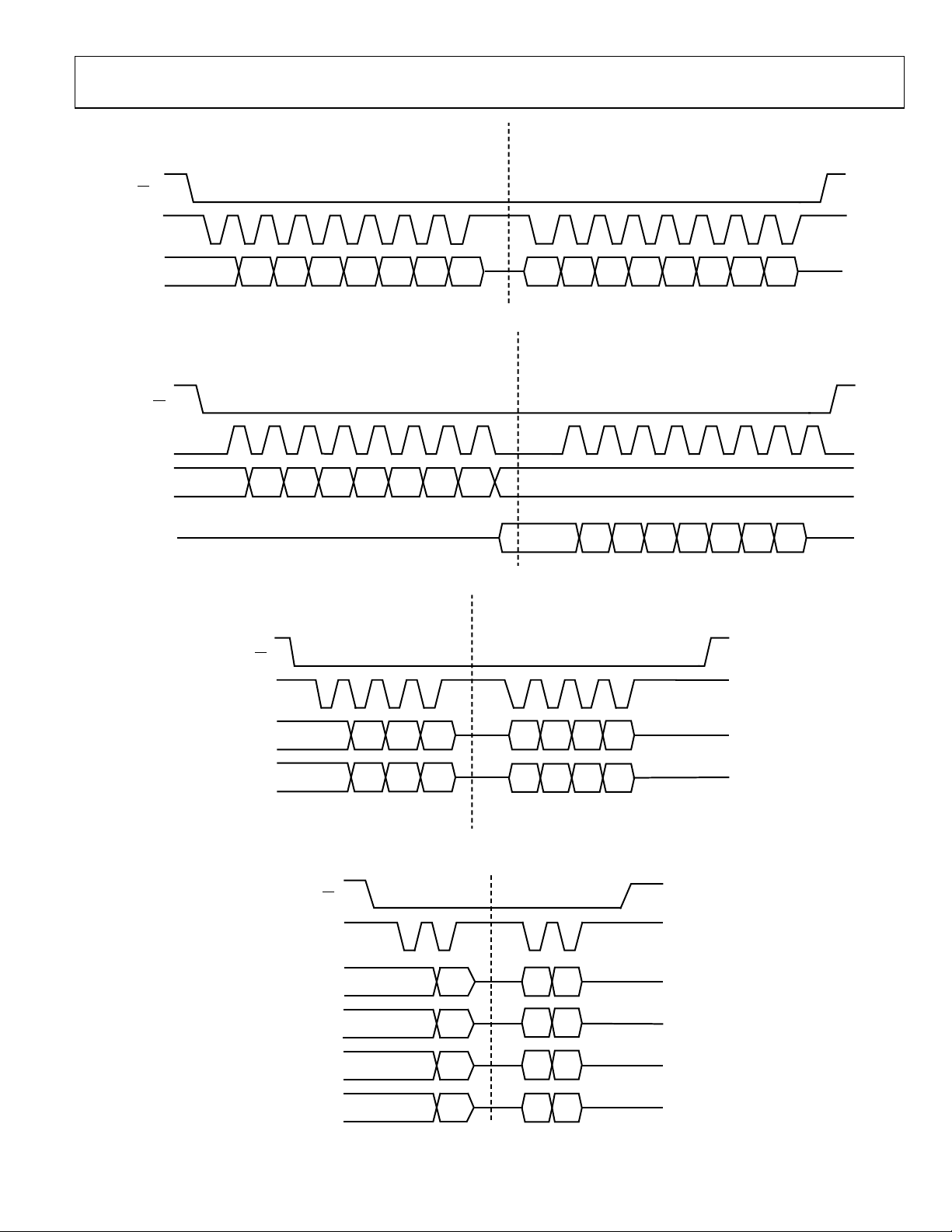
Data Sheet AD9958
INSTRUCTI ON CYCLE
DATA TRANSFER CY CLE
I7
(I0)
SDIO_0
SCLK
CS
I6
(I1)
I5
(I2)
I4
(I3)
I3
(I4)I2(I5)I1(I6)I0(I7)
D7
(D0)D6(D1)D5(D2)D4(D3)D3(D4)D2(D5)D1(D6)
D0
(D7)
05252-128
INSTRUCTI ON CYCLE
DATA TRANSFER CY CLE
SDIO_0
SCLK
CS
DON'T CARE
SDO
(SDIO_2 PI N)
I7
(I0)I6(I1)I5(I2)I4(I3)I3(I4)I2(I5)I1(I6)I0(I7)
D7
(D0)D6(D1)D5(D2)D4(D3)D3(D4)D2(D5)D1(D6)D0(D7)
05252-129
INSTRUCTI ON CYCLE
DATA TRANSFER CY CLE
SCLK
SDIO_1
SDIO_0
CS
D7
(D1)D5(D3)D3(D5)D1(D7)
D6
(D0)D4(D2)D2(D4)D0(D6)
I6
(I0)I4(I2)I2(I4)I0(I6)
I7
(I1)I5(I3)I3(I5)I1(I7)
05252-130
INSTRUCTI ON CYCLE DATA TRANSFER CYCL E
I7
(I3)
I1
(I5)
I5
(I1)
I3
(I7)
I6
(I2)
I0
(I4)
I4
(I0)
I2
(I6)
SCLK
SDIO_0
SDIO_1
SDIO_2
CS
SDIO_3
D7
(D3)
D1
(D5)
D5
(D1)
D3
(D7)
D6
(D2)
D0
(D4)
D4
(D0)
D2
(I6)
05252-131
Figure 46. Single-Bit Serial Mode (2-Wire) Read Timing—Clock Stall High
Figure 47. Single-Bit Serial Mode (3-Wire) Read Timing—Clock Stall Low
Figure 48. 2-Bit Serial Mode Read Timing—Clock Stall High
Figure 49. 4-Bit Serial Mode Read Timing—Clock Stall High
Rev. C | Page 35 of 44
Page 36

AD9958 Data Sheet
Auto sync
Multidevice sync
Multidevice sync
Multidevice sync
System clock
REGISTER MAPS AND BIT DESCRIPTIONS
REGISTER MAPS
Table 28. Control Register Map
Register
Name
(Serial
Address)
Channel
Select
Register
(CSR)
(0x00)
Function
Register 1
(FR1)
(0x01)
[15:8] Open Profile pin configuration (PPC)[14:12]
[7:0]
Function
Register 2
(FR2)
(0x02)
[7:0]
1
Channel enable bits do not require an I/O update to be activated. These bits are active immediately after the byte containing the bits is written. All other bits need an
I/O update to become active. The two channel enable bits shown in Table 28 are used to enable/disable any combination of the two channels. The default for both
channels is enabled. In readback mode, enable one channel enable bit at a time.
2
This bit must be disabled (Logic 0) in readback mode.
In the channel select register, if the user wants two different
frequencies for the two DDS channels, use the following
protocol:
Bit
Range
[7:0]
[23:16]
[15:8]
Bit 7
(MSB) Bit 6 Bit 5 Bit 4 Bit 3 Bit 2 Bit 1
Channel 1
1
enable
VCO gain
control
Reference
clock input
power-down
All channels
autoclear
sweep
accumulator
enable
Channel 0
enable1
External powerdown mode
All channels
clear wweep
accumulator
master enable
2
Open2
Open
PLL divider ratio[22:18]
SYNC_CLK
disable
All channels
autoclear phase
accumulator
status
1. Enable (Logic 1) the Channel 0 enable bit, which is
located in the channel select register, and disable the
Channel 1 enable bit (Logic 0).
2. Write the desired frequency tuning word for Channel
0, as described in Step 1, and then disable the Channel
0 enable bit (Logic 0).
Bit 0
(LSB)
Must
be 0
Ramp-up/
ramp-down
(RU/RD)[11:10]
DAC reference
power-down
All channels
clear phase
accumulator
mask
Open[3:2]
Open[3:2]
Serial I/O mode
select[2:1]
Charge pump
control[17:16]
Modulation level[9:8] 0x00
Manual
hardware
sync
Open[11:8] 0x00
LSB first 0xF0
Manual
software
sync
offset[1:0]
3. Enable the Channel 1 enable bit only, located in the
channel select Register.
4. Write the desired frequency tuning word for Channel
1 in Step 3.
Default
Value
0x00
0x00
0x00
Rev. C | Page 36 of 44
Page 37
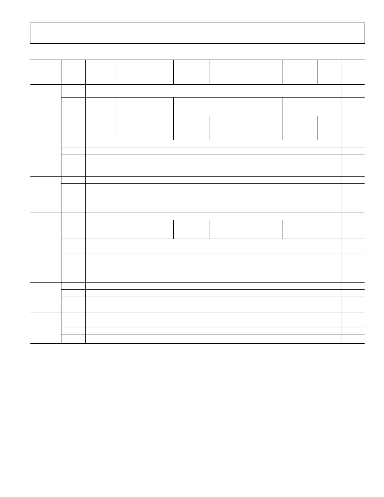
Data Sheet AD9958
[7:0]
Digital
DAC
Matched
Autoclear
Clear sweep
Autoclear
Clear phase
Sine
0x02
Increment/decrement
Amplitude
Ramp-up/
Load ARR at
Amplitude scale
LSR Falling
Table 29. Channel Register Map
Register
Name
(Serial
Address)
Channel
Function
Register
(CFR)
(0x03)
Bit
Range
[23:16]
1
[15:8]
Bit 7
(MSB)
Bit 6 Bit 5 Bit 4 Bit 3 Bit 2 Bit 1
Amplitude freq. phase
(AFP) select[23:22]
Linear
sweep
no-dwell
Linear
sweep
enable
Load SRR at
I/O_UPDATE
Open[21:16] 0x00
Open[12:11] Must be 0
Bit 0
(LSB)
DAC full-scale current
control[9:8]
Default
Value
0x03
powerdown
powerdown
pipe delays
active
sweep
accumulator
accumulator
phase
accumulator
accumulator2
wave
output
enable
Channel
Frequency
Tuning
Word 0
(CFTW0)
[31:24] Frequency Tuning Word 0[31:24] 0x00
[23:16] Frequency Tuning Word 0[23:16] N/A
[15:8] Frequency Tuning Word 0[15:8] N/A
1
[7:0] Frequency Tuning Word 0[7:0] N/A
(0x04)
Channel
Phase
Offset
Word 0
[15:8] Open[15:14] Phase Offset Word 0[13:8] 0x00
[7:0] Phase Offset Word 0[7:0] 0x00
1
(CPOW0)
(0x05)
Amplitude
Control
Register
(ACR)
(0x06)
Linear
Sweep
Ramp
1
Rate
[23:16] Amplitude Ramp Rate[23:16] N/A
[15:8]
step size[15:14]
Open
multiplier
enable
ramp-down
enable
I/O_UPDATE
factor[9:8]
0x00
[7:0] Amplitude scale factor[7:0] 0x00
[15:8] Falling sweep ramp rate (FSRR)[15:8] N/A
[7:0] Rising sweep ramp rate (RSRR)[7:0] N/A
(LSRR)
(0x07)
LSR Rising
Delta
1
Word
(RDW)
(0x08)
[31:24] Rising delta word[31:24] N/A
[23:16] Rising delta word[23:16] N/A
[15:8] Rising delta word[15:8] N/A
[7:0] Rising delta word[7:0] N/A
[31:24] Falling delta word[31:24] N/A
Delta
1
Word
(FDW)
(0x09)
1
There are two sets of channel registers and profile registers, one per channel. This is not shown in the Table 29 or Table 30 because the addresses of all channel
registers and profile registers are the same for each channel. Therefore, the channel enable bits (CSR[7:6]) determine if the channel registers and/or profile registers of
each channel are written to or not.
2
The clear phase accumulator bit (CFR[1]) is set to Logic 1 after a master reset. It self-clears or is set to Logic 0 when an I/O update is asserted.
[23:16] Falling delta word[23:16] N/A
[15:8] Falling delta word[15:8] N/A
[7:0] Falling delta word[7:0] N/A
Rev. C | Page 37 of 44
Page 38

AD9958 Data Sheet
Channel Word 5 (CW5) (0x0E)
[31:0]
Frequency tuning word[31:0] or phase word[31:18] or amplitude word[31:22]
N/A
Table 30. Profile Register Map1
Register Name (Address)
Channel Word 1 (CW1) (0x0A) [31:0] Frequency tuning word[31:0] or phase word[31:18] or amplitude word[31:22] N/A
Channel Word 2 (CW2) (0x0B) [31:0] Frequency tuning word[31:0] or phase word[31:18] or amplitude word[31:22] N/A
Channel Word 3 (CW3) (0x0C) [31:0] Frequency tuning word[31:0] or phase word[31:18] or amplitude word[31:22] N/A
Channel Word 3 (CW4) (0x0D) [31:0] Frequency tuning word[31:0] or phase word[31:18] or amplitude word[31:22] N/A
Channel Word 6 (CW6) (0x0F) [31:0] Frequency tuning word[31:0] or phase word[31:18] or amplitude word[31:22] N/A
Channel Word 7 (CW7) (0x10) [31:0] Frequency tuning word[31:0] or phase word[31:18] or amplitude word[31:22] N/A
Channel Word 8 (CW8) (0x11) [31:0] Frequency tuning word[31:0] or phase word[31:18] or amplitude word[31:22] N/A
Channel Word 9 (CW9) (0x12) [31:0] Frequency tuning word[31:0] or phase word[31:18] or amplitude word[31:22] N/A
Channel Word 10 (CW10) (0x13) [31:0] Frequency tuning word[31:0] or phase word[31:18] or amplitude word[31:22] N/A
Channel Word 11 (CW11) (0x14) [31:0] Frequency tuning word[31:0] or phase word[31:18] or amplitude word[31:22] N/A
Channel Word 12 (CW12) (0x15) [31:0] Frequency tuning word[31:0] or phase word[31:18] or amplitude word[31:22] N/A
Channel Word 13 (CW13) (0x16) [31:0] Frequency tuning word[31:0] or phase word[31:18] or amplitude word[31:22] N/A
Channel Word 14 (CW14) (0x17) [31:0] Frequency tuning word[31:0] or phase word[31:18] or amplitude word[31:22] N/A
Channel Word 15 (CW15) (0x18) [31:0] Frequency tuning word[31:0] or phase word[31:18] or amplitude word[31:22] N/A
1
Each channel word register has a capacity of 32 bits. If phase or amplitude is stored in the channel word registers, it must be first MSB aligned per the bit range.
Only the MSB byte is shown for each channel word register.
Bit
Range
Bit 7
(MSB) Bit 6 Bit 5 Bit 4 Bit 3 Bit 2 Bit 1
Bit 0
(LSB)
Default
Value
Rev. C | Page 38 of 44
Page 39

Data Sheet AD9958
01 = only Channel 0 receives commands from the channel registers and profile registers.
22:18
PLL divider ratio
If the value is 4 or 20 (decimal) or between 4 and 20, the PLL is enabled and the value sets the
15
Open
DESCRIPTIONS FOR CONTROL REGISTERS
Channel Select Register (CSR)—Address 0x00
One byte is assigned to this register.
The CSR determines if channels are enabled or disabled by the status of the two channel enable bits. Both channels are enabled by their
default state. The CSR also determines which serial mode of operation is selected. In addition, the CSR offers a choice of MSB first or LSB
first format.
Table 31. Bit Descriptions for CSR
Bit Mnemonic Description
7:6 Channel [1:0] enable Bits are active immediately after being written. They do not require an I/O update to take effect.
There are two sets of channel registers and profile (channel word) registers, one per channel. This
is not shown in the channel register map or the profile register map. The addresses of all channel
registers and profile registers are the same for each channel. Therefore, the channel enable bits
distinguish the channel registers and profile registers values of each channel. For example,
10 = only Channel 1 receives commands from the channel registers and profile registers.
11 = both Channel 0 and Channel 1 receive commands from the channel registers and profile
registers.
5:4 Open
3 Must be 0 Must be set to 0.
2:1 Serial I/O mode select 00 = single-bit serial (2-wire mode).
01 = single-bit serial (3-wire mode).
10 = 2-bit serial mode.
11 = 4-bit serial mode.
See the Serial I/O Modes of Operation section for more details.
0 LSB first 0 = the serial interface accepts serial data in MSB first format (default).
1 = the serial interface accepts serial data in LSB first format.
Function Register 1 (FR1)—Address 0x01
Three bytes are assigned to this register. FR1 is used to control the mode of operation of the chip.
Table 32. Bit Descriptions for FR1
Bit Mnemonic Description
23 VCO gain control 0 = the low range (system clock below 160 MHz) (default).
1 = the high range (system clock above 255 MHz).
multiplication factor. If the value is outside of 4 and 20 (decimal), the PLL is disabled.
17:16 Charge pump control 00 (default) = the charge pump current is 75 µA.
01 = charge pump current is 100 µA.
10 = charge pump current is 125 µA.
11 = charge pump current is 150 µA.
14:12 Profile pin configuration (PPC) The profile pin configuration bits control the configuration of the data and SDIO_x pins for the
different modulation modes. See the Modulation Mode section in this document for details.
11:10 Ramp-up/ramp-down (RU/RD) The RU/RD bits control the amplitude ramp-up/ramp-down time of a channel. See the Output
Amplitude Control Mode section for more details.
9:8 Modulation level The modulation (FSK, PSK, and ASK) level bits control the level (2/4/8/16) of modulation to be
performed for a channel. See the Modulation Mode section for more details.
7 Reference clock input 0 = the clock input circuitry is enabled for operation (default).
power-down 1 = the clock input circuitry is disabled and is in a low power dissipation state.
Rev. C | Page 39 of 44
Page 40

AD9958 Data Sheet
down.
1 = the external power-down mode is in full power-down mode. In this mode, when the
PWR_DWN_CTL input pin is high, all functions are powered down. This includes the DAC and PLL,
1 = the manual hardware synchronization feature of multiple devices is active.
sweep accumulator
1 = the sweep accumulator memory elements for both channels are asynchronously cleared.
4
Multidevice sync mask
See the Synchronizing Multiple AD9958 Devices section for more details.
Bit Mnemonic Description
6 External power-down mode 0 = the external power-down mode is in fast recovery power-down mode (default). In this mode,
when the PWR_DWN_CTL input pin is high, the digital logic and the DAC digital logic are
powered down. The DAC bias circuitry, PLL, oscillator, and clock input circuitry are not powered
which take a significant amount of time to power up.
5 SYNC_CLK disable 0 = the SYNC_CLK pin is active (default).
1 = the SYNC_CLK pin assumes a static Logic 0 state (disabled). In this state, the pin drive logic is
shut down. However, the synchronization circuitry remains active internally to maintain normal
device operation.
4 DAC reference power-down 0 = DAC reference is enabled (default).
1 = DAC reference is powered down.
3:2 Open See the Synchronizing Multiple AD9958 Devices section for details.
1 Manual hardware sync 0 = the manual hardware synchronization feature of multiple devices is inactive (default).
0 Manual software sync 0 = the manual software synchronization feature of multiple devices is inactive (default).
1 = the manual software synchronization feature of multiple devices is active. See the
Synchronizing Multiple AD9958 Devices section for details.
Function Register 2 (FR2)—Address 0x02
Two bytes are assigned to this register. The FR2 is used to control the various functions, features, and modes of the AD9958.
Table 33. Bit Descriptions for FR2
Bit Mnemonic Description
15 All channels autoclear sweep
accumulator
1 = this bit automatically and synchronously clears (loads 0s into) the sweep accumulator for one
14 All channels clear 0 = the sweep accumulator functions as normal (default).
13 All channels autoclear phase
accumulator
1 = this bit automatically and synchronously clears (loads 0s into) the phase accumulator for one
12 All channels clear phase 0 = the phase accumulator functions as normal (default).
Accumulator 1 = the phase accumulator memory elements for both channels are asynchronously cleared.
11:8 Open
7 Auto sync enable See the Synchronizing Multiple AD9958 Devices section for more details.
6 Multidevice sync master enable See the Synchronizing Multiple AD9958 Devices section for more details.
5 Multidevice sync status See the Synchronizing Multiple AD9958 Devices section for more details.
3: 2 Open
1:0 System clock offset See the Synchronizing Multiple AD9958 Devices section for more details.
0 = a new delta word is applied to the input, as in normal operation, but not loaded into the
accumulator (default).
cycle upon reception of the I/O_UPDATE sequence indicator on both channels.
0 = a new frequency tuning word is applied to the inputs of the phase accumulator, but not
loaded into the accumulator (default).
cycle upon receipt of the I/O update sequence indicator on both channels.
Rev. C | Page 40 of 44
Page 41

Data Sheet AD9958
0
Sine wave output
0 = the angle-to-amplitude conversion logic employs a cosine function (default).
DESCRIPTIONS FOR CHANNEL REGISTERS
Channel Function Register (CFR)—Address 0x03
Three bytes are assigned to this register.
Table 34. Bit Descriptions for CFR
Bit Mnemonic Description
23:22 Amplitude frequency
phase (AFP) select
21:16 Open
15 Linear sweep no-dwell 0 = the linear sweep no-dwell function is inactive (default).
1 = the linear sweep no-dwell function is active. If CFR[15] is active, the linear sweep no-dwell function is
14 Linear sweep enable 0 = the linear sweep capability is inactive (default).
1 = the linear sweep capability is enabled. When enabled, the delta frequency tuning word is applied to
13 Load SRR at
I/O_UPDATE
1 = the linear sweep ramp rate timer is loaded upon timeout (timer = 1) or at the time of an I/O_UPDATE
12:11 Open
10 Must be 0 Must be set to 0.
9:8 DAC full-scale current
control
7 Digital power-down 0 = the digital core is enabled for operation (default).
1 = the digital core is disabled and is in its lowest power dissipation state.
6 DAC power-down 0 = the DAC is enabled for operation (default).
1 = the DAC is disabled and is in its lowest power dissipation state.
5 Matched pipe delays 0 = matched pipe delay mode is inactive (default).
active 1 = matched pipe delay mode is active. See the Single-Tone Mode—Matched Pipeline Delay section for
4 Autoclear sweep
accumulator
1 = the sweep accumulator is automatically and synchronously cleared for one cycle upon receipt of an
3 Clear sweep 0 = the sweep accumulator functions as normal (default).
accumulator 1 = the sweep accumulator memory elements are asynchronously cleared.
2 Autoclear phase
accumulator
1 = the phase accumulator is automatically and synchronously cleared for one cycle upon receipt of an
1 Clear phase 0 = the phase accumulator functions as normal (default).
accumulator 1 = the phase accumulator memory elements are asynchronously cleared.
Controls what type of modulation is to be performed for that channel. See the Modulation Mode section
for details.
activated. See the Linear Sweep Mode section for details. If CFR[14] is clear, this bit is don’t care.
the frequency accumulator at the programmed ramp rate.
0 = the linear sweep ramp rate timer is loaded only upon timeout (timer = 1) and is not loaded because
of an I/O_UPDATE input signal (default).
input signal.
11 = the DAC is at the largest LSB value (default).
See Table 5 for other settings.
details.
0 = the current state of the sweep accumulator is not impacted by receipt of an I/O_UPDATE signal
(default).
I/O_UPDATE signal.
0 = the current state of the phase accumulator is not impacted by receipt of an I/O_UPDATE signal
(default).
I/O_UPDATE signal.
enable 1 = the angle-to-amplitude conversion logic employs a sine function.
Rev. C | Page 41 of 44
Page 42

AD9958 Data Sheet
Channel Frequency Tuning Word 0 (CFTW0)—Address 0x04
Four bytes are assigned to this register.
Table 35. Description for CFTW0
Bit Mnemonic Description
31:0 Frequency Tuning Word 0 Frequency Tuning Word 0 for each channel.
Channel Phase Offset Word 0 (CPOW0)—Address 0x05
Two bytes are assigned to this register.
Table 36. Description for CPOW0
Bit Mnemonic Description
15:14 Open
13:0 Phase Offset Word 0 Phase Offset Word 0 for each channel.
Amplitude Control Register (ACR)—Address 0x06
Three bytes are assigned to this register.
Table 37. Description for ACR
Bit Mnemonic Description
23:16 Amplitude ramp rate Amplitude ramp rate value.
15:14 Increment/decrement
step size
13 Open
12 Amplitude multiplier
enable
1 = amplitude multiplier is enabled.
11 Ramp-up/ramp-down This bit is valid only when ACR[12] is active high.
enable 0 = when ACR[12] is active, Logic 0 on ACR[11] enables the manual RU/RD operation. See the
1 = if ACR[12] is active, a Logic 1 on ACR[11] enables the auto RU/RD operation. See the Output
10 Load ARR at
I/O_UPDATE
1 = the amplitude ramp rate timer is loaded upon timeout (timer = 1) or at the time of an
9:0 Amplitude scale factor Amplitude scale factor for each channel.
Amplitude increment/decrement step size.
0 = amplitude multiplier is disabled. The clocks to this scaling function (auto RU/RD) are stopped
for power saving, and the data from the DDS core is routed around the multipliers (default).
Output Amplitude Control Mode section for details (default).
Amplitude Control Mode section for details.
0 = the amplitude ramp rate timer is loaded only upon timeout (timer = 1) and is not loaded due
to an I/O_UPDATE input signal (default).
I/O_UPDATE input signal.
Rev. C | Page 42 of 44
Page 43

Data Sheet AD9958
Linear Sweep Ramp Rate (LSRR)—Address 0x07
Two bytes are assigned to this register.
Table 38. Description for LSRR
Bit Mnemonic Description
15:8 Falling sweep ramp rate (FSRR) Linear falling sweep ramp rate.
7:0 Rising sweep ramp rate (RSRR) Linear rising sweep ramp rate.
LSR Rising Delta Word (RDW)—Address 0x08
Four bytes are assigned to this register.
Table 39. Description for RDW
Bit Mnemonic Description
31:0 Rising delta word 32-bit rising delta-tuning word.
LSR Falling Delta Word (FDW)—Address 0x09
Four bytes are assigned to this register.
Table 40. Description for FDW
Bit Mnemonic Description
31:0 Falling delta word 32-bit falling delta-tuning word.
Rev. C | Page 43 of 44
Page 44
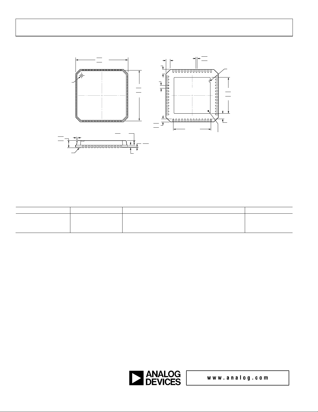
AD9958 Data Sheet
COMPLIANT TO JEDEC STANDARDS MO-220-V LLD-2
TOP VIEW
SIDE VIEW
1
56
14
15
43
42
28
29
0.50
0.40
0.30
0.30
0.23
0.18
0.20 REF
12° MAX
1.00
0.85
0.80
6.50 REF
SEATING
PLANE
0.60 MAX
0.60
MAX
COPLANARITY
0.08
0.05 MAX
0.02 NOM
0.25 MIN
FOR PROPE R CONNECTION OF
THE EXPOSED PAD, REFER TO
THE PIN CONFIGURATION AND
FUNCTIO N DE SCRIPTIO NS
SECTION OF THIS DATA SHEET.
PIN 1
INDICATOR
8.10
8.00 SQ
7.90
7.85
7.75 SQ
7.65
0.50
BSC
BOTTOM VIEW
EXPOSED
PAD
PIN 1
INDICATOR
06-07-2012-A
0.80 MAX
0.65 TYP
6.25
6.10 SQ
5.95
©2005–2016 Analog Devices, Inc. All rights reserved. Trademarks and
OUTLINE DIMENSIONS
Figure 50. 56-Lead Lead Frame Chip Scale Package [LFCSP_VQ]
8 mm × 8 mm Body, Very Thin Quad
(CP-56-1)
Dimensions shown in millimeters
ORDERING GUIDE
Model1 Temperature Range Package Description Package Option
AD9958BCPZ −40°C to +85°C 56-Lead Lead Frame Chip Scale Package [LFCSP_VQ] CP-56-1
AD9958BCPZ-REEL7 −40°C to +85°C 56-Lead Lead Frame Chip Scale Package [LFCSP_VQ] CP-56-1
AD9958/PCBZ Evaluation Board
1
Z = RoHS Compliant Part.
registered trademarks are the property of their respective owners.
D05252-0-11/16(C)
Rev. C | Page 44 of 44
 Loading...