

Page 1
Complete, Quad, 12-/14-/16-Bit, Serial Input,
Unipolar/Bipolar Voltage Output DACs
AD5724/AD5734/AD5754
Rev. F Document Feedback
Information furnished by Analog Devices is believed to be accurate and reliable. However, no
Trademarks and registered trademarks are the property of their respective owners.
Technical Support www.analog.com
06468-001
DA
C C
DAC
D
D
ACB
INP
UT
REGISTER A
IN
PUT
REGISTER B
INP
UT
REGISTER C
n
n
DAC
A
LDA
C
REF
IN
V
OUT
D
V
OUT
C
V
OUT
B
V
OUT
A
REFERENCE BUFFERS
SDI
N
S
CLK
SYN
C
S
DO
CL
R
DV
CC
GND
n
n
n
BI
N/2sCO
MP
DAC_
GND (2) SIG_G
ND (2)
AD5724/AD5734/AD5754
I
NPU
T SH
IFT
R
EGI
STE
R
AND
C
ONTROL
LOG
IC
AV
DD
AV
SS
INP
UT
REGISTER D
DAC
REGISTER A
DAC
REGISTER B
DAC
REGISTER C
DAC
REGISTER D
AD5724: n = 12-BIT
AD5734: n = 14-BIT
AD5754: n = 16-BIT
Data Sheet
FEATURES
Complete, quad, 12-/14-/16-bit digital-to-analog
converter (DAC)
Operates from single/dual supplies
Software programmable output range
+5 V, +10 V, +10.8 V, ±5 V, ±10 V, ±10.8 V
INL error: ±16 LSB maximum, DNL error: ±1 LSB maximum
Total unadjusted error (TUE): 0.1% FSR maximum
Settling time: 10 µs typical
Integrated reference buffers
Output control during power-up/brownout
Simultaneous updating via
Asynchronous
to zero scale or midscale
CLR
DSP-/microcontroller-compatible serial interface
24-lead TSSOP
Operating temperature range: −40°C to +85°C
iCMOS process technology
APPLICATIONS
Industrial automation
Closed-loop servo control, process control
Automotive test and measurement
Programmable logic controllers
LDAC
1
GENERAL DESCRIPTION
The AD5724/AD5734/AD5754 are quad, 12-/14-/16-bit, serial
input, voltage output DACs. The devices operate from singlesupply voltages from +4.5 V up to +16.5 V or dual-supply
voltages from ±4.5 V up to ±16.5 V. Nominal full-scale output
range is software-selectable from +5 V, +10 V, +10.8 V, ± 5 V,
±10 V, or ±10.8 V. Integrated output amplifiers, reference buffers,
and proprietary power-up/power-down control circuitry are also
provided.
The devices offer guaranteed monotonicity, integral
nonlinearity (INL) of ±16 LSB maximum, low noise, and 10 µs
maximum settling time.
The AD5724/AD5734/AD5754 use a serial interface that operates
at clock rates up to 30 MHz and are compatible with DSP and
microcontroller interface standards. Double buffering allows
the simultaneous updating of all DACs. The input coding is
user-selectable twos complement or offset binary for a bipolar
output (depending on the state of Pin BIN/
binary for a unipolar output. The asynchronous clear function
clears all DAC registers to a user-selectable zero-scale or midscale
output. The devices are available in a 24-lead TSSOP and offer
guaranteed specifications over the −40°C to +85°C industrial
temperature range.
2sComp
), and straight
1
For analog systems designers within industrial/instrumentation equipment OEMs that need high performance ICs at higher-voltage levels, iCMOS® is a technology
platform that enables the development of analog ICs capable of 30 V and operating at ±15 V supplies while allowing dramatic reductions in power consumption and
package size, as well as increased ac and dc performance.
responsibility is assumed by Analog Devices for its use, nor for any infringements of patents or other
rights of third parties that may result from its use. Specifications subject to change without notice. No
license is granted by implication or otherwise under any patent or patent rights of Analog Devices.
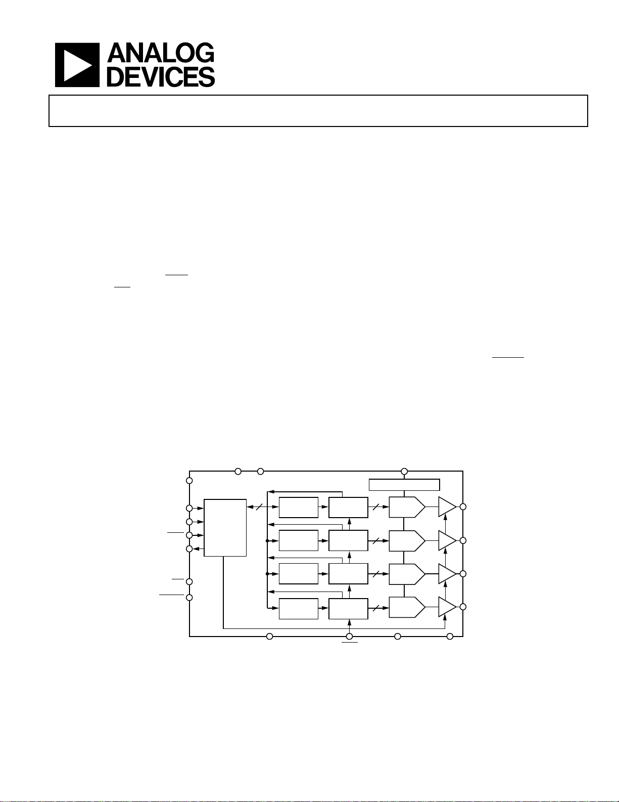
FUNCTIONAL BLOCK DIAGRAM
Figure 1.
One Technology Way, P.O. Box 9106, Norwood, MA 02062-9106, U.S.A.
Tel: 781.329.4700 ©2008–2017 Analog Devices, Inc. All rights reserved.
Page 2

AD5724/AD5734/AD5754 Data Sheet
TABLE OF CONTENTS
Features .............................................................................................. 1
Applications ....................................................................................... 1
General Description ......................................................................... 1
Functional Block Diagram .............................................................. 1
Revision History ............................................................................... 2
Specifications ..................................................................................... 3
AC Performance Characteristics ................................................ 5
Timing Characteristics ................................................................ 5
Timing Diagrams .......................................................................... 6
Absolute Maximum Ratings ............................................................ 8
ESD Caution .................................................................................. 8
Pin Configuration and Function Descriptions ............................. 9
Typical Performance Characteristics ........................................... 10
Terminology .................................................................................... 16
Theory of Operation ...................................................................... 18
Architecture ................................................................................. 18
Power-Up Sequence ................................................................... 18
Serial Interface ............................................................................ 18
Load DAC (
Asynchronous Clear (
Configuring the AD5724/AD5734/AD5754 .......................... 20
LDAC
)..................................................................... 20
CLR
) ....................................................... 20
Transfer Function ....................................................................... 20
Input Shift Register .................................................................... 24
DAC Register .............................................................................. 24
Output Range Select Register ................................................... 25
Control Register ......................................................................... 25
Power Control Register.............................................................. 26
Features ............................................................................................ 27
Analog Output Control ............................................................. 27
Power-Down Mode .................................................................... 27
Overcurrent Protection ............................................................. 27
Thermal Shutdown .................................................................... 27
Applications Information .............................................................. 28
+5 V/±5 V Operation ................................................................ 28
Alternative Power-Up Sequence Support ............................... 28
Layout Guidelines....................................................................... 28
Galvanically Isolated Interface ................................................. 29
Voltage Reference Selection ...................................................... 29
Microprocessor Interfacing ....................................................... 29
Outline Dimensions ....................................................................... 31
Ordering Guide .......................................................................... 31
REVISION HISTORY
2/2017—Rev. E to Rev. F
Added Power-Up Sequence Section ............................................. 18
Changes to Table 7 and Table 8 ..................................................... 21
Changes to Table 10 and Table 11 ................................................ 22
Changes to Table 13 and Table 14 ................................................ 23
Changes to Analog Output Control Section ............................... 27
Added Alternative Power-Up Sequence Support Section,
Figure 43, and Figure 44; Renumbered Sequentially ................. 28
2/2016—Rev. D to Rev. E
Changes to Table 1...................................................................................... 3
Change to Table 5 ......................................................................................... 9
7/2011—Rev. C to Rev. D
Changes to Table 3: t7, t8, t10 Limits ....................................................... 5
Rev. F | Page 2 of 31
3/2011—Rev. B to Rev. C
Changes to Configuring the AD5724/
Section .............................................................................................. 20
8/2010—Rev. A to Rev. B
Changes to Table 27 ....................................................................... 26
4/2010—Rev. 0 to Rev. A
Changes to Junction Temperature, T
Changes to Exposed Pad Description, Table 5 .............................. 9
Added Exposed Paddle Notation to Outline Dimensions ........ 30
8/2008—Revision 0: Initial Version
AD5734/AD5754
max Parameter, Table 4 ... 8
J
Page 3

Data Sheet AD5724/AD5734/AD5754
ACCURACY
Outputs unloaded
Total Unadjusted Error (TUE)
Offset Error TC3
±4 ppm FSR/°C
Gain Error
−0.025
+0.025
% FSR
±10 V range, TA = 25°C, error at other
SPECIFICATIONS
AVDD = 4.5 V1 to 16.5 V; AVSS = −4.5 V1 to −16.5 V, or 0 V; GND = 0 V; REFIN= 2.5 V; DVCC = 2.7 V to 5.5 V; R
C
= 200 pF; all specifications T
LOAD
MIN
to T
MAX
.
Table 1.
Parameter Min Typ Max Unit Test Conditions/Comments
Resolution
AD5754 16 Bits
AD5734 14 Bits
AD5724 12 Bits
LOAD
= 2 kΩ;
A Version −0.3 +0.3 % FSR
B Version −0.1 +0.1 % FSR
Relative Accuracy (INL)2
AD5754 −16 +16 LSB
AD5734 −4 +4 LSB
AD5724 −1 +1 LSB
Differential Nonlinearity (DNL) −1 +1 LSB All models, all versions, guaranteed monotonic
Bipolar Zero Error −6 +6 mV ±10 V range, TA = 25°C, error at other temp-
Bipolar Zero Error TC3 ±4 ppm FSR/°C
Zero-Scale Error −6 +6 mV ±10 V range, TA = 25°C, error at other temp-
Zero-Scale Error TC3 ±4 ppm FSR/°C
Offset Error −6 +6 mV +10 V range, TA = 25°C, error at other
Gain Error3 −0.065 0 % FSR +10 V and +5 V ranges, TA = 25°C, error at other
Gain Error3 0 +0.08 % FSR ±5 V range, TA = 25°C, error at other
Gain Error TC3 ±8 ppm FSR/°C
DC Crosstalk3 120 µV
REFERENCE INPUT3
Reference Input Voltage 2.5 V ±1% for specified performance
DC Input Impedance 1 5 MΩ
Input Current −2 ±0.5 +2 µA
Reference Range 2 3 V
OUTPUT CHARACTERISTICS3
Output Voltage Range −10.8 +10.8 V AVDD/AVSS = ±11.7 V min, REFIN = +2.5 V
−12 +12 V AVDD/AVSS = ±12.9 V min, REFIN = +3 V
Headroom Required 0.5 0.9 V
Output Voltage TC ±4 ppm FSR/°C
Short-Circuit Current 20 mA
Load 2 kΩ For specified performance
Capacitive Load Stability 4000 pF
DC Output Impedance 0.5 Ω
±10 V range
±10 V range
eratures obtained using bipolar zero error TC
eratures obtained using zero-scale error TC
temperatures obtained using offset error TC
temperatures obtained using gain error TC
temperatures obtained using gain error TC
temperatures obtained using gain error TC
Rev. F | Page 3 of 31
Page 4

AD5724/AD5734/AD5754 Data Sheet
Pin Capacitance
5
pF
Per pin
DVCC
2.7 5.5
V
Parameter Min Typ Max Unit Test Conditions/Comments
DIGITAL INPUTS3 DVCC = 2.7 V to 5.5 V, JEDEC compliant
Input High Voltage, VIH 2 V
Input Low Voltage, VIL 0.8 V
Input Current ±1 µA Per pin
DIGITAL OUTPUTS (SDO)3
Output Low Voltage, VOL 0.4 V DVCC = 5 V ± 10%, sinking 200 µA
Output High Voltage, VOH DVCC − 1 V DV
Output Low Voltage, VOL 0.4 V DVCC = 2.7 V to 3.6 V, sinking 200 µA
Output High Voltage, VOH DVCC − 0.5 V DVCC = 2.7 V to 3.6 V, sourcing 200 µA
High Impedance Leakage Current −1 +1 µA
High Impedance Output Capacitance 5 pF
POWER REQUIREMENTS
AVDD 4.5 16.5 V
AVSS −4.5 −16.5 V
= 5 V ± 10%, sourcing 200 µA
CC
Power Supply Sensitivity
∆V
/∆ΑVDD −65 dB
OUT
3
AIDD 2.5 mA/channel Outputs unloaded
1.75 mA/channel AVSS = 0 V, outputs unloaded
AISS 2.2 mA/channel Outputs unloaded
DICC 0.5 3 µA VIH = DVCC, VIL = GND
Power Dissipation 310 mW ±16.5 V operation, outputs unloaded
115 mW 16.5 V operation, AVSS = 0 V, outputs unloaded
Power-Down Currents
AIDD 40 µA
AISS 40 µA
DICC 300 nA
1
For specified performance, maximum headroom requirement is 0.9 V.
2
INL is measured from Code 512, Code 128, and Code 32 for the AD5754, the AD5734, and the AD5724, respectively.
3
Guaranteed by characterization; not production tested.
Rev. F | Page 4 of 31
Page 5
Data Sheet AD5724/AD5734/AD5754
DAC to DAC Crosstalk
10 nV-sec
Parameter
Limit at t
, t
Unit
Description
t12
10
µs typ
DAC output settling time
t13
20
ns min
pulse width low
AC PERFORMANCE CHARACTERISTICS
AVDD = 4.5 V1 to 16.5 V; AVSS = −4.5 V1 to −16.5 V, or 0 V; GND = 0 V; REFIN= 2.5 V; DVCC = 2.7 V to 5.5 V; R
C
= 200 pF; all specifications T
LOAD
MIN
to T
MAX
.
Table 2.
A, B Version
Parameter2 Min Typ Max Unit Test Conditions/Comments
DYNAMIC PERFORMANCE
Output Voltage Settling Time 10 12 µs 20 V step to ±0.03% FSR
7.5 8.5 µs 10 V step to ±0.03% FSR
5 µs 512 LSB step settling (16-bit resolution)
Slew Rate 3.5 V/µs
Digital-to-Analog Glitch Energy 13 nV-sec
Glitch Impulse Peak Amplitude 35 mV
Digital Crosstalk 10 nV-sec
Digital Feedthrough 0.6 nV-sec
Output Noise
0.1 Hz to 10 Hz Bandwidth 15 µV p-p 0x8000 DAC code
100 kHz Bandwidth 80 µV rms
Output Noise Spectral Density 320 nV/√Hz Measured at 10 kHz, 0x8000 DAC code
1
For specified performance, maximum headroom requirement is 0.9 V.
2
Guaranteed by design and characterization. Not production tested.
TIMING CHARACTERISTICS
AVDD = 4.5 V to 16.5 V; AVSS = −4.5 V to −16.5 V, or 0 V; GND = 0 V; REFIN = 2.5 V; DVCC = 2.7 V to 5.5 V; R
all specifications T
MIN
to T
, unless otherwise noted.
MAX
LOAD
= 2 kΩ;
LOAD
= 2 kΩ; C
= 200 pF;
LOAD
Table 3.
1, 2, 3
MIN
MAX
t1 33 ns min SCLK cycle time
t2 13 ns min SCLK high time
t3 13 ns min SCLK low time
t4 13 ns min
t5 13 ns min SCLK falling edge to
t6 100 ns min Minimum
falling edge to SCLK falling edge setup time
SYNC
SYNC
high time (write mode)
SYNC
t7 7 ns min Data setup time
t8 2 ns min Data hold time
t9 20 ns min
t10 130 ns min
t11 20 ns min
falling edge to
LDAC
rising edge to
SYNC
pulse width low
LDAC
SYNC
LDAC
CLR
t14 2.5 µs max
4
t
13 ns min
15
4
t
40 ns max SCLK rising edge to SDO valid (C
16
t17 200 ns min Minimum
1
Guaranteed by characterization; not production tested.
2
All input signals are specified with tR = tF = 5 ns (10% to 90% of DVCC) and timed from a voltage level of 1.2 V.
3
See Figure 2, Figure 3, and Figure 4.
4
Daisy-chain and readback mode.
5
C
= capacitive load on SDO output.
L SDO
pulse activation time
CLR
rising edge to SCLK rising edge
SYNC
high time (readback/daisy-chain mode)
SYNC
rising edge
falling edge
falling edge
5
= 15 pF)
L SDO
Rev. F | Page 5 of 31
Page 6
AD5724/AD5734/AD5754 Data Sheet
TIMING DIAGRAMS
t
1
SCLK
SYNC
SDIN
LDAC
V
OUT
V
OUT
CLR
V
OUT
4221
t
6
t
4
t
7
DB23
t
9
x
x
x
t
3
t
8
t
13
t
14
t
2
t
5
DB0
t
t
10
11
t
12
t
12
06468-002
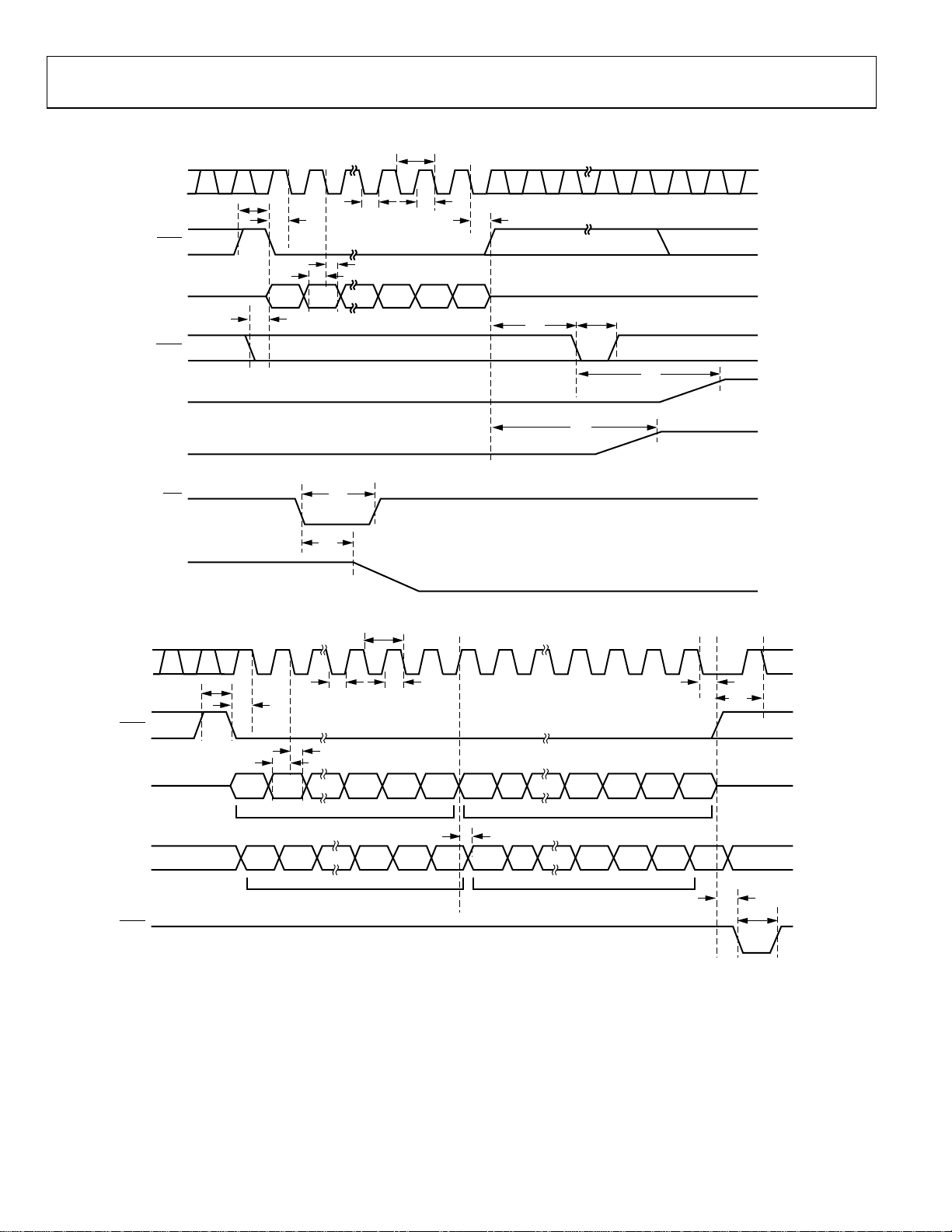
Figure 2. Serial Interface Timing Diagram
t
1
SCLK
SYNC
SDIN
SDO
LDAC
8442
t
17
t
4
t
7
t
3
t
8
t
2
INPUT WORD FOR DAC N – 1INPUT WORD FOR DAC N
t
16
DB23
INPUT WORD FOR DAC NUNDEFINED
t
5
t
15
D0BD32BD0BD32B
DB0
t
10
t
11
06468-003
Figure 3. Daisy-Chain Timing Diagram
Rev. F | Page 6 of 31
Page 7
Data Sheet AD5724/AD5734/AD5754
SCLK
SYNC
1
24 24
t
1
17
SDIN
SDO
DB23 DB0 DB23 DB0
REGIST ER TO BE RE AD
DB23 DB0 DB23 DB0
UNDEFINED
NOP CONDI TIONINPUT WORD SPECIFIES
SELECTED REGISTER DATA
CLOCKED O UT
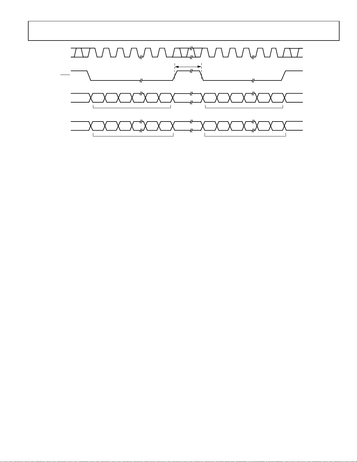
Figure 4. Readback Timing Diagram
06468-004
Rev. F | Page 7 of 31
Page 8
AD5724/AD5734/AD5754 Data Sheet
(whichever is less)
Digital Outputs to GND
−0.3 V to DVCC + 0.3 V or 7 V
Operating Temperature Range, TA
ABSOLUTE MAXIMUM RATINGS
TA = 25°C, unless otherwise noted. Transient currents of up to
100 mA do not cause SCR latch-up.
Table 4.
Parameter Rating
AVDD to GND −0.3 V to +17 V
AVSS to GND +0.3 V to −17 V
DVCC to GND −0.3 V to +7 V
Digital Inputs to GND −0.3 V to DVCC + 0.3 V or 7 V
(whichever is less)
REFIN to GND −0.3 V to +5 V
V
A, V
B, V
C, V
OUT
OUT
OUT
DAC_GND to GND −0.3 V to +0.3 V
SIG_GND to GND −0.3 V to +0.3 V
Industrial −40°C to +85°C
Storage Temperature Range −65°C to +150°C
Junction Temperature, TJ max 150°C
24-Lead TSSOP Package
θJA Thermal Impedance 42°C/W
θJC Thermal Impedance 9°C/W
Power Dissipation (TJ max − TA)/ θJA
Lead Temperature JEDEC industry standard
Soldering J-STD-020
ESD (Human Body Model) 3.5 kV
D to GND AVSS to AVDD
OUT
Stresses at or above those listed under Absolute Maximum
Ratings may cause permanent damage to the product. This is a
stress rating only; functional operation of the product at these
or any other conditions above those indicated in the operational
section of this specification is not implied. Operation beyond
the maximum operating conditions for extended periods may
affect product reliability.
ESD CAUTION
Rev. F | Page 8 of 31
Page 9
Data Sheet AD5724/AD5734/AD5754
06468-005
24
23
22
21
20
19
18
17
16
15
14
13
1
2
3
4
5
6
7
8
9
10
11
12
AD5724/
AD5734/
AD5754
CLR
LDAC
AV
SS
NC
V
OUT
A
V
OUT
B
SYNC
NC
BIN/2sCOMP
GND
SDO
REFIN
SIG_GND
SCLK
SDIN
NC
AV
DD
V
OUT
C
V
OUT
D
SIG_GND
DAC_GND
DAC_GND
DV
CC
NC
TOP VIEW
(Not to S cale)
NOTES
1. NC = NO CONNE CT.
2. IT IS RECOMMENDED THAT THE EXPOSED PAD BE
THERMALL Y CONNECTED TO A COPPER PL ANE
FOR ENHANCED THE RM AL PERFORM ANCE .
Load DAC, Logic Input. This is used to update the DAC registers and consequently, the analog outputs. When
held high during the write cycle, the DAC input register is updated, but the output update is held off until the
External Reference Voltage Input. Reference input range is 2 V to 3 V. REFIN = 2.5 V for specified performance.
PIN CONFIGURATION AND FUNCTION DESCRIPTIONS
Figure 5. Pin Configuration
Table 5. Pin Function Descriptions
Pin No. Mnemonic Description
1 AVSS Negative Analog Supply. Voltage ranges from −4.5 V to −16.5 V. This pin can connect to 0 V if output ranges
are unipolar.
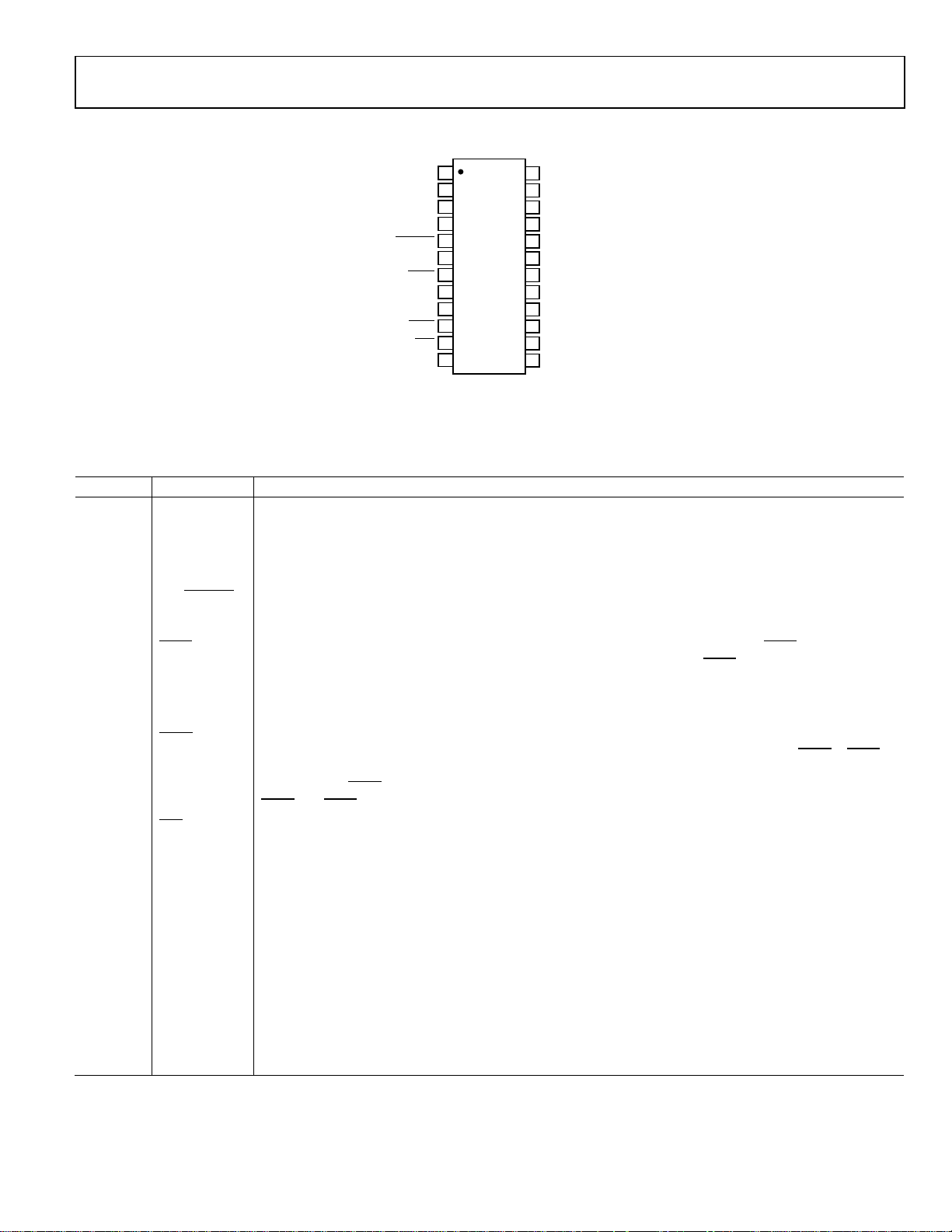
2, 6, 12, 13 NC No connect. Do not connect to these pins.
3 V
4 V
5 BIN/
A Analog Output Voltage of DAC A. The output amplifier is capable of directly driving a 2 kΩ, 4000 pF load.
OUT
B Analog Output Voltage of DAC B. The output amplifier is capable of directly driving a 2 kΩ, 4000 pF load.
OUT
2sCOMP
Determines the DAC coding for a bipolar output range. This pin must be hardwired to either DVCC or GND.
When hardwired to DVCC, input coding is offset binary. When hardwired to GND, input coding is twos
complement. (For unipolar output ranges, coding is always straight binary).
7
Active Low Input. This is the frame synchronization signal for the serial interface. While
SYNC
transferred on the falling edge of SCLK. Data is latched on the rising edge of
8 SCLK Serial Clock Input. Data is clocked into the shift register on the falling edge of SCLK. This operates at clock
speeds up to 30 MHz.
9 SDIN Serial Data Input. Data must be valid on the falling edge of SCLK.
10
LDAC
this pin is tied permanently low, the addressed DAC register is updated on the rising edge of
11
falling edge of
. The
LDAC
Active Low Input. Asserting this pin sets the DAC registers to zero-scale code or midscale code (user-selectable).
CLR
LDAC
. In this mode, all analog outputs can be updated simultaneously on the falling edge of
LDAC
pin must not be left unconnected.
14 DVCC Digital Supply. Voltage ranges from 2.7 V to 5.5 V.
15 GND Ground Reference.
16 SDO Serial Data Output. Used to clock data from the serial register in daisy-chain or readback mode. Data is
clocked out on the rising edge of SCLK and is valid on the falling edge of SCLK.
17 REFIN
18, 19 DAC_GND Ground Reference for the Four Digital-to-Analog Converters.
20, 21 SIG_GND Ground Reference for the Four Output Amplifiers.
22 V
23 V
24 AVDD Positive Analog Supply. Voltage ranges from 4.5 V to 16.5 V.
Exposed
Paddle
D Analog Output Voltage of DAC D. The output amplifier is capable of directly driving a 2 kΩ, 4000 pF load.
OUT
C Analog Output Voltage of DAC C. The output amplifier is capable of directly driving a 2 kΩ, 4000 pF load.
OUT
AVSS This exposed paddle can be connected to the potential of the AVSS pin, or alternatively, it can be left electrically
unconnected. It is recommended that the paddle be thermally connected to a copper plane for enhanced thermal
performance.
Rev. F | Page 9 of 31
is low, data is
SYNC
.
SYNC
SYNC
. If
LDAC
is
Page 10
AD5724/AD5734/AD5754 Data Sheet
CODE
INL ERROR (LSB)
0 10,000
20,000 30,000
40,000
50,000 60,000
–8
–6
–4
–2
0
2
4
6
AVDD/AV
SS
= +12V/0V, RANGE = +10V
AV
DD
/AV
SS
= ±12V, RANGE = ±10V
AV
DD
/AV
SS
= ±6.5V, RANG E = ±5V
AV
DD
/AV
SS
= +6.5V/0V, RANGE = +5V
06468-013
–2.0
–1.5
–1.0
–0.5
0
0.5
1.0
1.5
CODE
INL ERROR (LSB)
AV
DD
/AVSS = +12V/0V, RANGE = +10V
AVDD/AVSS = ±12V, RANGE = ±10V
AVDD/AVSS = ±6.5V, RANG E = ±5V
AVDD/AVSS = +6.5V/0V, RANGE = +5V
0 2000 4000
6000 8000 10,000 12,000 14,000 16,000
06468-014
–0.5
–0.4
–0.3
–0.2
–0.1
0
0.1
0.2
0.3
0 500 1000 1500 2000 2500 3000 3500 4000
CODE
INL ERROR (LSB)
AVDD/AVSS = +12V/0V, RANGE = +10V
AV
DD
/AVSS = ±12V, RANGE = ±10V
AVDD/AVSS = ±6.5V, RANG E = ±5V
AVDD/AVSS = +6.5V/0V, RANGE = +5V
06468-015
CODE
DNL ERROR (LS B)
AVDD/AVSS = +12V/0V, RANGE = +10V
AVDD/AVSS = ±12V, RANGE = ±10V
AV
DD
/AVSS = ±6.5V, RANG E = ±5V
AVDD/AVSS = +6.5V/0V, RANGE = +5V
0 10,000 20,000 30,000 40000 50,000 60,000
–0.8
–0.6
–0.4
–0.2
0
0.2
0.4
0.6
06468-016
–0.20
–0.15
–0.10
–0.05
0
0.05
0.10
0.15
CODE
DNL ERROR (L S B)
AV
DD
/AVSS = +12V/0V, RANGE = +10V
AVDD/AV
SS
= ±12V, RANGE = ±10V
AVDD/AVSS = ±6.5V, RANG E = ±5V
AV
DD
/AVSS = +6.5V/0V, RANGE = +5V
0 2000 4000 6000
8000 10000 12000 14000 16000
06468-017
–0.05
–0.04
–0.03
–0.02
–0.01
0
0.01
0.02
0.03
0.04
0 500 1000 1500
2000 2500 3000 3500 4000
AVDD/AVSS = +12V/0V, RANGE = +10V
AVDD/AVSS = ±12V, RANGE = ±10V
AV
DD
/AVSS = ±6.5V, RANG E = ±5V
AVDD/AV
SS
= +6.5V/0V, RANGE = +5V
CODE
DNL ERROR (L S B)
06468-018
TYPICAL PERFORMANCE CHARACTERISTICS
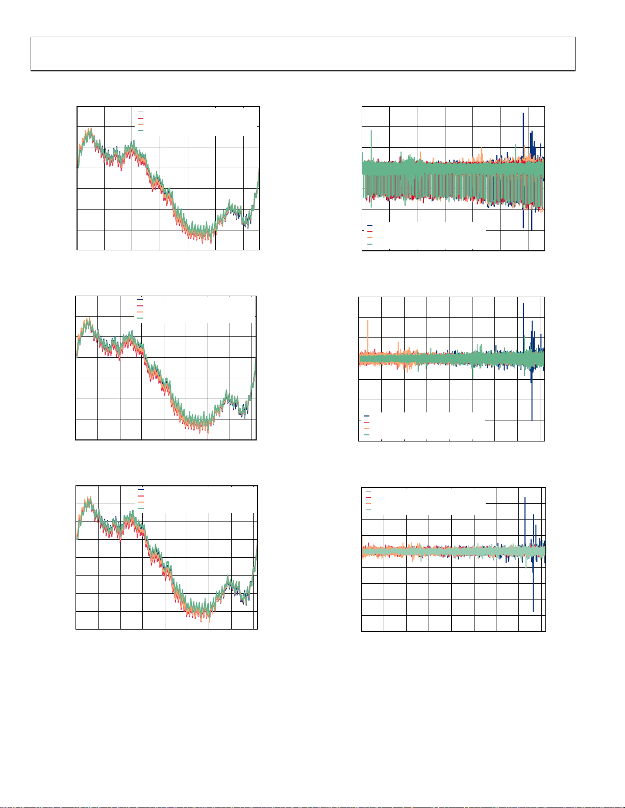
Figure 6. AD5754 INL Error vs. Code
Figure 7. AD5734 INL Error vs. Code
Figure 9. AD5754 DNL Error vs. Code
Figure 10. AD5734 DNL Error vs. Code
Figure 8. AD5724 INL Error vs. Code
Figure 11. AD5724 DNL Error vs. Code
Rev. F | Page 10 of 31
Page 11
Data Sheet AD5724/AD5734/AD5754
TEMPERATURE (°C)
INL ERROR ( LSB)
–8
–6
–4
–2
0
2
4
6
8
–40 –20 0 20 40 60 80
MAX INL ±10V
MAX INL ±5V
MIN INL ±10V
MIN INL ±5V
MAX INL +10V
MIN INL +10V
MAX INL +5V
MIN INL +5V
06468-044
–0.6
–0.5
–0.4
–0.3
–0.2
–0.1
0
0.1
TEMPERATURE (°C)
DNL ERROR (L S B)
–40 –20 0 20 40 60 80
MAX DNL ±10V
MAX DNL ±5V
MIN DNL ±10V
MIN DNL ±5V
MAX DNL +10V
MIN DNL +10V
MAX DNL +5V
MIN DNL +5V
06468-045
–10
–8
–6
–4
–2
0
2
4
6
8
10
SUPPLY (V)
INL ERROR ( LSB)
11.5 12.512.0 13.5 14.013.0 14.5 15.0 15.5 16.0 16.5
BIPOLAR 10V M IN
UNIPOLAR 10V M IN
BIPOLAR 10V M AX
UNIPOLAR 10V M AX
06468-034
SUPPLY VOLTAGE (V)
5.5 8.56.5 7.5 10.5 11.59.5 12.5 13.5 14.5 15.5 16.5
–10
–8
–6
–4
–2
0
2
4
6
8
10
INL ERROR ( LSB)
BIPOLAR 5V M IN
UNIPOLAR 5V M IN
BIPOLAR 5V M AX
UNIPOLAR 5V M AX
06468-035
SUPPLY VOLTAGE (V)
DNL ERROR (L S B)
11.5 12.512.0 13.5 14.013.0 14.5 15.0 15.5 16.0 16.5
0
0.6
0.4
0.2
1.0
0.8
–0.6
–0.4
–0.2
–1.0
–0.8
BIPOLAR 10V M IN
UNIPOLAR 10V M IN
BIPOLAR 10V M AX
UNIPOLAR 10V M AX
06468-032
SUPPLY VOLTAGE (V)
DNL ERROR (L S B)
5.5 8.56.5 7.5 10.5 11.59.5 12.5 13.5 14.5 15.5 16.5
0
0.6
0.4
0.2
1.0
0.8
–0.6
–0.4
–0.2
–1.0
–0.8
BIPOLAR 5V M IN
UNIPOLAR 5V M IN
BIPOLAR 5V M AX
UNIPOLAR 5V M AX
06468-033
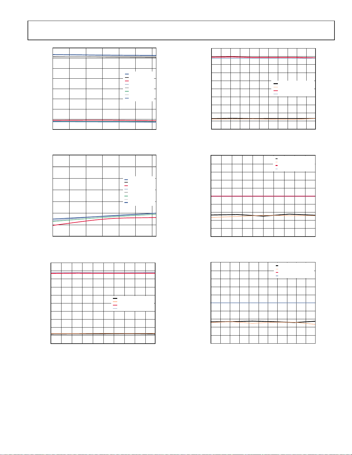
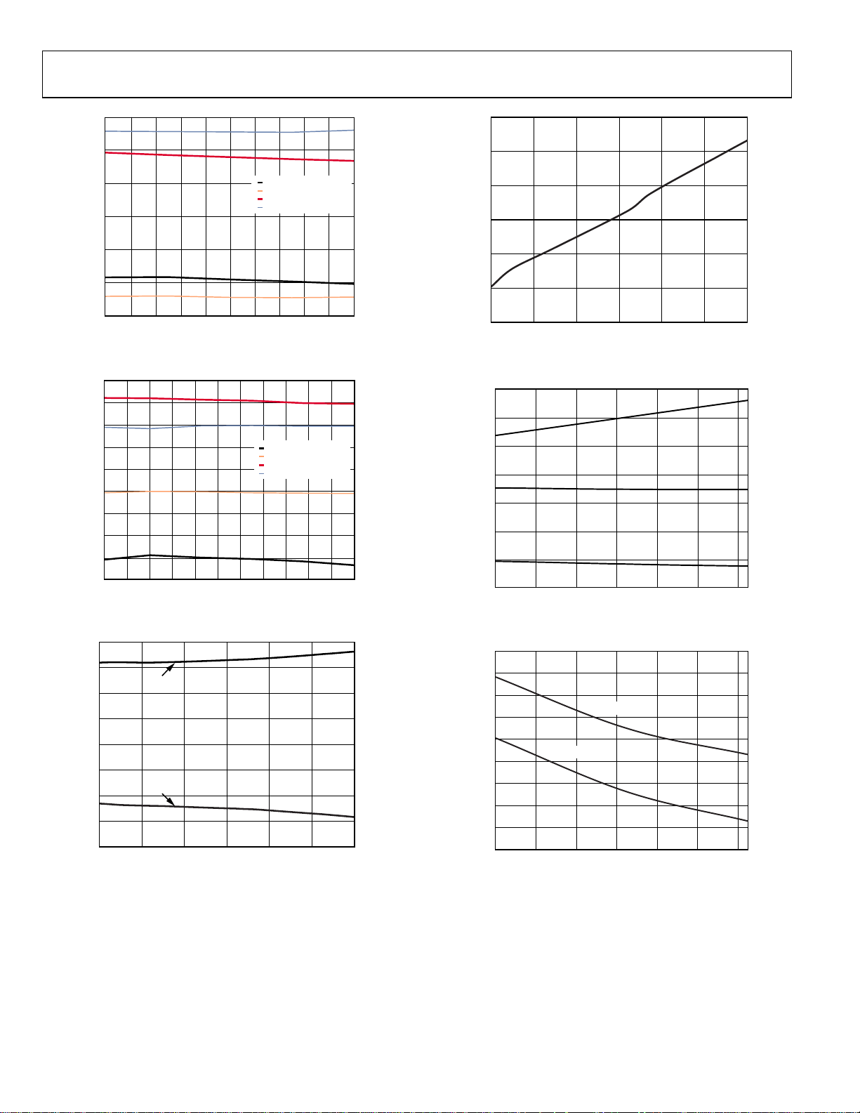
Figure 12. AD5754 INL Error vs. Temperature
Figure 13. AD5754 DNL Error vs. Temperature
Figure 15. AD5754 INL Error vs. Supply Voltage
Figure 16. AD5754 DNL Error vs. Supply Voltage
Figure 14. AD5754 INL Error vs. Supply Voltage
Figure 17. AD5754 DNL Error vs. Supply Voltage
Rev. F | Page 11 of 31
Page 12
AD5724/AD5734/AD5754 Data Sheet
SUPPLY VOLTAGE (V)
11.5 12.512.0 13.5
14.013.0 14.5
15.0
15.5 16.0
16.5
BIPOLAR 10V M IN
UNIPOLAR 10V M IN
BIPOLAR 10V M AX
UNIPOLAR 10V M AX
TUE (%)
–0.04
–0.03
–0.02
–0.01
0
0.01
0.02
06468-036
SUPPLY VOLTAGE (V)
5.5 8.56.5 7.5 10.5 11.59.5 12.5 13.5 14.5 15.5 16.5
–0.05
–0.04
–0.03
–0.02
–0.01
0
0.01
0.02
0.03
0.04
TUE (%)
BIPOLAR 5V M IN
UNIPOLAR 5V M IN
BIPOLAR 5V M AX
UNIPOLAR 5V M AX
06468-037
–8
–6
–4
–2
0
2
4
6
8
4.5 6.5 8.5 10.5 12.5 14.5 16.5
I
DD
(mA)
I
SS
(mA)
AV
DD
/AVSS (V)
AI
DD
/AI
SS
(mA)
06468-038
AV
DD
(V)
AI
DD
(mA)
4
5
6
7
8
9
10
4.5 6.5 8.5 10.5 12.5 14.5 16.5
06468-042
–3
–2
–1
0
1
2
3
4
TEMPERATURE (°
C)
ZERO-SCALE ERROR (mV)
–40 –20
0 20 40
60 80
±10V
±5V
+10V
06468-046
–1.0
–0.8
–0.6
–0.4
–0.2
0
0.2
0.4
0.6
0.8
TEMPERATURE (
°C)
BIPOLAR ZERO ERROR (mV )
–40 –20
0 20 40 60
80
±5V RANGE
±10V RANGE
06468-047
Figure 18. AD5754 TUE vs. Supply Voltage
Figure 19. AD5754 TUE vs. Supply Voltage
Figure 21. Supply Current vs. Supply Voltage (Single Supply)
Figure 22. Zero-Scale Error vs. Temperature
Figure 20. Supply Current vs. Supply Voltage (Dual Supply)
Figure 23. Bipolar Zero Error vs. Temperature
Rev. F | Page 12 of 31
Page 13
Data Sheet AD5724/AD5734/AD5754
–0.06
–0.04
–0.02
0
0.02
0.04
0.06
±10V
±5V
+10V
TEMPERATURE (
°C)
GAIN ERROR ( % FSR)
–40 –20 0 20 40 60 80
06468-048
V
LOGIC
(V)
DI
CC
(µA)
–100
0
100
200
300
400
500
600
700
800
900
1000
0 1 2 3 4
5 6
DV
CC
= 5V
DV
CC
= 3V
06468-043
OUTPUT CURRENT (mA)
OUTPUT VOLTAGE DELTA (V)
–0.020
–0.015
–0.010
–0.005
0
0.005
0.010
–25 –20 –15 –10 –5 0 5 10 15 20 25
±5V RANGE, CO DE = 0xFFFF
±10V RANGE, CO DE = 0xFFFF
+10V RANGE, CO DE = 0xFFFF
+5V RANGE, CO DE = 0xFFFF
±5V RANGE, CO DE = 0x0000
±10V RANGE, CO DE = 0x0000
06468-040
–15
–10
–5
0
5
10
15
–3
–1 1 3 5 7 9 11
TIME (µs)
OUTPUT VOLTAGE (V)
06468-022
–7
–5
–3
–1
1
3
5
7
–3 –1
1 3 5
7 9 11
TIME (µs)
OUTPUT VOLTAGE (V)
06468-023
0
2
4
6
8
10
12
–3 –1 1 3 5 7 9
11
TIME (µs)
OUTPUT VOLTAGE (V)
06468-024
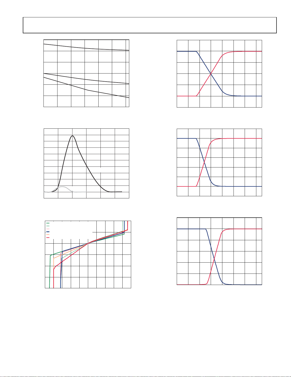
Figure 24. Gain Error vs. Temperature
Figure 25. Digital Current vs. Logic Input Voltage
Figure 27. Full-Scale Settling Time, ±10 V Range
Figure 28. Full-Scale Settling Time, ±5 V Range
Figure 26. Output Source and Sink Capability
Figure 29. Full-Scale Settling Time, 10 V Range
Rev. F | Page 13 of 31
Page 14
AD5724/AD5734/AD5754 Data Sheet
6
5
4
3
2
OUTPUT VOLTAGE (V)
1
0
–3 –1 1 3 5 7 9 11
TIME (µs)
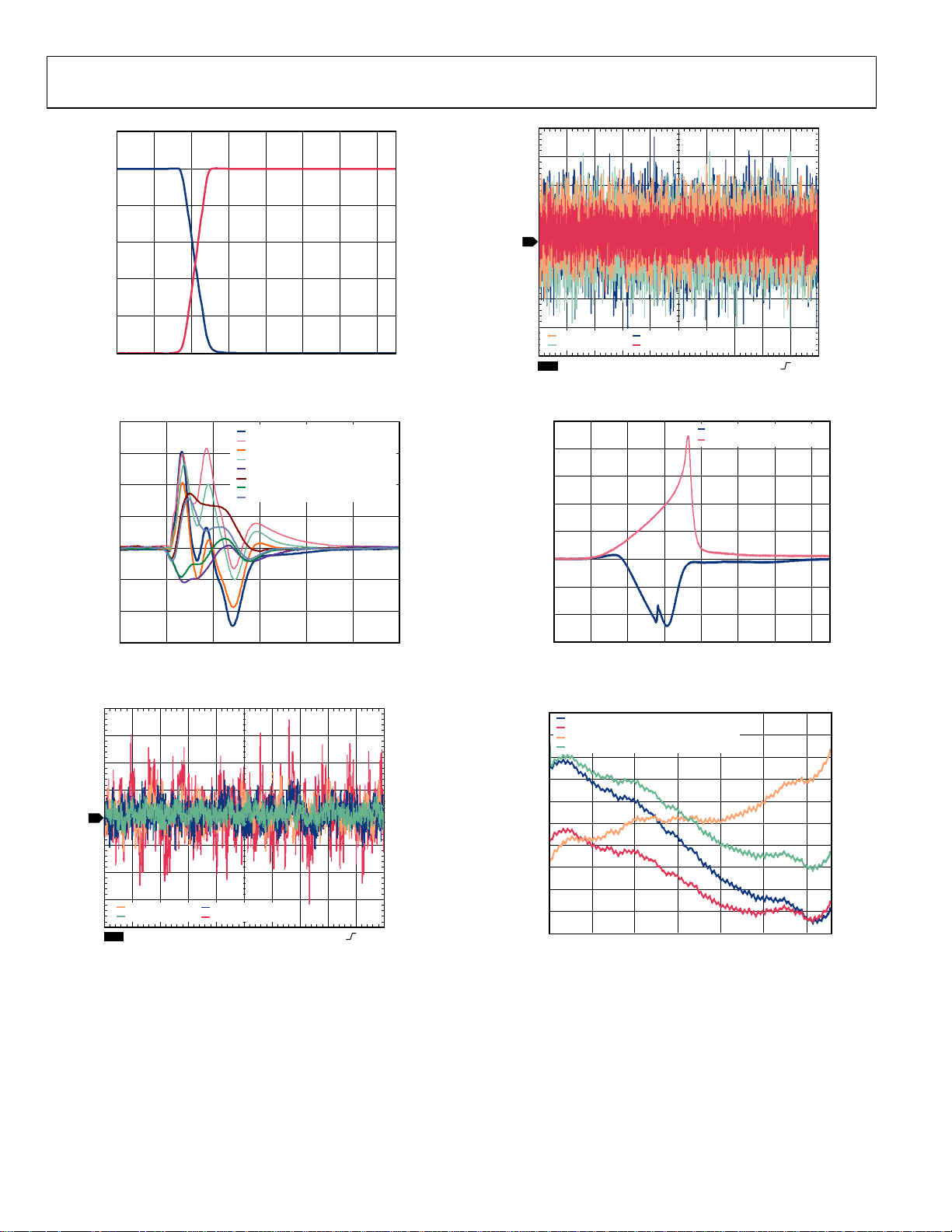
Figure 30. Full-Scale Settling Time, +5 V Range
–0.005
OUTPUT VOLTAGE (V)
–0.010
0.020
0.015
0.010
0.005
0
±10V RANGE, 0x7F FF TO 0x8000
±10V RANGE, 0x8000 T O 0x7FFF
±5V RANGE, 0x7F FF TO 0x8000
±5V RANGE, 0x8000 T O 0x7FFF
+10V RANGE, 0x7F FF TO 0x8000
+10V RANGE, 0x8000 T O 0x7FFF
+5V RANGE, 0x7F FF TO 0x8000
+5V RANGE, 0x8000 T O 0x7FFF
6468-025
±
±
1
RANGE = ±5V
RANGE = +5V
RANGE = +10V
RANGE = ±10V
CH1 5µV M5s LINE 73.8V
Figure 33. Peak-to-Peak Noise, 100 kHz Bandwidth
OUTPUT VOLTAGE (V)
0.10
0.08
0.06
0.04
0.02
0
–0.02
–0.04
AVDD/AVSS = ±16.5V
= +16.5V, AVSS = 0V
AV
DD
06468-027
–0.015
–1012345
TIME (µs)
Figure 31. Digital-to-Analog Glitch Energy
1
RANGE = ±5V
RANGE = +5V
CH1 5µV M 5s LINE 73.8V
RANGE = +10V
RANGE = ±10V
Figure 32. Peak-to-Peak Noise, 0.1 Hz to 10 Hz Bandwidth
–0.06
–50–30–101030507090
06468-039
TIME (µs)
06468-041
Figure 34. Output Glitch on Power-Up
15
AVDD/AVSS = +12V/0V, RANGE = +10V
/AVSS = ±12V, RANGE = ±10V
AV
DD
10
5
0
–5
–10
TUE (LSB)
–15
–20
–25
–30
6468-026
–35
/AVSS = ±6.5V, RA NGE = ±5V
AV
DD
/AVSS = +6.5V/0V, RANGE = +5V
AV
DD
0 1000 2000 3000 4000 5000 6000
CODE
06468-019
Figure 35. AD5754 TUE vs. Code
Rev. F | Page 14 of 31
Page 15
Data Sheet AD5724/AD5734/AD5754
–10
–8
–6
–4
–2
0
2
4
0
2000 4000 6000 8000 10,000 12,000 14,000 16,000
CODE
TUE (LSB)
AV
DD
/AV
SS
= +12V/0V, RANGE = +10V
AV
DD
/AV
SS
= ±12V, RANGE = ±10V
AV
DD
/AV
SS
= ±6.5V, RANG E = ±5V
AV
DD
/AV
SS
= +6.5V/0V, RANGE = +5V
06468-020
–2.5
–2.0
–1.5
–1.0
–0.5
0
0.5
1.0
0 500
1000 1500 2000 2500 3000 3500 4000
CODE
TUE (LSB)
AVDD/AVSS = +12V/0V, RANGE = +10V
AV
DD
/AVSS = ±12V, RANGE = ±10V
AV
DD
/AV
SS
= ±6.5V, RANG E = ±5V
AVDD/AVSS = +6.5V/0V, RANGE = +5V
06468-021
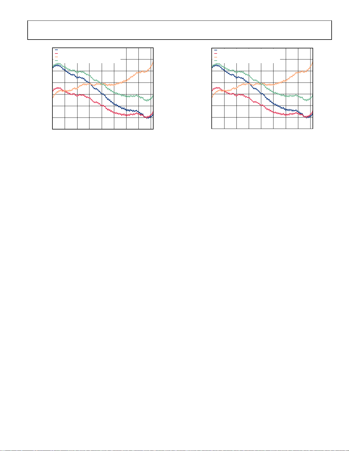
Figure 36. AD5734 TUE vs. Code
Figure 37. AD5724 TUE vs. Code
Rev. F | Page 15 of 31
Page 16

AD5724/AD5734/AD5754 Data Sheet
TERMINOLOGY
Relative Accuracy or Integral Nonlinearity (INL)
For the DAC, relative accuracy, or integral nonlinearity, is a
measure of the maximum deviation in LSBs from a straight line
passing through the endpoints of the DAC transfer function. A
typical INL vs. code plot can be seen in Figure 6.
Differential Nonlinearity (DNL)
Differential nonlinearity is the difference between the measured
change and the ideal 1 LSB change between any two adjacent
codes. A specified differential nonlinearity of ±1 LSB maximum
ensures monotonicity. This DAC is guaranteed monotonic by
design. A typical DNL vs. code plot can be seen in Figure 9.
Monotonicity
A DAC is monotonic if the output either increases or remains
constant for increasing digital input code. The AD5724/AD5734/
AD5754 are monotonic over the full operating temperature
range of the devices.
Bipolar Zero Error
Bipolar zero error is the deviation of the analog output from the
ideal half-scale output of 0 V when the DAC register is loaded
with 0x8000 (straight binary coding) or 0x0000 (twos complement
coding). A plot of bipolar zero error vs. temperature can be seen
in Figure 23.
Bipolar Zero Temperature Coefficient (TC)
Bipolar zero TC is a measure of the change in the bipolar zero
error with a change in temperature. It is expressed in ppm FSR/°C.
Zero-Scale Error or Negative Full-Scale Error
Zero-scale error is the error in the DAC output voltage when
0x0000 (straight binary coding) or 0x8000 (twos complement
coding) is loaded to the DAC register. Ideally, the output voltage
must be negative full-scale −1 LSB. A plot of zero-scale error vs.
temperature can be seen in Figure 22.
Zero-Scale TC
Zero-scale TC is a measure of the change in zero-scale error with a
change in temperature. Zero-scale TC is expressed in ppm FSR/°C.
Output Voltage Settling Time
Output voltage settling time is the amount of time required for
the output to settle to a specified level for a full-scale input change.
A plot for full-scale settling time can be seen in Figure 27.
Slew Rate
The slew rate of a device is a limitation in the rate of change of
the output voltage. The output slewing speed of a voltage output
DAC is usually limited by the slew rate of the amplifier used at
the output. Slew rate is measured from 10% to 90% of the
output signal and is given in V/µs.
Gain Error
Gain error is a measure of the span error of the DAC. It is the
deviation in slope of the DAC transfer characteristic from
the ideal and is expressed in % FSR. A plot of gain error vs.
temperature can be seen in Figure 24.
Gain TC
Gain TC is a measure of the change in gain error with changes
in temperature. Gain TC is expressed in ppm FSR/°C.
Total Unadjusted Error (TUE)
Total unadjusted error is a measure of the output error taking
all the various errors into account, namely INL error, offset
error, gain error, and output drift over supplies, temperature,
and time. TUE is expressed in % FSR.
Digital-to-Analog Glitch Impulse
Digital-to-analog glitch impulse is the impulse injected into the
analog output when the input code in the DAC register changes
state, but the output voltage remains constant. It is normally
specified as the area of the glitch in nV-sec and is measured
when the digital input code is changed by 1 LSB at the major
carry transition (0x7FFF to 0x8000). See Figure 31.
Glitch Impulse Peak Amplitude
Glitch impulse peak amplitude is the peak amplitude of the
impulse injected into the analog output when the input code in
the DAC register changes state. It is specified as the amplitude
of the glitch in mV and is measured when the digital input code
is changed by 1 LSB at the major carry transition (0x7FFF to
0x8000). See Figure 31.
Digital Feedthrough
Digital feedthrough is a measure of the impulse injected into
the analog output of the DAC from the digital inputs of the
DAC, but is measured when the DAC output is not updated.
It is specified in nV-sec and measured with a full-scale code
change on the data bus.
Power Supply Sensitivity
Power supply sensitivity indicates how the output of the DAC is
affected by changes in the power supply voltage. It is measured
by superimposing a 50 Hz/60 Hz, 200 mV p-p sine wave on the
supply voltages and measuring the proportion of the sine wave
that transfers to the outputs.
Rev. F | Page 16 of 31
Page 17

Data Sheet AD5724/AD5734/AD5754
DC Crosstalk
This is the dc change in the output level of one DAC in response
to a change in the output of another DAC. It is measured with a
full-scale output change on one DAC while monitoring another
DAC. It is expressed in LSBs.
Digital Crosstalk
Digital crosstalk is a measure of the impulse injected into the
analog output of one DAC from the digital inputs of another
DAC, but is measured when the DAC output is not updated.
It is specified in nV-sec and measured with a full-scale code
change on the data bus.
DAC-to-DAC Crosstalk
DAC-to-DAC crosstalk is the glitch impulse transferred to the
output of one DAC due to a digital code change and a subsequent
output change of another DAC. This includes both digital and
analog crosstalk. It is measured by loading one of the DACs
with a full-scale code change (all 0s to all 1s and vice versa) with
LDAC
low and monitoring the output of another DAC. The
energy of the glitch is expressed in nV-sec.
Rev. F | Page 17 of 31
Page 18
GND
RESISTOR
STRING
REF (+)
REF (–)
CONFIGURABLE
OUTPUT
AMPLIFIER
OUTPUT
RANGE CONTROL
06468-006
REFIN
DAC REGIST E R
V
OUT
x
R
R
R
R
R
TO OUTPUT
AMPLIFIER
REFIN
06468-007
AD5724/AD5734/AD5754 Data Sheet
THEORY OF OPERATION
The AD5724/AD5734/AD5754 are quad, 12-/14-/16-bit, serial
input, unipolar/bipolar, voltage output DACs. They operate from
unipolar supply voltages of +4.5 V to +16.5 V or bipolar supply
voltages of ±4.5 V to ±16.5 V. In addition, the devices have
software-selectable output ranges of +5 V, + 10 V, +10.8 V, ± 5 V,
±10 V, and ±10.8 V. Data is written to the AD5724/AD5734/
AD5754 in a 24-bit word format via a 3-wire serial interface.
The devices also offer an SDO pin to facilitate daisy-chaining
or readback.
The AD5724/AD5734/AD5754 incorporate a power-on reset
circuit to ensure that the DAC registers power up loaded with
0x0000. When powered on, the outputs are clamped to 0 V via
a low impedance path.
ARCHITECTURE
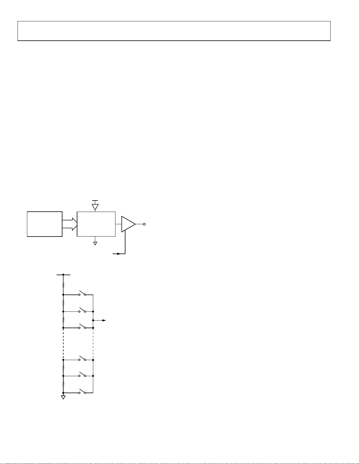
The DAC architecture consists of a string DAC followed by an
output amplifier. Figure 38 shows a block diagram of the DAC
architecture. The reference input is buffered before being
applied to the DAC.
Figure 38. DAC Architecture Block Diagram
The resistor string structure is shown in Figure 39. It is a string
of resistors, each of value R. The code loaded to the DAC
register determines the node on the string where the voltage is
to be tapped off and fed into the output amplifier. The voltage is
tapped off by closing one of the switches connecting the string
to the amplifier. Because it is a string of resistors, it is
guaranteed monotonic.
Output Amplifiers
The output amplifiers are capable of generating both unipolar
and bipolar output voltages. They are capable of driving a load
of 2 kΩ in parallel with 4000 pF to GND. The source and sink
capabilities of the output amplifiers can be seen in Figure 26.
The slew rate is 3.5 V/µs with a full-scale settling time of 10 µs.
Reference Buffers
The AD5724/AD5734/AD5754 require an external reference
source. The reference input has an input range of 2 V to 3 V,
with 2.5 V for specified performance. This input voltage is then
buffered before it is applied to the DAC cores.
POWER-UP SEQUENCE
Because the DAC output voltage is controlled by the voltage
monitor and control block (see Figure 42), it is important to
power the DV
and AV
SS
pin before applying any voltage to the AVDD
CC
pins; otherwise, the G1 and G2 transmission gates are at
an undefined state. The ideal power-up sequence is in the
following order: GND, SIG_GND, DAC_GND, DV
AV
, and then the digital inputs. The relative order of powering
SS
AV
and AVSS is not important, provided that they are powered
DD
up after DV
.
CC
, AVDD,
CC
SERIAL INTERFACE
The AD5724/AD5734/AD5754 are controlled over a versatile
3-wire serial interface that operates at clock rates up to 30 MHz.
It is compatible with SPI, QSPI™, MICROWIRE™, and DSP
standards.
Input Shift Register
The input shift register is 24 bits wide. Data is loaded into the
device MSB first as a 24-bit word under the control of a serial
clock input, SCLK. The input register consists of a read/write
bit, three register select bits, three DAC address bits, and 16 data
bits. The timing diagram for this operation is shown in Figure 2.
Figure 39. Resistor String Structure
Rev. F | Page 18 of 31
Page 19
*
ADDITIONAL PINS OMITTED FOR CLARITY.
68HC11
*
MISO
SDIN
SCLK
MOSI
SCK
PC7
PC6
SDO
SCLK
SDO
SCLK
SDO
SDIN
SDIN
SYNC
SYNC
SYNC
LDAC
LDAC
LDAC
AD5724/
AD5734/
AD5754*
AD5724/
AD5734/
AD5754*
AD5724/
AD5734/
AD5754*
06468-008
Data Sheet AD5724/AD5734/AD5754
Standalone Operation
The serial interface works with both a continuous and noncontinuous serial clock. A continuous SCLK source can be used
SYNC
only if
is held low for the correct number of clock cycles.
In gated clock mode, a burst clock containing the exact number
SYNC
of clock cycles must be used and
must be taken high after
the final clock to latch the data. The first falling edge of
starts the write cycle. Exactly 24 falling clock edges must be
SYNC
applied to SCLK before
brought high before the 24
is brought high again. If
th
falling SCLK edge, the data written
is invalid. If more than 24 falling SCLK edges are applied before
SYNC
is brought high, the input data is also invalid. The input
register addressed is updated on the rising edge of
SYNC
another serial transfer to take place,
must be brought low
SYNC
again. After the end of the serial data transfer, data is
automatically transferred from the input shift register to the
addressed register.
When the data has been transferred into the chosen register of
the addressed DAC, all DAC registers and outputs can be
updated by taking
LDAC
low while
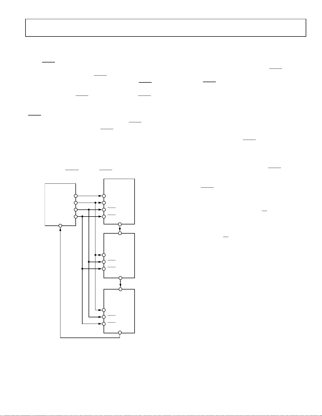
Figure 40. Daisy Chaining the AD5724/AD5734/AD5754
SYNC
is high.
SYNC
SYNC
. For
is
Daisy-Chain Operation
For systems that contain several devices, the SDO pin can be
used to daisy-chain several devices together. Daisy-chain mode
can be useful in system diagnostics and in reducing the number
of serial interface lines. The first falling edge of
SYNC
starts the
write cycle. SCLK is continuously applied to the input shift
SYNC
register when
is low. If more than 24 clock pulses are
applied, the data ripples out of the shift register and appears on
the SDO line. This data is clocked out on the rising edge of
SCLK and is valid on the falling edge. By connecting the SDO
of the first device to the SDIN input of the next device in the
chain, a multidevice interface is constructed. Each device in the
system requires 24 clock pulses. Therefore, the total number of
clock cycles must equal 24 × N, where N is the total number of
AD5724/AD5734/AD5754 devices in the chain. When the serial
SYNC
transfer to all devices is complete,
is taken high. This
latches the input data in each device in the daisy chain and
prevents any further data from being clocked into the input shift
register. The serial clock can be a continuous or a gated clock.
A continuous SCLK source can only be used if
SYNC
is held
low for the correct number of clock cycles. In gated clock mode,
a burst clock containing the exact number of clock cycles must
be used, and
SYNC
must be taken high after the final clock to
latch the data.
Readback Operation
Readback mode is invoked by setting the R/W bit = 1 in the
serial input shift register write. (If the SDO output is disabled
via the SDO disable bit in the control register, it is automatically
enabled for the duration of the read operation, after which it is
disabled again). With R/
W
= 1, Bit A2 to Bit A0 in association
with Bit REG2 to Bit REG0, select the register to be read. The
remaining data bits in the write sequence are don’t care bits.
During the next SPI write, the data appearing on the SDO output
contains the data from the previously addressed register. For a
read of a single register, the NOP command can clock out the
data from the selected register on SDO. The readback diagram
in
Figure 4 shows the readback sequence. For example, to read
back the DAC register of Channel A, the following sequence
must be implemented:
1. Write 0x800000 to the AD5724/AD5734/AD5754 input
register. This configures the device for read mode with the
DAC register of Channel A selected. Note that all the data
bits, DB15 to DB0, are don’t care bits.
2. Follow this with a second write, a NOP condition, 0x180000.
During this write, the data from the register is clocked out
on the SDO line.
Rev. F | Page 19 of 31
Page 20
SYNC
SCLK
V
OUT
DAC
REGISTER
INTERFACE
LOGIC
OUTPUT
AMPLIFIER
LDAC
SDO
SDIN
REFIN
INPUT
REGISTER
12-/14-/16-BIT
DAC
06468-009
×=
N
REFIN
OUT
D
GainVV
2
22
REFIN
N
REFIN
OUT
VGain
D
GainVV
×
−
×
=
±10.8
8.64
AD5724/AD5734/AD5754 Data Sheet
LOAD DAC (
LDAC
)
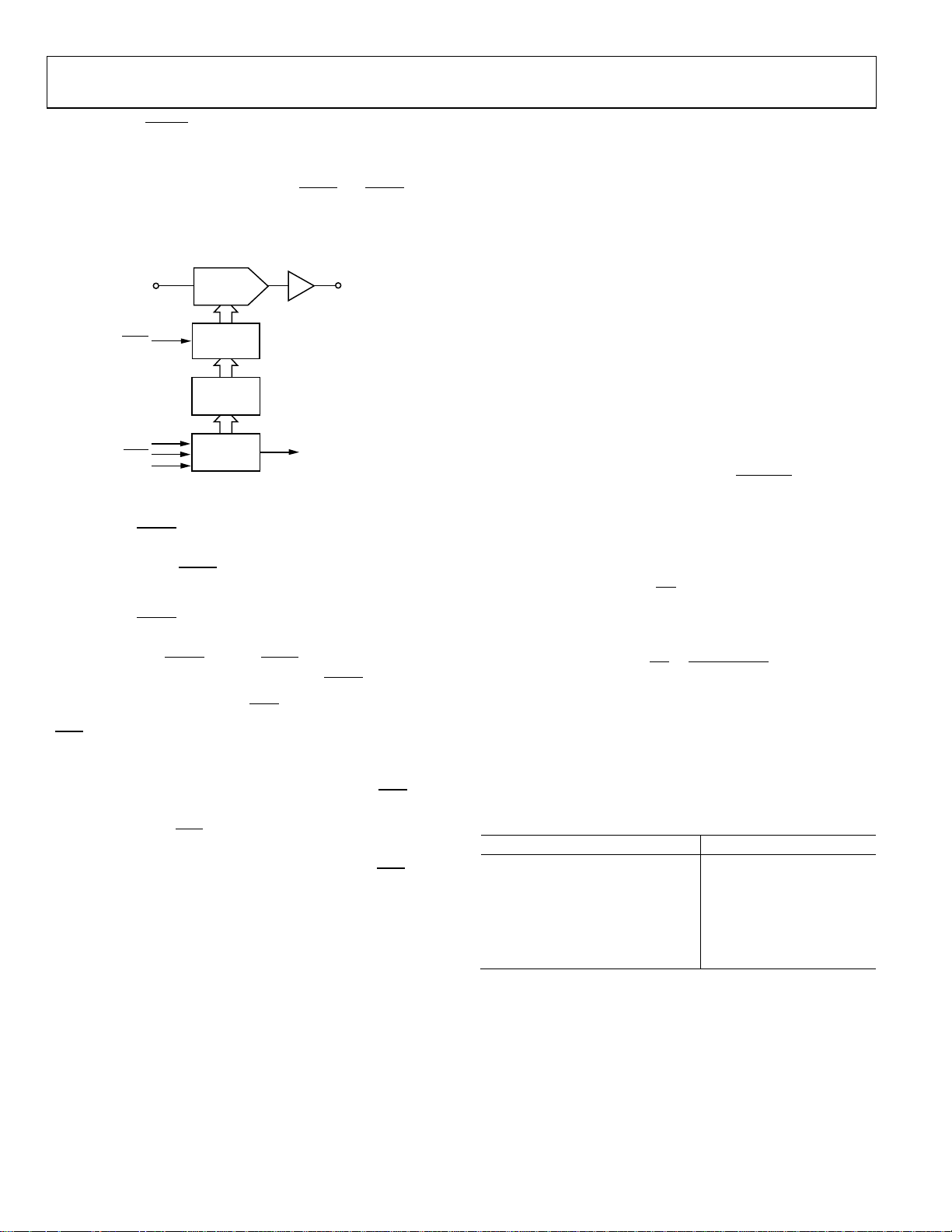
After data has been transferred into the input register of the
DACs, there are two ways to update the DAC registers and DAC
outputs. Depending on the status of both
SYNC
and
LDAC
, one
of two update modes is selected: individual DAC updating or
simultaneous updating of all DACs.
Figure 41. Simplified Diagram of Input Loading Circuitry for One DAC
Individual DAC Updating
In this mode,
LDAC
is held low while data is being clocked into
the input shift register. The addressed DAC output is updated
SYNC
on the rising edge of
.
Simultaneous Updating of All DACs
In this mode,
LDAC
is held high while data is being clocked
into the input shift register. All DAC outputs are asynchronously
LDAC
updated by taking
low after
The update now occurs on the falling edge of
ASYNCHRONOUS CLEAR (
CLR
is an active low clear that allows the outputs to clear to
SYNC
CLR
has been taken high.
LDAC
.
)
either zero-scale code or midscale code. The clear code value is
user-selectable via the CLR select bit of the control register (see
the Control Register section). It is necessary to maintain
CLR
low
for a minimum amount of time to complete the operation (see
Figure 2). When the
CLR
signal is returned high, the output
remains at the cleared value until a new value is programmed.
CLR
The outputs cannot update with a new value while the
pin
is low. A clear operation can also be performed via the clear
command in the control register.
CONFIGURING THE AD5724/AD5734/AD5754
When the power supplies are applied to the AD5724/AD5734/
AD5754, the power-on reset circuit ensures that all registers
default to 0. This places all channels in power-down mode.
The DV
are powered. If this is not done, the first write to the device may
be ignored. The first communication to the AD5724/AD5734/
AD5754 must be to set the required output range on all channels
(the default range is the 5 V unipolar range) by writing to the
output range select register. The user must then write to the
power control register to power on the required channels. To
program an output value on a channel, that channel must first
be powered up; any writes to a channel while it is in power-down
mode are ignored. The AD5724/AD5734/AD5754 operate with a
wide power supply range. It is important that the power supply
applied to the devices provides adequate headroom to support
the chosen output ranges.
TRANSFER FUNCTION
Tabl e 7 to Tab l e 15 show the relationships of the ideal input code
to output voltage for the AD5754, AD5734, and AD5724, respec-
tively, for all output voltage ranges. For unipolar output ranges,
the data coding is straight binary. For bipolar output ranges, the
data coding is user-selectable via the BIN/
be either offset binary or twos complement.
For a unipolar output range, the output voltage expression is
given by
For a bipolar output range, the output voltage expression is given by
where:
D is the decimal equivalent of the code loaded to the DAC.
N is the bit resolution of the DAC.
V
REFIN
Gain is an internal gain with a value that depends on the output
range selected by the user, as shown in Table 6.
Table 6. Internal Gain Values
Output Range (V) Gain Value
+5 2
+10 4
+10.8 4.32
±5 4
±10 8
must be brought high before any of the interface lines
CC
2sCOMP
pin and can
is the reference voltage applied at the REFIN pin.
Rev. F | Page 20 of 31
Page 21

Data Sheet AD5724/AD5734/AD5754
0000
0000
0000
0001
−2 × REFIN × (32,767/32,768)
−4 × REFIN × (32,767/32,768)
−4.32 × REFIN × (32,767/32,768)
0000
0000
0000
0000
−2 × REFIN × (32,768/32,768)
−4 × REFIN × (32,768/32,768)
−4.32 × REFIN × (32,768/32,768)
0000
0000
0000
0001
+2 × REFIN × (1/32,768)
+4 × REFIN × (1/32,768)
+4.32 × REFIN × (1/32,768)
Digital Input
Analog Output
1000
0000
0000
0000
+2 × REFIN × (32,768/65,536)
+4 × REFIN × (32,768/65,536)
+4.32 × REFIN × (32,768/65,536)
Ideal Output Voltage to Input Code Relationship—AD5754
Table 7. Bipolar Output, Offset Binary Coding
Digital Input Analog Output
MSB LSB ±5 V Output Range ±10 V Output Range ±10.8 V Output Range
1111 1111 1111 1111 +2 × REFIN × (32,767/32,768) +4 × REFIN × (32,767/32,768) +4.32 × REFIN × (32,767/32,768)
1111 1111 1111 1110 +2 × REFIN × (32,766/32,768) +4 × REFIN × (32,766/32,768) +4.32 × REFIN × (32,766/32,768)
… … … … … … …
1000 0000 0000 0001 +2 × REFIN × (1/32,768) +4 × REFIN × (1/32,768) +4.32 × REFIN × (1/32,768)
1000 0000 0000 0000 0 V 0 V 0 V
0111 1111 1111 1111 −2 × REFIN × (1/32,768) −4 × REFIN × (1/32,768) −4.32 × REFIN × (32,766/32,768)
… … … … … … …
Table 8. Bipolar Output, Twos Complement Coding
Digital Input Analog Output
MSB LSB ±5 V Output Range ±10 V Output Range ±10.8 V Output Range
0111 1111 1111 1111 +2 × REFIN × (32,767/32,768) +4 × REFIN × (32,767/32,768) +4.32 × REFIN × (32,767/32,768)
0111 1111 1111 1110 +2 × REFIN × (32,766/32,768) +4 × REFIN × (32,766/32,768) +4.32 × REFIN × (32,766/32,768)
… … … … … … …
0000 0000 0000 0000 0 V 0 V 0 V
1111 1111 1111 1111 −2 × REFIN × (1/32,768) −4 × REFIN × (1/32,768) −4.32 × REFIN × (1/32,768)
… … … … … … …
1000 0000 0000 0001 −2 × REFIN × (32,767/32,768) −4 × REFIN × (32,767/32,768) −4.32 × REFIN × (32,767/32,768)
1000 0000 0000 0000 −2 × REFIN × (32,768/32,768) −4 × REFIN × (32,768/32,768) −4.32 × REFIN × (32,768/32,768)
Table 9. Unipolar Output, Straight Binary Coding
MSB LSB +5 V Output Range +10 V Output Range +10.8 V Output Range
1111 1111 1111 1111 +2 × REFIN × (65,535/65,536) +4 × REFIN × (65,535/65,536) +4.32 × REFIN × (65,535/65,536)
1111 1111 1111 1110 +2 × REFIN × (65,534/65,536) +4 × REFIN × (65,534/65,536) +4.32 × REFIN × (65,534/65,536)
… … … … … … …
1000 0000 0000 0001 +2 × REFIN × (32,769/65,536) +4 × REFIN × (32,769/65,536) +4.32 × REFIN × (32,769/65,536)
0111 1111 1111 1111 +2 × REFIN × (32,767/65,536) +4 × REFIN × (32,767/65,536) +4.32 × REFIN × (32,767/65,536)
… … … … … … …
0000 0000 0000 0001 +2 × REFIN × (1/65,536) +4 × REFIN × (1/65,536) +4.32 × REFIN × (1/65,536)
0000 0000 0000 0000 0 V 0 V 0 V
Rev. F | Page 21 of 31
Page 22

AD5724/AD5734/AD5754 Data Sheet
00
0000
0000
0001
−2 × REFIN × (8191/8192)
−4 × REFIN × (8191/8192)
−4.32 × REFIN × (8191/8192)
00
0000
0000
0000
−2 × REFIN × (8192/8192)
−4 × REFIN × (8192/8192)
−4.32 × REFIN × (8192/8192)
00
0000
0000
0001
+2 × REFIN × (1/8192)
+4 × REFIN × (1/8192)
+4.32 × REFIN × (1/8192)
Digital Input
Analog Output
10
0000
0000
0000
+2 × REFIN × (8192/16,384)
+4 × REFIN × (8192/16,384)
+4.32 × REFIN × (8192/16,384)
Ideal Output Voltage to Input Code Relationship—AD5734
Table 10. Bipolar Output, Offset Binary Coding
Digital Input Analog Output
MSB LSB ±5 V Output Range ±10 V Output Range ±10.8 V Output Range
11 1111 1111 1111 +2 × REFIN × (8191/8192) +4 × REFIN × (8191/8192) +4.32 × REFIN × (8191/8192)
11 1111 1111 1110 +2 × REFIN × (8190/8192) +4 × REFIN × (8190/8192) +4.32 × REFIN × (8190/8192)
… … … … … … …
10 0000 0000 0001 +2 × REFIN × (1/8192) +4 × REFIN × (1/8192) +4.32 × REFIN × (1/8192)
10 0000 0000 0000 0 V 0 V 0 V
01 1111 1111 1111 −2 × REFIN × (1/8192) −4 × REFIN × (1/8192) −4.32 × REFIN × (1/8192)
… … … … … … …
Table 11. Bipolar Output, Twos Complement Coding
Digital Input Analog Output
MSB LSB ±5 V Output Range ±10 V Output Range ±10.8 V Output Range
01 1111 1111 1111 +2 × REFIN × (8191/8192) +4 × REFIN × (8191/8192) +4.32 × REFIN × (8191/8192)
01 1111 1111 1110 +2 × REFIN × (8190/8192) +4 × REFIN × (8190/8192) +4.32 × REFIN × (8190/8192)
… … … … … … …
00 0000 0000 0000 0 V 0 V 0 V
11 1111 1111 1111 −2 × REFIN × (1/8192) −4 × REFIN × (1/8192) −4.32 × REFIN × (1/8192)
… … … … … … …
10 0000 0000 0001 −2 × REFIN × (8191/8192) −4 × REFIN × (8191/8192) −4.32 × REFIN × (8191/8192)
10 0000 0000 0000 −2 × REFIN × (8192/8192) −4 × REFIN × (8192/8192) −4.32 × REFIN × (8192/8192)
Table 12. Unipolar Output, Straight Binary Coding
MSB LSB +5 V Output Range +10 V Output Range +10.8 V Output Range
11 1111 1111 1111 +2 × REFIN × (16,383/16,384) +4 × REFIN × (16,383/16,384) +4.32 × REFIN × (16,383/16,384)
11 1111 1111 1110 +2 × REFIN × (16,382/16,384) +4 × REFIN × (16,382/16,384) +4.32 × REFIN × (16,382/16,384)
… … … … … … …
10 0000 0000 0001 +2 × REFIN × (8193/16,384) +4 × REFIN × (8193/16,384) +4.32 × REFIN × (8193/16,384)
01 1111 1111 1111 +2 × REFIN × (8191/16,384) +4 × REFIN × (8191/16,384) +4.32 × REFIN × (8191/16,384)
… … … … … … …
00 0000 0000 0001 +2 × REFIN × (1/16,384) +4 × REFIN × (1/16,384) +4.32 × REFIN × (1/16,384)
00 0000 0000 0000 0 V 0 V 0 V
Rev. F | Page 22 of 31
Page 23

Data Sheet AD5724/AD5734/AD5754
0000
0000
0001
−2 × REFIN × (2047/2048)
−4 × REFIN × (2047/2048)
−4.32 × REFIN × (2047/2048)
0000
0000
0000
−2 × REFIN × (2048/2048)
−4 × REFIN × (2048/2048)
−4.32 × REFIN × (2048/2048)
0000
0000
0001
+2 × REFIN × (1/2048)
+4 × REFIN × (1/2048)
+4.32 × REFIN × (1/2048)
Digital Input
Analog Output
1000
0000
0000
+2 × REFIN × (2048/4096)
+4 × REFIN × (2048/4096)
+4.32 × REFIN × (2048/4096)
Ideal Output Voltage to Input Code Relationship—AD5724
Table 13. Bipolar Output, Offset Binary Coding
Digital Input Analog Output
MSB LSB ±5 V Output Range ±10 V Output Range ±10.8 V Output Range
1111 1111 1111 +2 × REFIN × (2047/2048) +4 × REFIN × (2047/2048) +4.32 × REFIN × (2047/2048)
1111 1111 1110 +2 × REFIN × (2046/2048) +4 × REFIN × (2046/2048) +4.32 × REFIN × (2046/2048)
… … … … … …
1000 0000 0001 +2 × REFIN × (1/2048) +4 × REFIN × (1/2048) +4.32 × REFIN × (1/2048)
1000 0000 0000 0 V 0 V 0 V
0111 1111 1111 −2 × REFIN × (1/2048) −4 × REFIN × (1/2048) −4.32 × REFIN × (1/2048)
… … … … … …
Table 14. Bipolar Output, Twos Complement Coding
Digital Input Analog Output
MSB LSB ±5 V Output Range ±10 V Output Range ±10.8 V Output Range
0111 1111 1111 +2 × REFIN × (2047/2048) +4 × REFIN × (2047/2048) +4.32 × REFIN × (2047/2048)
0111 1111 1110 +2 × REFIN × (2046/2048) +4 × REFIN × (2046/2048) +4.32 × REFIN × (2046/2048)
… … … … … …
0000 0000 0000 0 V 0 V 0 V
1111 1111 1111 −2 × REFIN × (1/2048) −4 × REFIN × (1/2048) −4.32 × REFIN × (1/2048)
… … … … … …
1000 0000 0001 −2 × REFIN × (2047/2048) −4 × REFIN × (2047/2048) −4.32 × REFIN × (2047/2048)
1000 0000 0000 −2 × REFIN × (2048/2048) −4 × REFIN × (2048/2048) −4.32 × REFIN × (2048/2048)
Table 15. Unipolar Output, Straight Binary Coding
MSB LSB +5 V Output Range +10 V Output Range +10.8 V Output Range
1111 1111 1111 +2 × REFIN × (4095/4096) +4 × REFIN × (4095/4096) +4.32 × REFIN × (4095/4096)
1111 1111 1110 +2 × REFIN × (4094/4096) +4 × REFIN × (4094/4096) +4.32 × REFIN × (4094/4096)
… … … … … …
1000 0000 0001 +2 × REFIN × (2049/4096) +4 × REFIN × (2049/4096) +4.32 × REFIN × (2049/4096)
0111 1111 1111 +2 × REFIN × (2047/4096) +4 × REFIN × (2047/4096) +4.32 × REFIN × (2047/4096)
… … … … … …
0000 0000 0001 +2 × REFIN × (1/4096) +4 × REFIN × (1/4096) +4.32 × REFIN × (1/4096)
0000 0000 0000 0 V 0 V 0 V
Rev. F | Page 23 of 31
Page 24
AD5724/AD5734/AD5754 Data Sheet
0 0 0 DAC A
R/W
Zero
REG2
REG1
REG0
A2
A1
A0
DB15 to DB2
DB1
DB0
INPUT SHIFT REGISTER
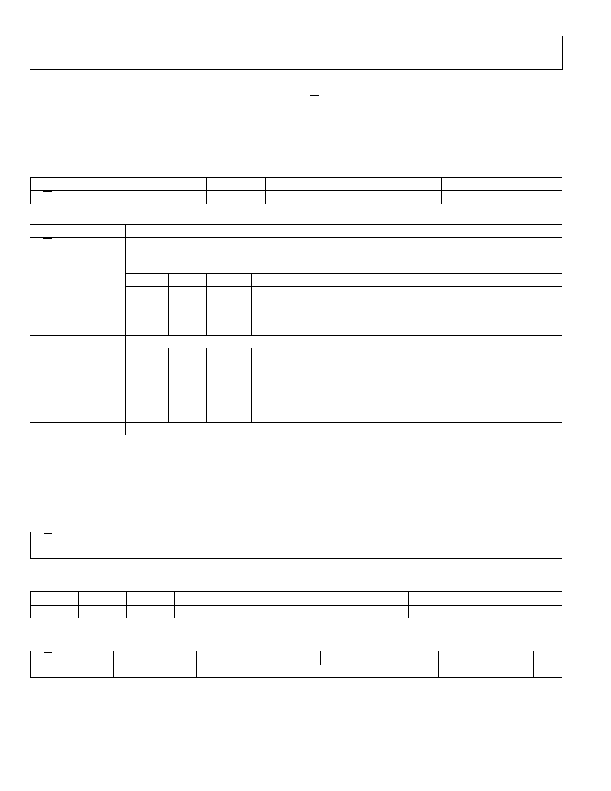
The input shift register is 24 bits wide and consists of a read/write bit (R/W), a reserved bit (zero) that must always be set to 0, three
register select bits (REG0, REG1, REG2), three DAC address bits (A2, A1, A0), and 16 data bits (data). The register data is clocked in MSB
first on the SDIN pin. Tabl e 16 shows the register format and Tab l e 17 describes the function of each bit in the register. All registers are
read/write registers.
Table 16. Input Register Format
MSB LSB
DB23 DB22 DB21 DB20 DB19 DB18 DB17 DB16 DB15 to DB0
R/W Zero REG2 REG1 REG0 A2 A1 A0 Data
Table 17. Input Register Bit Functions
Bit Mnemonic Description
R/W Indicates a read from or a write to the addressed register.
REG2, REG1, REG0 Used in association with the address bits to determine if a write operation is to the DAC register, the output range
select register, the power control register, or the control register.
0 0 0 DAC register
0 0 1 Output range select register
0 1 0 Power control register
0 1 1 Control register
A2, A1, A0 These DAC address bits are used to decode the DAC channels.
REG2 REG1 REG0 Function
A2 A1 A0 Channel Address
0 0 1 DAC B
0 1 0 DAC C
0 1 1 DAC D
1 0 0 All four DACs
DB15 to DB0 Data bits.
DAC REGISTER
The DAC register is addressed by setting the three REG bits to 000. The DAC address bits select the DAC channel where the data transfer
is to take place (see Tab l e 17). The data bits are in positions DB15 to DB0 for the AD5754 (see Table 18), DB15 to DB2 for the AD5734
(see Tabl e 19), and DB15 to DB4 for the AD5724 (see Tabl e 20).
Table 18. Programming the AD5754 DAC Register
MSB LSB
Zero REG2 REG1 REG0 A2 A1 A0 DB15 to DB0
R/
W
0 0 0 0 0 DAC address 16-bit DAC data
Table 19. Programming the AD5734 DAC Register
MSB LSB
0 0 0 0 0 DAC address 14-bit DAC data X X
Table 20. Programming the AD5724 DAC Register
MSB LSB
Zero REG2 REG1 REG0 A2 A1 A0 DB15 to DB4 DB3 DB2 DB1 DB0
R/
W
0 0 0 0 0 DAC address 12-bit DAC data X X X X
Rev. F | Page 24 of 31
Page 25
Data Sheet AD5724/AD5734/AD5754
0 0 1
+10
Option
Description
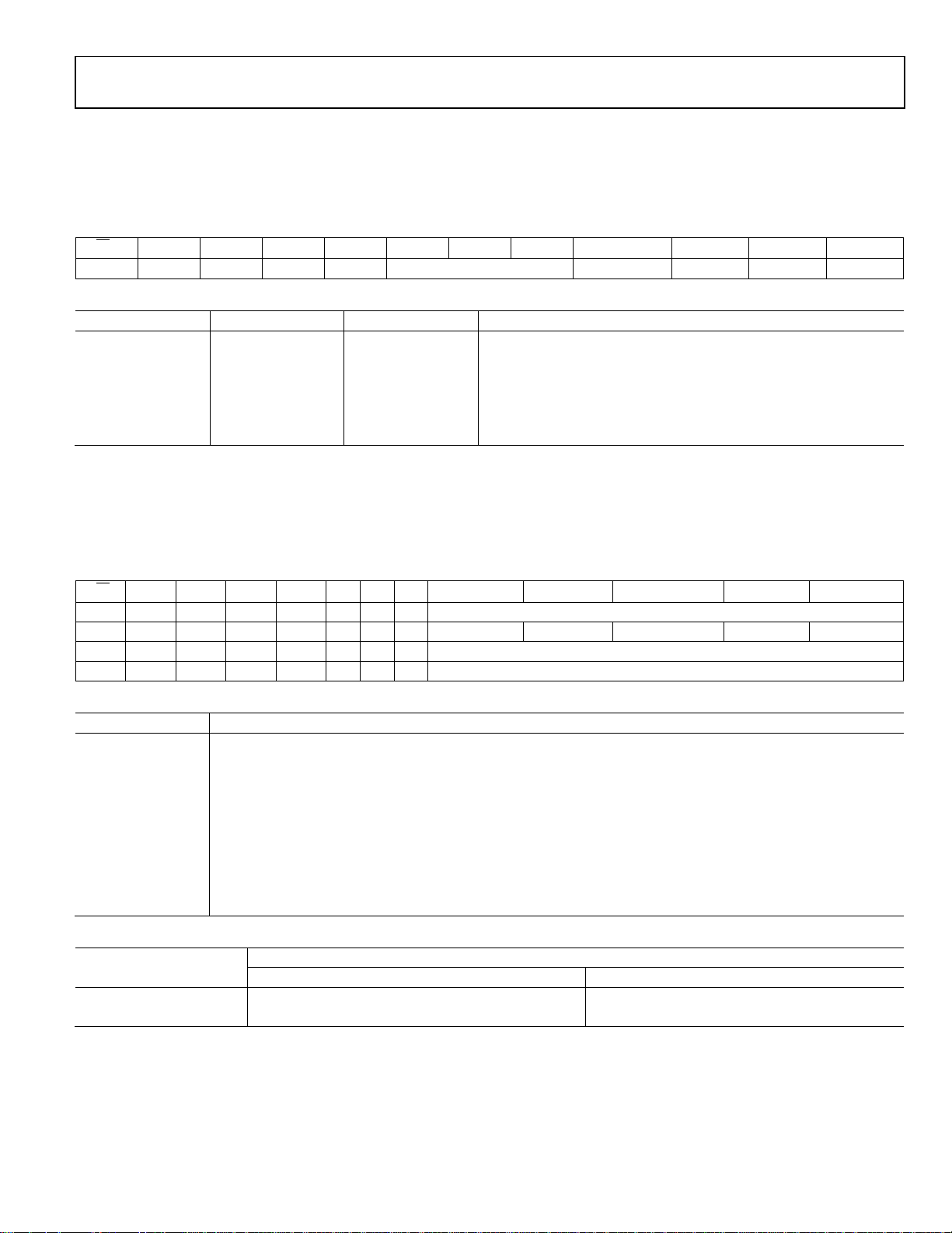
OUTPUT RANGE SELECT REGISTER
The output range select register is addressed by setting the three REG bits to 001. The DAC address bits select the DAC channel and the
range bits (R2, R1, R0) select the required output range (see Table 21 and Tab l e 22).
Table 21. Programming the Required Output Range
MSB LSB
Zero REG2 REG1 REG0 A2 A1 A0 DB15 to DB3 DB2 DB1 DB0
R/
W
0 0 0 0 1 DAC address Don’t care R2 R1 R0
Table 22. Output Range Options
R2 R1 R0 Output Range (V)
0 0 0 +5
0 1 0 +10.8
0 1 1 ±5
1 0 0 ±10
1 0 1 ±10.8
CONTROL REGISTER
The control register is addressed by setting the three REG bits to 011. The value written to the address and data bits determines the
control function selected. The control register options are shown in Tabl e 23 and Table 24.
Table 23. Programming the Control Register
MSB LSB
Zero REG2 REG1 REG0 A2 A1 A0 DB15 to DB4 DB3 DB2 DB1 DB0
R/
W
0 0 0 1 1 0 0 0 NOP, data = don’t care
0 0 0 1 1 0 0 1 Don’t care TSD enable Clamp enable CLR select SDO disable
0 0 0 1 1 1 0 0 Clear, data = don’t care
0 0 0 1 1 1 0 1 Load, data = don’t care
Table 24. Explanation of Control Register Options
NOP No operation instruction used in readback operations.
Clear Addressing this function sets the DAC registers to the clear code and updates the outputs.
Load Addressing this function updates the DAC registers and, consequently, the DAC outputs.
SDO Disable Set by the user to disable the SDO output. Cleared by the user to enable the SDO output (default).
CLR Select See Table 25 for a description of the CLR select operation.
Clamp Enable Set by the user to enable the current-limit clamp. The channel does not power down upon detection of an
overcurrent; the current is clamped at 20 mA (default).
Cleared by the user to disable the current-limit clamp. The channel powers down upon detection of an overcurrent.
TSD Enable Set by the user to enable the thermal shutdown feature. Cleared by the user to disable the thermal shutdown
feature (default).
Table 25. CLR Select Options
Output CLR Value
CLR Select Setting Unipolar Output Range Bipolar Output Range
0 0 V 0 V
1 Midscale Negative full scale
Rev. F | Page 25 of 31
Page 26
AD5724/AD5734/AD5754 Data Sheet
POWER CONTROL REGISTER
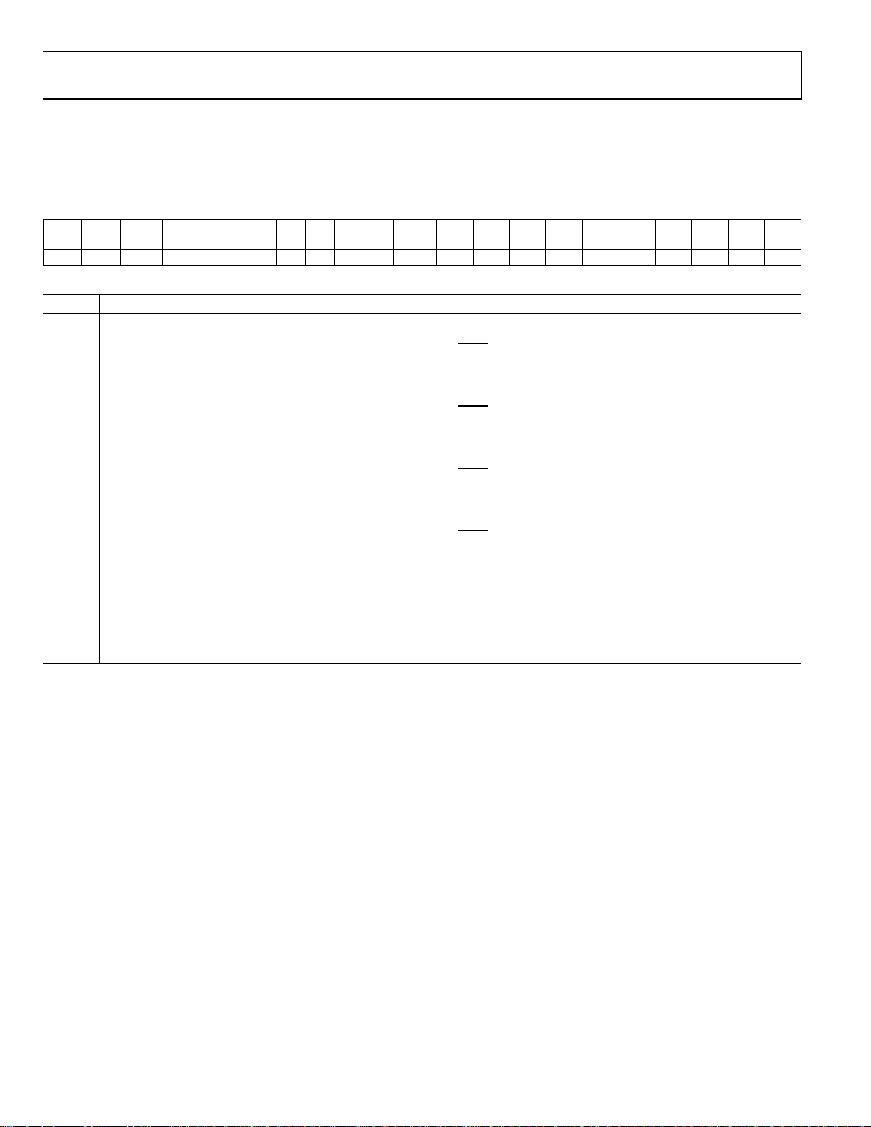
The power control register is addressed by setting the three REG bits to 010. This register allows the user to control and determine the
power and thermal status of the AD5724/AD5734/AD5754. The power control register options are shown in Tab l e 26 and Table 27.
Table 26. Programming the Power Control Register
MSB LSB
W
R/
Zero REG2 REG1 REG0 A2 A1 A0
0 0 0 1 0 0 0 0 X OCD OCC OCB OCA 0 TSD 0 PUD PUC PUB PUA
Table 27. Power Control Register Functions
Option Description
PUA DAC A power-up. When set, this bit places DAC A in normal operating mode. When cleared, this bit places DAC A in power-down
mode (default). After setting this bit to power DAC A, a power up time of 10 µs is required. During this power-up time, the DAC
register must not be loaded to the DAC output (see the Load DAC/
cleared, DAC A powers down automatically upon detection of an overcurrent, and PU
PUB DAC B power-up. When set, this bit places DAC B in normal operating mode. When cleared, this bit places DAC B in power-down
mode (default). After setting this bit to power DAC B, a power up time of 10 µs is required. During this power-up time, the DAC
register must not be loaded to the DAC output (see the Load DAC/
cleared, DAC B powers down automatically upon detection of an overcurrent, and PUB is cleared to reflect this.
PUC DAC C power-up. When set, this bit places DAC C in normal operating mode. When cleared, this bit places DAC C in power-down
mode (default). After setting this bit to power DAC C, a power up time of 10 µs is required. During this power-up time, the DAC
register must not be loaded to the DAC output (see the Load DAC/
cleared, DAC C powers down automatically upon detection of an overcurrent, and PUC is cleared to reflect this.
PUD DAC D power-up. When set, this bit places DAC D in normal operating mode. When cleared, this bit places DAC D in power-down
mode (default). After setting this bit to power DAC D, a power up time of 10 µs is required. During this power-up time, the DAC
register must not be loaded to the DAC output (see the Load DAC/
cleared, DAC D powers down automatically upon detection of an overcurrent, and PU
TSD Thermal shutdown alert. Read-only bit. In the event of an overtemperature situation, the four DACs are powered down and this
bit is set.
OCA DAC A overcurrent alert. Read-only bit. In the event of an overcurrent situation on DAC A, this bit is set.
OCB DAC B overcurrent alert. Read-only bit. In the event of an overcurrent situation on DAC B, this bit is set.
OCC DAC C overcurrent alert. Read-only bit. In the event of an overcurrent situation on DAC C, this bit is set.
OCD DAC D overcurrent alert. Read-only bit. In the event of an overcurrent situation on DAC D, this bit is set.
DB15 to
DB11
DB10 DB9 DB8 DB7 DB6 DB5 DB4 DB3 DB2 DB1 DB0
section). If the clamp enable bit of the control register is
LDAC
is cleared to reflect this.
A
section). If the clamp enable bit of the control register is
LDAC
section). If the clamp enable bit of the control register is
LDAC
section). If the clamp enable bit of the control register is
LDAC
is cleared to reflect this.
D
Rev. F | Page 26 of 31
Page 27
Data Sheet AD5724/AD5734/AD5754
FEATURES
ANALOG OUTPUT CONTROL
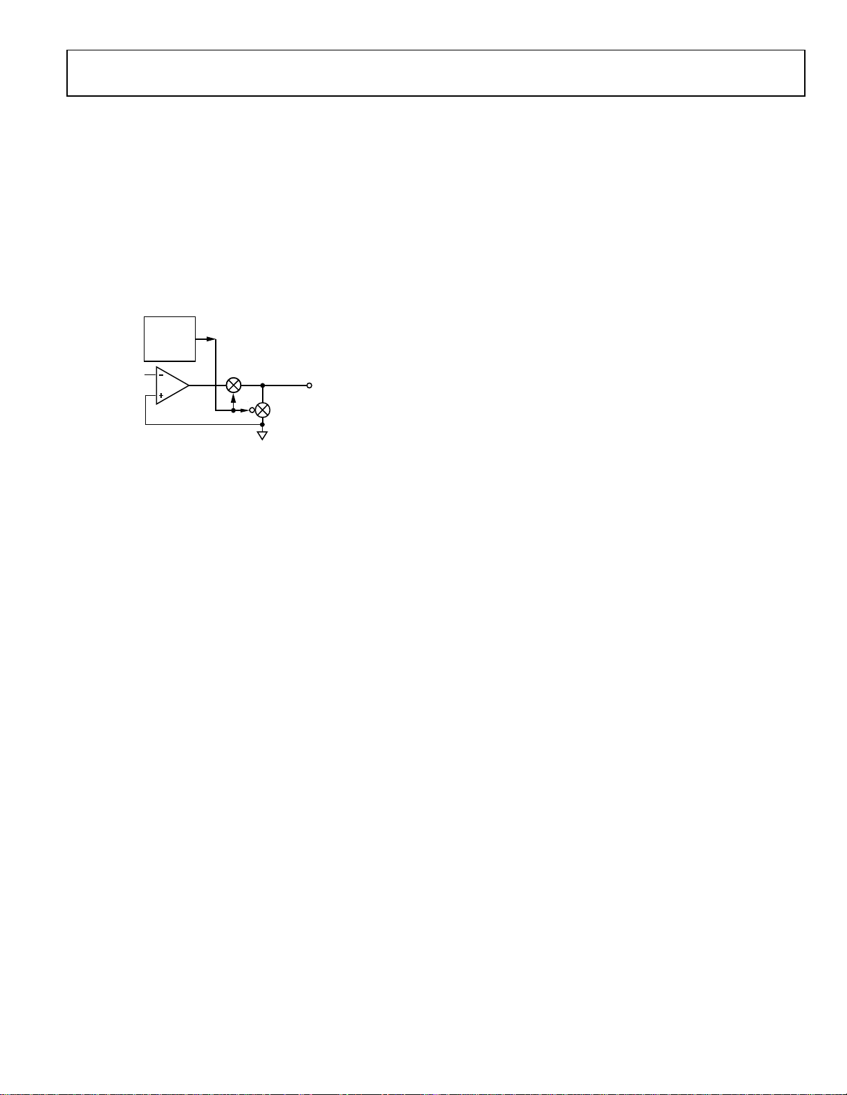
In many industrial process control applications, it is vital to control
the output voltage during power-up. When the supply voltages
change during power-up, the V
x pins are clamped to 0 V via
OUT
a low impedance path (approximately 4 kΩ). To prevent the output
amplifiers from being shorted to 0 V during this time, Transmission Gate G1 is also opened (see Figure 42). These conditions
are maintained until the analog power supplies have stabilized
and a valid word is written to a DAC register. At this time, G2
opens and G1 closes.
VOLTAGE
MONITOR
AND
CONTROL
G1
V
A
G2
Figure 42. Analog Output Control Circuitry
OUT
6468-010
POWER-DOWN MODE
Each DAC channel of the AD5724/AD5734/AD5754 can be
individually powered down. By default, all channels are in powerdown mode. The power status is controlled by the power control
register (see Table 26 and Table 27 for details). When a channel
is in power-down mode, the output pin is clamped to ground
through a resistance of approximately 4 kΩ and the output of
the amplifier is disconnected from the output pin.
OVERCURRENT PROTECTION
Each DAC channel of the AD5724/AD5734/AD5754 incorporates
individual overcurrent protection. The user has two options for
the configuration of the overcurrent protection: constant current
clamp or automatic channel power-down. The configuration of
the overcurrent protection is selected via the clamp enable bit in
the control register.
Constant Current Clamp (Clamp Enable = 1)
If a short circuit occurs in this configuration, the current is
clamped at 20 mA. This event is signaled to the user by the
setting of the appropriate overcurrent (OC
) bit in the power
X
control register. Upon removal of the short-circuit fault, the
bit is cleared.
OC
X
Automatic Channel Power-Down (Clamp Enable = 0)
If a short circuit occurs in this configuration, the shorted
channel powers down and the output is clamped to ground via a
resistance of approximately 4 kΩ. At this time, the output of the
amplifier is disconnected from the output pin. The short-circuit
event is signaled to the user via the overcurrent (OC
the power-up (PU
) bits indicate which DACs have powered
X
) bits, and
X
down. After the fault is rectified, the channels can be powered
up again by setting the PU
bits.
X
THERMAL SHUTDOWN
The AD5724/AD5734/AD5754 incorporate a thermal shutdown
feature that automatically shuts down the device if the core temperature exceeds approximately 150°C. The thermal shutdown
feature is disabled by default and can be enabled via the TSD enable
bit of the control register. In the event of a thermal shutdown,
the TSD bit of the power control register is set.
Rev. F | Page 27 of 31
Page 28
AD5724/AD5734/AD5754 Data Sheet
V
APPLICATIONS INFORMATION
+5 V/±5 V OPERATION
When operating from a single +5 V supply or a dual ±5 V
supply, an output range of +5 V or ±5 V is not achievable because
sufficient headroom for the output amplifier is not available. In
this situation, a reduced reference voltage can be used. For example,
a 2 V reference voltage produces an output range of +4 V or ±4 V,
and the 1 V of headroom is more than enough for full operation. A
standard value voltage reference of 2.048 V can be used to produce
output ranges of +4.096 V and ±4.096 V.
ALTERNATIVE POWER-UP SEQUENCE SUPPORT
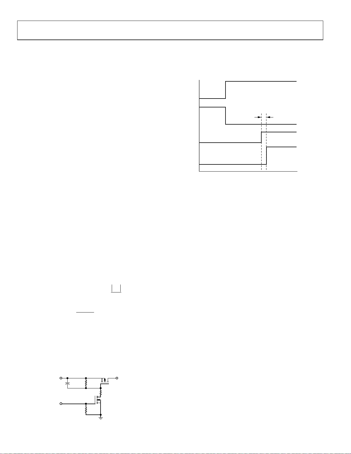
There may be cases where it is not possible to use the
recommended power-up sequence, and in those instances an
external circuit shown in Figure 43 is recommended to be used.
The circuit shown in Figure 43 ensures that the digital block is
powered up first, prior to the analog block, by using a load
switch circuit. This circuit targets applications for which either
AV
or AVSS or both supplies power up before DVCC.
DD
Consider the following design rules when choosing the
component values for the AV
R1 ensures that the Q1 gate to source voltage is zero when
is in an open state. R1 also prevents false turn on of
DV
CC
Q1. However, if DV
source, R1 can be removed to conserve power.
Select Q1 (N-channel MOSFET) with a V
is much lower than the minimum operating DV
V
rating much lower than the maximum operating AVDD.
DS
C1, R2, and R3 are the main components that dictates the
delay from DV
enable to AVDD. Adjust the values
CC
according for the desired delay. Choose R2 and R3 values
that ensure Q2 turn on.
DELAY
where
Q2 (P-channel MOSFET) acts as a switch that allows the flow
of current from V
with very low R
AVV
EQ
DD
IN
DSON
operation. Other parameters such as maximum V
maximum drain to source current rating, V
voltage, and maximum gate to source voltage rating must
also be taken into consideration when choosing Q2.
IN
+
C1
LOAD SWITCH
SECTION
DV
CC
CONTROL
SECTION
Figure 43. Load Switch Control Circuit
delay circuit.
DD
is permanently connected to the
CC
threshold that
GS
and a
CC
RRCt 1ln)||()sec(
231
R
3
RR
23
V
GS
V
EQ
to AVDD; therefore, choosing a MOSFET
is necessary to minimize losses during
rating,
DS
threshold
GS
AV
Q2
R3
R2
Q1
R1
DD
06468-143
Rev. F | Page 28 of 31
Figure 44 shows an example of the analog supplies powering up
before the digital supply. The circuit delays the AV
until after DV
, as shown by the AVDD (delayed) line.
CC
AV
DD
AV
SS
DV
CC
AVDD(DELAYED)
Figure 44. Delayed Power Supplies Sequence Example
t (sec)
power up
DD
6468-144
LAYOUT GUIDELINES
In any circuit where accuracy is important, careful consideration of
the power supply and ground return layout helps to ensure the
rated performance. The printed circuit board on which the
AD5724/AD5734/AD5754 are mounted must be designed so the
analog and digital sections are separated and confined to certain
areas of the board. If the AD5724/AD5734/AD5754 are in a system
where multiple devices require an AGND to DGND connection,
the connection must be made at one point only. The star ground
point must be established as close as possible to the device.
The AD5724/AD5734/AD5754 must have ample supply bypassing
of a 10 μF capacitor in parallel with a 0.1 μF capacitor on each
supply located as close to the package as possible, ideally right up
against the device. The 10 μF capacitor is the tantalum bead type.
The 0.1 μF capacitor must have low effective series resistance (ESR)
and low effective series inductance (ESI), such as the common
ceramic types, which provide a low impedance path to ground
at high frequencies to handle transient currents due to internal
logic switching.
The power supply lines of the AD5724/AD5734/AD5754 must
use as large a trace as possible to provide low impedance paths
and reduce the effects of glitches on the power supply line. Fast
switching signals, such as a data clock, must be shielded with
digital ground to avoid radiating noise to other devices of the
board, and must never run near the reference inputs. A ground
line routed between the SDIN and SCLK lines helps reduce
crosstalk between them (this is not required on a multilayer
board that has a separate ground plane, but separating the lines
does help). It is essential to minimize noise on the REFIN line
because any unwanted signals couple through to the DAC
outputs.
Avoid crossover of digital and analog signals. Traces on opposite
sides of the board must run at right angles to each other. This
reduces the effects of feedthrough on the board. A microstrip
Page 29
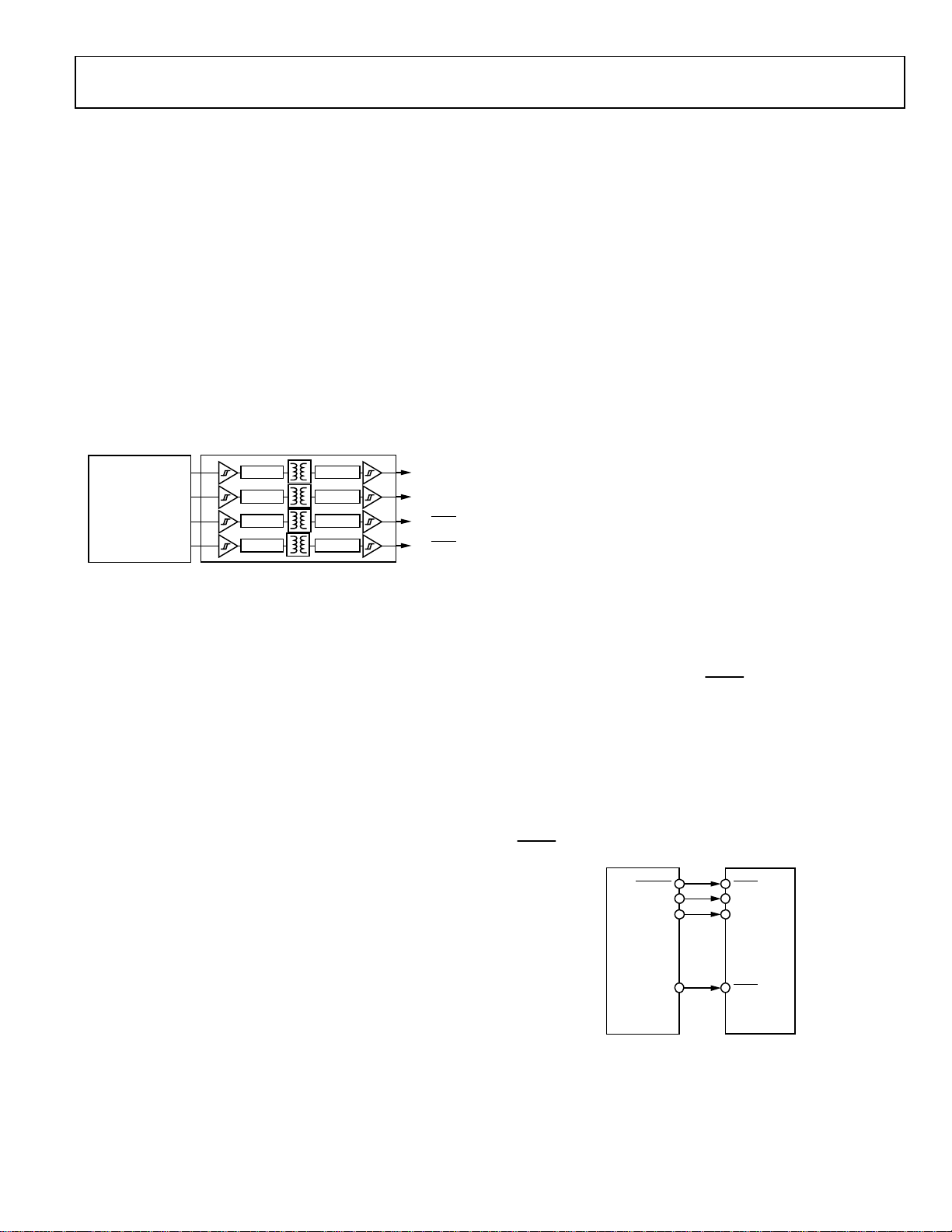
Data Sheet AD5724/AD5734/AD5754
A
technique is by far the best method, but it is not always possible
with a double-sided board. In this technique, the component
side of the board is dedicated to a ground plane and signal
traces are placed on the solder side.
GALVANICALLY ISOLATED INTERFACE
In many process control applications, it is necessary to provide
an isolation barrier between the controller and the unit being
controlled to protect and isolate the controlling circuitry from
any hazardous common-mode voltages that may occur. The
iCoupler® family of products from Analog Devices, Inc., provides
voltage isolation in excess of 2.5 kV. The serial loading structure
of the AD5724/AD5734/AD5754 makes them ideal for isolated
interfaces because the number of interface lines is kept to a
minimum. Figure 45 shows a 4-channel isolated interface to the
AD5724/AD5734/AD5754 using an ADuM1400. For further
information, visit http://www.analog.com/icouplers.
MICROCONTROLLER
V
SERIAL CLOCK OUT
SERIAL DATA OUT
SYNC OUT
CONTROL OUT
*ADDITIONAL PINS OMITTED FOR CLARITY.
IA
V
IB
V
IC
V
ID
Figure 45. Isolated Interface
DuM1400*
ENCODE DECODE
ENCODE DECODE
ENCODE DECODE
ENCODE DECODE
V
OA
TO SCLK
V
OB
TO SDIN
V
OC
TO SYNC
V
OD
TO LDAC
VOLTAGE REFERENCE SELECTION
To achieve optimum performance from the AD5724/AD5734/
AD5754 over the full operating temperature range of the devices, a
precision voltage reference must be used. Thought must be given to
the selection of a precision voltage reference. The voltage applied to
the reference inputs are used to provide a buffered positive and
negative reference for the DAC cores. Therefore, any error in
the voltage reference is reflected in the outputs of the device.
There are four possible sources of error to consider when
choosing a voltage reference for high accuracy applications:
initial accuracy, temperature coefficient of the output voltage,
long-term drift, and output voltage noise.
Initial accuracy error on the output voltage of an external
reference can lead to a full-scale error in the DAC. Therefore,
to minimize these errors, a reference with low initial accuracy
error specification is preferred. Choosing a reference with
an output trim adjustment, such as the ADR421, allows a
system designer to trim out system errors by setting the
reference voltage to a voltage other than the nominal. The trim
adjustment can also trim out temperature-induced errors.
06468-011
The temperature coefficient of a reference output voltage
affects INL, DNL, and TUE. A reference with a tight
temperature coefficient specification must be chosen to
reduce the dependence of the DAC output voltage on
ambient conditions.
Long-term drift is a measure of how much the reference
output voltage drifts over time. A reference with a tight
long-term drift specification ensures that the overall
solution remains relatively stable over the entire lifetime.
Consider reference output voltage noise in high accuracy
applications that have relatively low noise budgets. It is
important to choose a reference with as low an output
noise voltage as practical for the required system resolution.
Precision voltage references such as the ADR431 (XFET®
design) produce low output noise in the 0.1 Hz to 10 Hz
range. However, as the circuit bandwidth increases,
filtering the output of the reference may be required to
minimize the output noise.
MICROPROCESSOR INTERFACING
Microprocessor interfacing to the AD5724/AD5734/AD5754 is
via a serial bus that uses standard protocol compatible with microcontrollers and DSP processors. The communications channel
is a 3-wire (minimum) interface consisting of a clock signal, a
data signal, and a synchronization signal. The AD5724/AD5734/
AD5754 require a 24-bit data-word with data valid on the
falling edge of SCLK.
For all interfaces, the DAC output update can be initiated
automatically when all the data is clocked in, or it can be
LDAC
performed under the control of
registers can be read using the readback function.
AD5724/AD5734/AD5754 to Blackfin® DSP Interface
Figure 46 shows how the AD5724/AD5734/AD5754 can be interfaced to the Analog Devices Blackfin DSP. The Blackfin has an
integrated SPI port that can be connected directly to the SPI pins of
the AD5724/AD5734/AD5754 and the programmable I/O pins
that can be used to set the state of a digital input such as the
LDAC
pin.
SPISELx
SCK
MOSI
ADSP-BF531
PF10
. The contents of the
SYNC
SCLK
SDIN
AD5724/
AD5734/
AD5754
LDAC
06468-012
Figure 46. AD5724/AD5734/AD5754 to Blackfin Interface
Rev. F | Page 29 of 31
Page 30

AD5724/AD5734/AD5754 Data Sheet
Table 28. Some Precision References Recommended for Use with the AD5724/AD5734/AD5754
Part No. Initial Accuracy (mV Max) Long-Term Drift (ppm Typ) Temp Drift (ppm/°C Max) 0.1 Hz to 10 Hz Noise (µV p-p Typ)
ADR431 ±1 40 3 3.5
ADR421 ±1 50 3 1.75
ADR03 ±2.5 50 3 6
ADR291 ±2 50 8 8
AD780 ±1 20 3 4
Rev. F | Page 30 of 31
Page 31
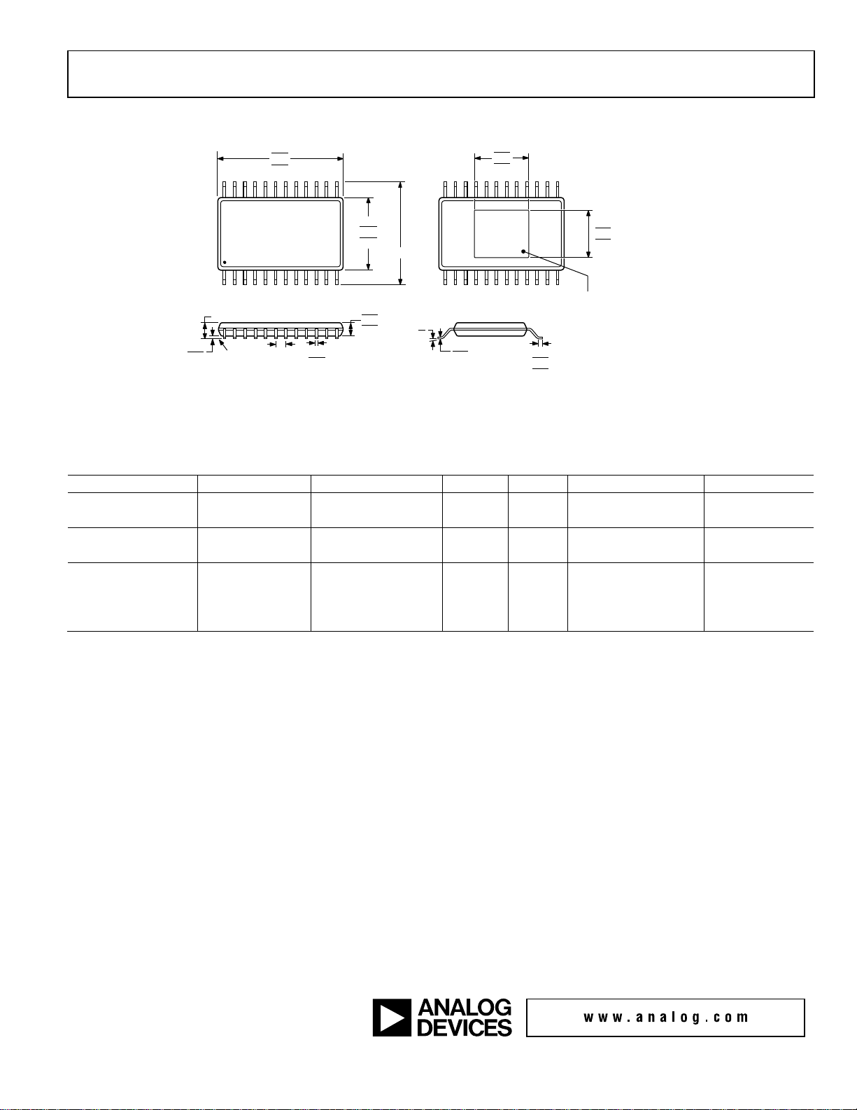
Data Sheet AD5724/AD5734/AD5754
COMPLIANT
TO JEDEC ST
ANDARDS MO-153-ADT
061708-A
24
13
121
6.40 BSC
0.15
0.05
0.10 COPLANARI T
Y
T
OP
VIEW
EXPOSED
P
AD
(Pins Up)
BOT
T
OM VIEW
4.50
4.40
4.30
7.90
7.80
7.70
1.20 MAX
1.05
1.00
0.80
0.65
BSC
0.30
0.19
SEATING
PLANE
0.20
0.09
8°
0°
0.75
0.60
0.45
5.02
5.00
4.95
3.25
3.20
3.15
FOR PROPE R CONNECTIO N OF
THE EXPOSED PAD, REFER TO
THE PIN CONFIGURATION AND
FUNCTIO N DES CRIPTIO NS
SECTION OF THIS DATA SHEET.
AD5754AREZ
16
−40°C to +85°C
0.3% FSR
±16 LSB
24-Lead TSSOP_EP
RE-24
©2008–2017 Analog Devices, Inc. All rights reserved. Trademarks and
OUTLINE DIMENSIONS
Figure 47. 24-Lead Thin Shrink Small Outline Package, Exposed Pad [TSSOP_EP]
(RE-24)
Dimensions shown in millimeters
ORDERING GUIDE
Model1 Resolution (Bits) Temperature Range TUE INL Package Description Package Option
AD5724AREZ 12 −40°C to +85°C 0.3% FSR ±1 LSB 24-Lead TSSOP_EP RE-24
AD5724AREZ-REEL7 12 −40°C to +85°C 0.3% FSR ±1 LSB 24-Lead TSSOP_EP RE-24
AD5734AREZ 14 −40°C to +85°C 0.3% FSR ±4 LSB 24-Lead TSSOP_EP RE-24
AD5734AREZ-REEL7 14 −40°C to +85°C 0.3% FSR ±4 LSB 24-Lead TSSOP_EP RE-24
AD5754AREZ-REEL7 16 −40°C to +85°C 0.3% FSR ±16 LSB 24-Lead TSSOP_EP RE-24
AD5754BREZ 16 −40°C to +85°C 0.1% FSR ±16 LSB 24-Lead TSSOP_EP RE-24
AD5754BREZ-REEL7 16 −40°C to +85°C 0.1% FSR ±16 LSB 24-Lead TSSOP_EP RE-24
1
Z = RoHS Compliant Part.
registered trademarks are the property of their respective owners.
D06468-0-2/17(F)
Rev. F | Page 31 of 31
 Loading...