

Page 1
AMD Socket 940
Qualification Plan
Publication #
Issue Date:
30353
September 2003
Revision:
3.04
Page 2

© 2003 Advanced Micro Devices, Inc. All rights reserved.
The contents of this document are provided in connection with Advanced
Micro Devices, Inc. (“AMD”) products. AMD makes no representations or
warranties with respect to the accuracy or completeness of the contents of this
publication and reserves the right to make changes to specifications and
product descriptions at any time without notice. No license, whether express,
implied, arising by estoppel, or otherwise, to any intellectual property rights are
granted by this publication. Except as set forth in AMD’s Standard Terms and
Conditions of Sale, AMD assumes no liability whatsoever, and disclaims any
express or implied warranty, relating to its products including, but not limited
to, the implied warranty of merchantability, fitness for a particular purpose, or
infringement of any intellectual property right.
AMD’s products are not designed, intended, authorized or warranted for use as
components in systems intended for surgical implant into the body, or in other
applications intended to support or sustain life, or in any other application in
which the failure of AMD’s product could create a situation where personal
injury, death, or severe property or environmental damage may occur. AMD
reserves the right to discontinue or make changes to its products at any time
without notice.
Trademarks
AMD, the AMD Arrow logo, AMD Athlon, AMD Opteron, and combinations thereof, are trademarks of
Advanced Micro Devices, Inc.
Other product names used in this publication are for identification purposes only and may be trademarks of their
respective companies.
Page 3

30353 Rev. 3.04 September 2003
AMD Socket 940 Qualification Plan
Contents
Revision History...............................................................................................................................7
Chapter 1 Introduction.............................................................................................................. 9
1.1 Purpose...............................................................................................................................9
1.2 Scope..................................................................................................................................9
1.3 Supplier Qualification Testing...........................................................................................9
Chapter 2 Socket 940 QualificationTests...............................................................................11
2.1 Qualification Test Report.................................................................................................11
2.2 Testing .............................................................................................................................12
2.3 Reference Documents ......................................................................................................13
Chapter 3 Documentation Requirements ..............................................................................15
Chapter 4 Mechanical and Environmental Test Procedures, Conditions, and
Requirements..........................................................................................................17
Chapter 5 Electrical Qualification Requirements.................................................................23
5.1 Fixture for Electrical Qualification Testing.....................................................................23
5.2 Electrical Specifications ..................................................................................................23
5.3 Inductance Measurements................................................................................................26
5.3.1 Capacitance and Inductance Matrices......................................................................26
5.3.2 Mated Partial Self-Inductance..................................................................................27
5.3.3 Mated Loop Inductance ...........................................................................................27
5.3.4 Mated Partial Loop Inductance Matrix....................................................................27
5.4 Capacitance Measurements..............................................................................................29
5.4.1 Test Procedures........................................................................................................29
5.4.2 Test Condition..........................................................................................................29
5.4.3 Requirements ...........................................................................................................29
5.5 Differential Impedance ....................................................................................................29
5.5.1 Differential Impedance Measurement......................................................................30
5.6 Propagation Delay Measurements ...................................................................................31
5.6.1 Single-Ended Propagation Delay Skew...................................................................31
Contents 3
Page 4
AMD Socket 940 Qualification Plan
30353 Rev. 3.04 September 2003
5.6.2 Differential Propagation Delay Skew ..................................................................... 32
5.7 Single-Ended and Differential Crosstalk......................................................................... 33
5.7.1 Test Procedure......................................................................................................... 33
5.7.2 Test Condition ......................................................................................................... 33
5.7.3 Requirements........................................................................................................... 33
4 Contents
Page 5

30353 Rev. 3.04 September 2003
AMD Socket 940 Qualification Plan
List of Figures
Figure 1. Socket 940 Qualification Test Matrix ..............................................................................12
Figure 2. Pin Configurations for the Maxwell Capacitance and Partial Inductance Matrix
Measurement ....................................................................................................................26
Figure 3. Loop Measurements for Extracting [Lp] for a Mated Three-Pin Combination. ..............28
Figure 4. Current/Voltage Definitions and Equivalent Circuit of the Partial Loop Inductance
Matrix ...............................................................................................................................28
Figure 5. Pin Configurations for the Propagation Delay Skew Measurements of Single-Ended
Signals. .............................................................................................................................31
List of Figures 5
Page 6

AMD Socket 940 Qualification Plan
30353 Rev. 3.04 September 2003
List of Tables
Table 1. Mechanical Qualification Test Descriptions..................................................................... 17
Table 2. Summary of Required Electrical Measurements for Socket 940 ...................................... 23
6 List of Tables
Page 7
30353 Rev. 3.04 September 2003
AMD Socket 940 Qualification Plan
Revision History
Date Revision Changes
September 2003
September 2003
June 2003
June 2003
June 2003
3.04
3.03
3.02
3.01
3.00
Third public release.
Internal Revision.
Second public release.
Internal Revision.
Initial Public Release
Revision History 7
Page 8
AMD Socket 940 Qualification Plan
30353 Rev. 3.04 September 2003
8 Revision History
Page 9

30353 Rev. 3.04 September 2003
AMD Socket 940 Qualification Plan
Chapter 1 Introduction
This document defines the qualification testing requirements for The AMD Socket 940. The
AMD Socket 940 is a 940-position, 1.27mm pitch, surface mount technology (SMT), zero
insertion force (ZIF) socket for use with Advanced Micro Devices (AMD) 940-pin ceramic micropin-grid-array (µPGA) package.
1.1 Purpose
This document describes the qualification testing procedures, conditions, and measurements
necessary to satisfy dimensional, mechanical, electrical, and reliability requirements for the Socket
940 that are necessary to meet the performance requirements of AMD Athlon™ 64 FX processor
or AMD Opteron™ processor products.
1.2 Scope
The qualification tests described in this document are used for qualifying the 940-position µPGA
ZIF socket designed to mate with the 940-pin µPGA package for the AMD Athlon 64 FX
processor or AMD Opteron processor. A supplier’s socket product must pass all requirements
listed in this document before it can be considered for approval.
1.3 Supplier Qualification Testing
To become an AMD Qualified Supplier for Socket 940, the potential socket supplier must
demonstrate that their product meets the requirements listed in this document and the AMD Socket
940 Design Specification, order# 25766.
The supplier is responsible for qualification testing costs.
Chapter 1 Introduction 9
Page 10
AMD Socket 940 Qualification Plan
30353 Rev. 3.04 September 2003
10 Introduction Chapter 1
Page 11

30353 Rev. 3.04 September 2003
AMD Socket 940 Qualification Plan
Chapter 2 Socket 940 QualificationTests
All qualification testing must be conducted in AMD-designated test facilities. Qualification
testing must be performed on production lots of Socket 940.
2.1 Qualification Test Details
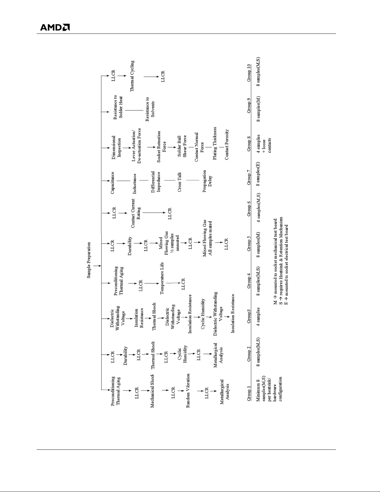
The socket qualification test matrix for Socket 940 is shown in Figure 1 on page 12, for the 10 test
groups. Each test group shows the sequence that the different tests must be performed. Test
procedures, conditions, and requirements for the 9 of the 10 test groups are listed in Chapter 4,
Mechanical and Environmental Test Procedures, Conditions, and Requirements, on page 17. Test
group 7, is covered in Chapter 5, Electrical Qualification Requirements, on page 23.
2.2 Qualification Test Report
A Qualification Test Report must be issued listing the results from all the test groups shown in
Figure 1 on page 12. This report must contain the following information for each of the tests
conducted:
• Title of the test
• Sample description
• Supplier lot numbers
• Test equipment used
• Test procedures
• Test date and name of tester
• Measurements and observations
• Results including raw data and/or sample calculations
Chapter 2 Socket 940 QualificationTests 11
Page 12
AMD Socket 940 Qualification Plan
30353 Rev. 3.04 September 2003
Figure 1. Socket 940 Qualification Test Matrix
12 Socket 940 QualificationTests Chapter 2
Page 13

30353 Rev. 3.04 September 2003
AMD Socket 940 Qualification Plan
2.3 Testing
Please contact the local AMD field application engineer (FAE) for approved test laboratory
locations. The local AMD FAE can be reached at 1-800-538-8450.
2.4 Reference Documents
AMD Socket 940 Design Specification, order# 25766 and EIA Standard, EIA 364, Electrical
Connector/Socket Test Procedures Including Environmental Classifications, contain additional
information for the qualification testing of the AMD Socket 940.
Socket 940 QualificationTests 13
Page 14
AMD Socket 940 Qualification Plan
30353 Rev. 3.04 September 2003
14 Socket 940 QualificationTests Chapter 2
Page 15

30353 Rev. 3.04 September 2003
AMD Socket 940 Qualification Plan
Chapter 3 Documentation Requirements
The supplier of the Socket 940 must submit a minimum amount of documentation to AMD
including:
• Socket 940 drawings and recommended PCB layout guidelines
• Socket 940 specifications
• Supplier part number for the specific Socket 940
• Electrical performance modeling
• Qualification Test Report—passing all the tests in this qualification plan
• Meeting all requirements of AMD Socket 940 Design Specification
• First article inspection report
In addition to the documentation, socket suppliers must provide AMD with five socket samples
from the qualification test lot.
The documentation package, as specified in Chapter 2 on page 11, must be submitted to AMD. If
all testing parameters are met, AMD will add the Socket 940 supplier data to the AMD
development partners listing.
Chapter 3 Documentation Requirements 15
Page 16
AMD Socket 940 Qualification Plan
30353 Rev. 3.04 September 2003
16 Documentation Requirements Chapter 3
Page 17
30353 Rev. 3.04 September 2003
AMD Socket 940 Qualification Plan
Chapter 4 Mechanical and Environmental
Test Procedures, Conditions, and
Requirements
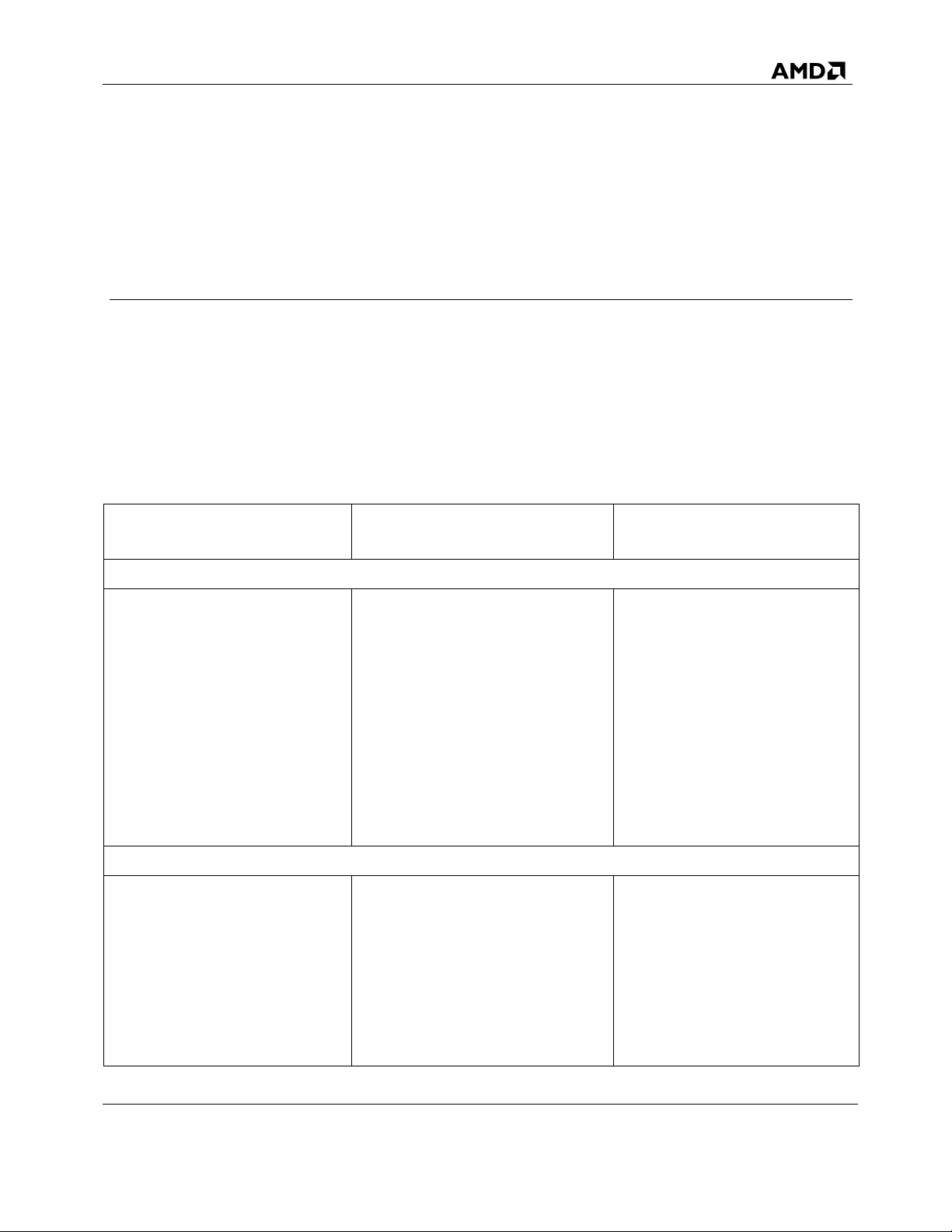
All test groups shown in Figure 1 on page 12 are covered in this chapter with the exception of test
group 7. Test group 7, is covered in Chapter 5, Electrical Qualification Requirements, on page 23.
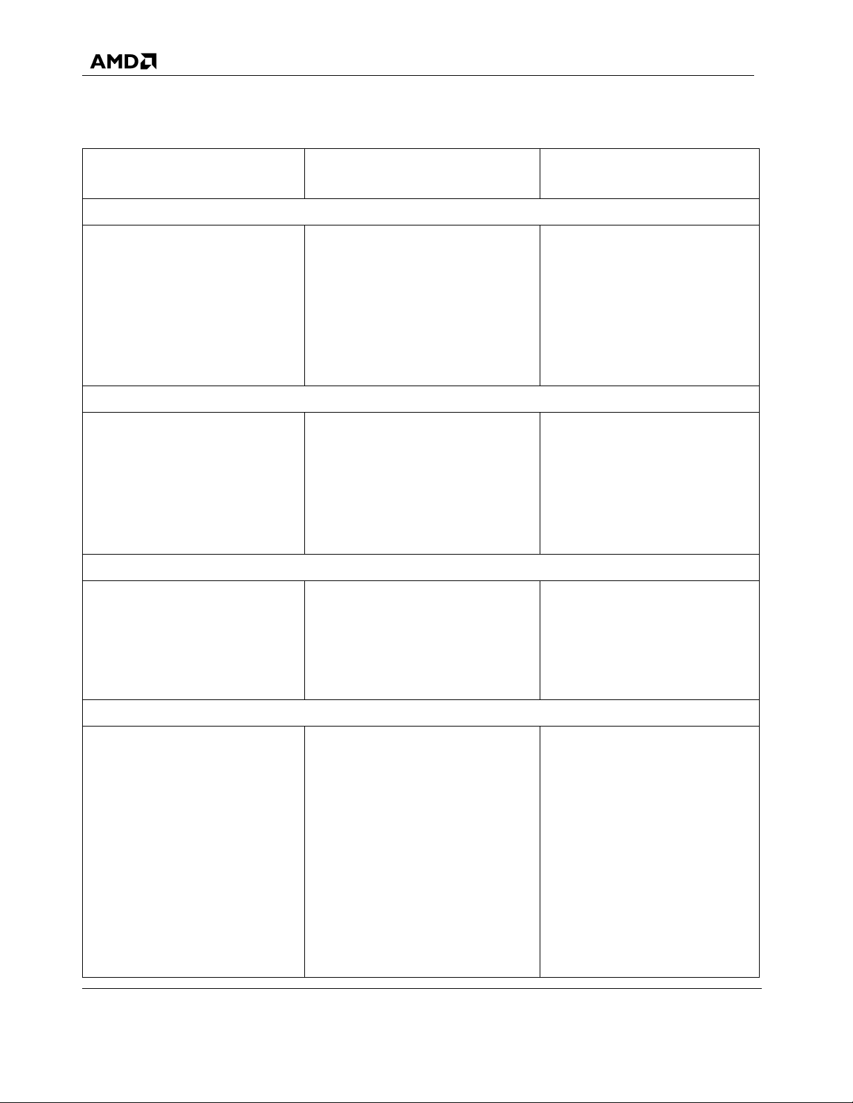
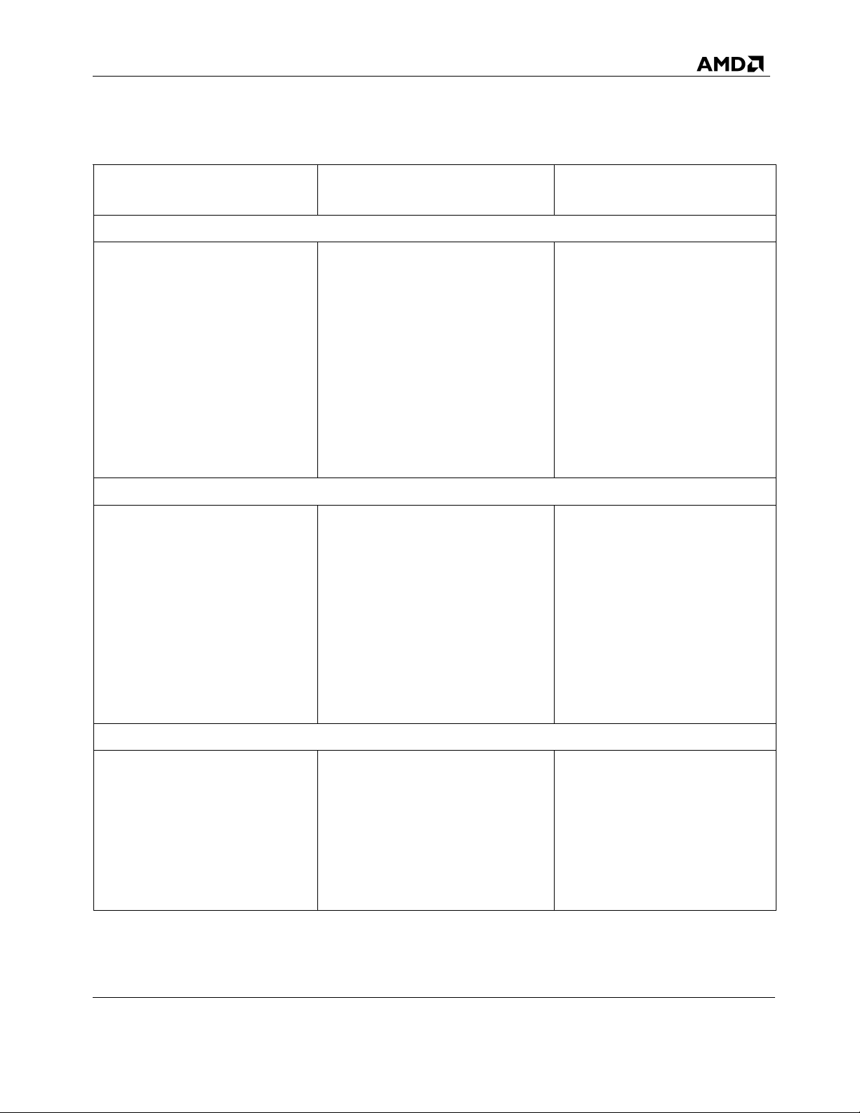
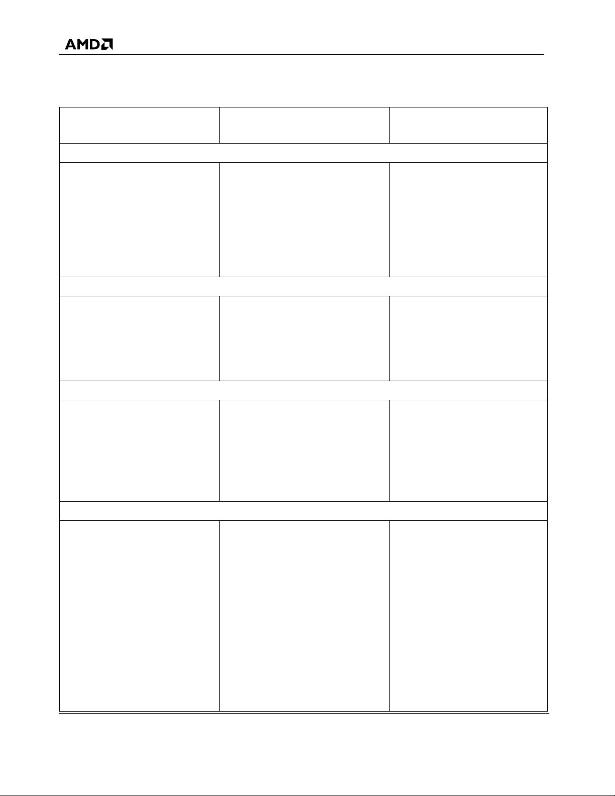
The test procedures, conditions, and requirements, for mechanical and environmental tests of the
Socket 940 are described in Table 1.
Table 1. Mechanical Qualification Test Descriptions
Procedures Conditions Requirements
Thermal Shock
EIA 364-32C Cold Extreme: –55°C, +0°C, –3°C
Hot Extreme: +110 °C, +3 °C,
–0 °C
Measure the dwell for 30 minutes
at each temperature extreme,
10 cycles, ≤ 15 seconds transition
time.
Group 2 samples exposed to the
environment while mated
Group 3 samples exposed to the
environment while unmated
Cyclic Humidity
EIA 364-31, Method III
Temperature: 25°C to 85°C
Relative Humidity: 90% to 95 %
1000 hours duration, 8 hours cycle
time.
Group 2 samples exposed to the
environment mated
Group 3 samples exposed to the
environment unmated
Visual Inspection—No physical
damage to socket housing or
contacts.
LLCR—25 mΩ max per contact
with Fe-Ni-Co alloy pin.
Visual Inspection—No physical
damage to socket housing or
contacts.
LLCR—25 mΩ max per contact
with Fe-Ni-Co alloy pin;
Measurements made at 250, 500,
750, and 1000 hours.
Chapter 4 Mechanical and Environmental Test Procedures, Conditions, and
Requirements
17
Page 18
AMD Socket 940 Qualification Plan
Table 1. Mechanical Qualification Test Descriptions (Continued)
Procedures Conditions Requirements
Thermal Cycling
30353 Rev. 3.04 September 2003
EIA 364-32
EIA 364-17, Method A
EIA 364- 17
Cold Extreme: –55°C, 20 minutes
dwell
Hot Extreme: 110°C, 15 minutes
dwell
1000 cycles, average rate of
temperature change between hot
and cold extremes must not be
greater than 10ºC per minute.
Temperature Life
Temperature: 115°C ± 2°C
500 hours duration
Preconditioning Thermal Aging
Temperature: 85°C ± 2°C
24 hours duration
Visual Inspection—No physical
damage to socket housing or
contacts.
LLCR—25 mΩ max per contact
with Fe-Ni-Co alloy pin;
Measurements made every 250
cycles.
Visual Inspection—No physical
damage to socket housing or
contacts
LLCR—25 mΩ max per contact
with Fe-Ni-Co alloy pin
Measurements made every 250
hours.
Visual Inspection—No physical
damage to socket housing or
contacts.
LLCR—Initial - less than 25 mΩ
per contact with Fe-Ni-Co alloy
pin.
Industrial Mixed Flowing Gas
EIA 364- 65, Condition IIA Chlorine—10 ppb
Hydrogen Sulfide—10 ppb
Nitrogen Dioxide—200 ppb
Sulfur Dioxide—100 ppb
Temperature: 30°C
Relative Humidity—70 %
Duration—First 5 days: one half of
the samples are mated and one half
of the samples are unmated.
Next 5 days—all samples mated.
Visual Inspection—No physical
damage to socket housing or
contacts.
LLCR—25 mΩ max per contact
with Fe-Ni-Co alloy pin;
Measurements made at 5 days
and at 10 days.
18 Mechanical and Environmental Test Procedures, Conditions, and
Requirements
Chapter 4
Page 19
30353 Rev. 3.04 September 2003
AMD Socket 940 Qualification Plan
Table 1. Mechanical Qualification Test Descriptions (Continued)
Procedures Conditions Requirements
Mechanical Shock
EIA 364-27, Test Condition A Tested with up to 900 grams
heatsink (and fan), attached with
assembly hardware to mated
package and socket with the PCB
retention mechanism.
50 G peak amplitude, 11 ms
duration, half-sine waveform.
3 shocks per direction, 3 axis—18
shocks total.
20 continuity circuits per test
sample must be monitored during
mechanical shock testing.
Random Vibration
EIA 364,-28, Test Condition VII Tested with up to 900 grams
heatsink (and fan), attached with
assembly hardware to mated
package and socket with the PCB
retention mechanism.
3.1 G rms, 20 to 500 Hz.
45 minutes duration per axis, 3 axis
total.
20 continuity circuits per test
sample must be monitored during
Random Vibration testing.
Visual Inspection—No physical
damage to socket housing or
contacts.
Continuity—No contact
discontinuity greater than 10 ns
duration.
LLCR—25 mΩ max per contact
with Fe-Ni-Co alloy pin.
Visual Inspection—No physical
damage to socket housing or
contacts.
Continuity—No contact
discontinuity greater than 10 ns
duration.
LLCR—25 mΩ max per contact
with Fe-Ni-Co alloy pin.
Durability
EIA 364-9 Initial actuation/de-actuation cycles
must be made by exercising five
cycles per µPGA package. The
final five cycles must be mated to
the actual µPGA package test
device.
Visual Inspection—No physical
damage to socket housing or
contacts.
LLCR—25 mΩ max per contact
with Fe-Ni-Co alloy pin.
Group 2—50 cycles per socket.
Group 5—5 cycles per socket.
Chapter 4 Mechanical and Environmental Test Procedures, Conditions, and
Requirements
19
Page 20
AMD Socket 940 Qualification Plan
Table 1. Mechanical Qualification Test Descriptions (Continued)
Procedures Conditions Requirements
Low Level Circuit Resistance (LLCR)
30353 Rev. 3.04 September 2003
EIA 364-23 100 mA maximum current, 20 mV
open circuit voltage.
Each measurement must be made
across a set of two daisy-chained
contact/pin locations.
200 daisy-chained circuits (400
µPGA socket contacts) must be
measured per mated test sample.
Dielectric Withstanding Voltage (DWV)
EIA 364- 20 650 VAC for 60 seconds.
25 contacts, randomly selected,
equally distributed throughout the
unmated socket; measurements
must be made with adjacent lateral,
diagonal and vertical contacts.
Insulation Resistance
EIA 364-21 100 VDC for 2 minutes.
25 contacts, randomly selected,
equally distributed throughout the
unmated socket;
The measurement must be made
with adjacent lateral, diagonal and
vertical contacts.
Initial LLCR must be less than
25 mΩ per contact with Fe-NiCo alloy pins.
After any reliability testing, final
LLCR must be less than 25 mΩ
per contact with Fe-Ni-Co alloy
pin.
No flashover or breakdown.
1000 MΩ minimum.
Contact Current Rating
EIA 364-70, Method 2
Five adjacent rows by
approximately 31 columns of
contacts per socket must be tested
at 1.5 A.
The temperature must be measured
at a minimum of five contact
locations per socket, with at least
one sensor located at the middle of
the energized pin field to capture
the maximum expected contact
temperature.
Temperature measurements must
be made until steady-state
conditions have been established.
The maximum contact
temperature rise must be less
than 30°C due to Joule heating,
for contact mating with Fe-NiCo alloy pin.
20 Mechanical and Environmental Test Procedures, Conditions, and
Requirements
Chapter 4
Page 21
30353 Rev. 3.04 September 2003
AMD Socket 940 Qualification Plan
Table 1. Mechanical Qualification Test Descriptions (Continued)
Procedures Conditions Requirements
Plating Thickness
Plating Thickness
EIA 364-48
EIA 364-60 Test must be performed on 25
EIA 364-56 Socket must be subjected to four
EIA 364-11A Four solutions test. Visual Inspection—No physical
Gold and nickel-plating thicknesses
must be measured on contact
mating areas; 25 loose contacts.
Contact Porosity (Gold Mating Areas)
loose contacts.
Resistance to Solder Heat
convection solder reflow processes
for mounting the socket to the
PCB.
Resistance to Solvents
30 micro-inches Au minimum
over 50 micro-inches Ni
minimum.
Quantify gold porosity of contact
mating areas.
Visual Inspection—No physical
damage to socket housing; no
deterioration of markings on
socket cover.
Socket cover must meet flatness
requirements before and after
solder reflow processes.
damage to socket housing; no
deterioration of markings on
socket cover.
Contact Normal Force
Tests must be performed on 5
individual contacts over the
deflection range expected for
engaging the package pin to the
contact.
Additionally, contact gap must be
measured before and after
force/deflection tests.
Socket Retention Force
Socket retention force must be
measured by extracting the µPGA
package from the actuated socket
with the cam lever in the lock
position.
Force/Deflection curve must be
generated for five cycles on each
contact sample.
Record initial and final contact
gap.
Minimum required socket
retention force is 0.013 kgf per
contact/pin or 12.5 kgf for mated
940 pins package.
Chapter 4 Mechanical and Environmental Test Procedures, Conditions, and
Requirements
21
Page 22
AMD Socket 940 Qualification Plan
Table 1. Mechanical Qualification Test Descriptions (Continued)
Procedures Conditions Requirements
Solder Ball Shear Force
30353 Rev. 3.04 September 2003
The force required to shear off the
solder ball on the contact
assembled in the socket housing
must be measured for 20 contact
locations for each unmated,
unmounted socket sample.
Lever Actuation and De-Actuation Force
The lever force must be measured
for actuating and de-actuating the
socket for 5 mating cycles per
sample.
Dimensional Inspection
Physical dimensions must be
measured for conformance to AMD
requirements and supplier
drawings.
Metallurgical Analysis
Two samples from each test group
(samples with the highest increase
in LLCR) must be subjected to
metallurgical analysis to determine
the wear out of the mating surfaces
on the contact and the package pin.
Five sets of LLCR circuits per
sample (10 contact and pin
positions) exhibiting the highest
LLCR increase, must be examined
for wear out of the gold plating into
the nickel underplating,
Minimum required shear force is
0.75 kgf per solder ball.
Maximum allowable lever force
is 3.6 kgf.
All dimensions must be within
tolerance specified by AMD
requirements and supplier
drawings.
There must be no evidence of
gold plating wear out.
22 Mechanical and Environmental Test Procedures, Conditions, and
Requirements
Chapter 4
Page 23
30353 Rev. 3.04 September 2003
AMD Socket 940 Qualification Plan
Chapter 5 Electrical Qualification
Requirements
This chapter describes the electrical qualification requirements for the Socket 940.
5.1 Fixture for Electrical Qualification Testing
Test fixtures required to conduct the electrical qualification requirements are furnished by AMD
directly to the AMD-designated test laboratory.
5.2 Electrical Specifications
Table 2 contains the summary of the electrical parameter specifications for the AMD µPGA
socket. The specifications do not include the effects of the fixtures. Use proper calibration to deembed the parasitic contributions for the fixture of the specified electrical parameters.
Table 2. Summary of Required Electrical Measurements for Socket 940
Measured Quantity Definition Specified
Value(s)
Mated partial selfinductance of a
single pin.
Note: This is the
only quantity
in the
specification
that does not
need
measuring.
Values
obtained
from an
accurate
detailed 3D
EM field
solver model
are
acceptable.
Mated loop
inductance of two
nearest pins (i.e.,
pins separated by
shortest distance).
Partial self
inductance of a
single-mated
(interposer-socket
combination) pin
calculated by
using a 3D EM
field solver.
The inductance of
a loop formed by
two nearest mated
pins. All current
is injected in one
pin and returned
through the other.
4nH maximum
assuming the
current return at
infinity.
3nH ± 10%
Measurement Applicable Standard
This quantity cannot be
measured directly nor be
calculated uniquely
from the measurements.
The inductance of a loop
formed by two nearest
pins, which are shorted
at the bottom of the
socket, with current
injected into one pin and
returned through the
other.
See Section 5.3.2 on page
27 for the discussion on the
mated partial selfinductance.
Use a validated “industrystandard” 3D EM field
solver.
This computed quantity
must not be used in any
calculations involving
measured data.
See Section 5.3.2 on page
27 for specified pin
configurations.
Chapter 5 Electrical Qualification Requirements 23
Page 24
[
]
AMD Socket 940 Qualification Plan
30353 Rev. 3.04 September 2003
Table 2. Summary of Required Electrical Measurements for Socket 940 (Continued)
Measured Quantity Definition Specified
Value(s)
Mated partial loop
i ductan e matrix n c
partial
L of three
loop
neighboring pins.
Mated capacitance
between two nearest
pins (i.e., pins
separated by
shortest distance).
Mated capacitance
matrix of three
neighboring pins.
The matrix is
defined as the
Maxwell (not
circuit) capacitance
matrix.
Differential
impedance between
two nearest pins
(i.e., pins separated
by shortest
distance).
Partial inductance
matrix of a mated
three-pin
combination
extracted from
mated two-pin
loop inductance
measurements.
One of the pins is
used as the
reference (current
return).
The capacitance
between two
nearest mated
pins.
The capacitance
matrix of three
neighboring pins
that are in the
same pattern as
those used to
extract the mated
partial inductance
matrix.
The transmission
line impedance of
the odd mode for
three mated pins,
using one pin as
the
voltage/current
reference.
L ≤ 3nH ±
loop
10%
These are the
diagonal entries
in the partial
loop inductance
matrix.
< 2nH ±
M
12
10%. These are
the off-diagonal
entries in the
partial loop
inductance
matrix.
1.0 pF max
All entries in the
matrix should
not exceed 1pF.
100 Ω ± 10%,
with an
additional ±
2Ω measurement
error.
Measurement Applicable Standard
The partial inductance
matrix is extracted from
a series of two-pin loop
inductance
measurements (as
described above) for
specified three-pin
configurations.
Capacitance between
two nearest pins
measured from the top
or bottom side of the
socket. Do not short
pins together for this
measurement.
The Maxwell
capacitance matrix
measured for the
specified mated threepin configurations. Do
not short pins together
for this measurement.
The differential (or an
odd mode) impedance
measured for a three-pin
configuration (S1, S2,
G).
If equipment permits,
measure this quantity
directly. If not,
calculate from the
measured, mated partial
loop inductance and
Maxwell capacitance
matrices according to
equations provided in
this document.
See Section 5.3.2 on page 27
for the definition of this
matrix and the measurements
that should be used to backcalculate the self and mutual
partial loop inductances.
Use the formulas provided in
Section 5.3.4.1 on page 28,
Equation (1).
Use the EIA-364-30 standard
for low frequency (10MHz)
measurements. Or, use the
network analyzer for Sparameter measurements
with minimum frequency of
500MHz or lower. See
Section 5.4 on page 29 for
test procedures.
Use the EIA-364-30 standard
for low frequency (10MHz)
measurements. Or, use the
network analyzer for Sparameter measurements
with minimum frequency of
500MHz or lower. See
Section 5.4 on page 29 for
test procedures.
Use the EIA-364-108
standard or see the equations
in terms of partial inductance
and Maxwell capacitance
matrices in Section 5.4 on
page 29.
If the time domain method is
used in measurement, then
the signal should have rise
time of 35ps to 150ps for
signal amplitude to go from
10% to 90%.
24 Electrical Qualification Requirements Chapter 5
Page 25
30353 Rev. 3.04 September 2003
AMD Socket 940 Qualification Plan
Table 2. Summary of Required Electrical Measurements for Socket 940 (Continued)
Measured Quantity Definition Specified
Value(s)
Propagation delay
skew among singleended signals.
Propagation delay
skew among
differential signal
pairs.
Deviation in the
propagation delay
skew of a singleended signal
through different
mated (single)
pins in the socket.
Deviation in the
propagation delay
of differential
signals through
mated pin pairs in
the socket.
10 ps max., plus
3 ps max.
measurement
error.
10 ps max plus 3
ps max
measurement
error.
Measurement Applicable Standard
Time delay of singleended signal between
the top pads of the
interposer and the pads
on the bottom side
fixture.
Locate the ground return
for the specified signal
pin pattern of singleended signals as
specified.
Time delay of a
differential signal
between the top pads of
the interposer and the
pads on the bottom side
of the fixture. The
specified three-pin (S1,
S2, G) arrangement
should be used.
Use EIA-364-103 standard or
Test Procedure in Section
5.6 on page 31.
Figure 2 on page 26 for
See
specified signal pin patterns,
which also include the
location of the current return
pin.
Use EIA-364-103 standard or
test procedure in Section 5.6
on page 31.
Figure 2 on page 26 for
See
specified differential pin-pair
patterns, which also include
the location of the current
return pin.
Frequencies for the
inductance
measurements.
Frequencies for the
capacitance
measurements.
The frequencies at
which inductance
is to be measured.
The frequencies at
which capacitance
is to be measured.
500 MHz and 2
GHz
500 MHz and 2
GHz
Any frequency domain
test equipment
recommended in EIA
standards may be used
to perform the
measurements. If time
domain equipment is
used, it should have
sufficient sampling rates
to resolve the specified
frequencies.
Any frequency domain
test equipment
recommended in EIA
standards may be used
to perform the
measurements. If time
domain equipment is
used, it should have
sufficient sampling rates
to resolve the specified
frequencies.
Chapter 5 Electrical Qualification Requirements 25
Page 26
[
]
[
]
[
]
AMD Socket 940 Qualification Plan
30353 Rev. 3.04 September 2003
Table 2. Summary of Required Electrical Measurements for Socket 940 (Continued)
Measured Quantity Definition Specified
Value(s)
Crosstalk between
nearest single-ended
and differential
signals.
This quantity should
be reported and
should serve as an
accuracy check for
the partial loop
inductance
and the Maxwell
capacitance
matrices.
partial
L
loop
Crosstalk is
defined as the
voltage (and
current) induced
on quiet (nondriven)
transmission lines
(single-ended or
differential) due
to the nearest
driven (singleended or
differentially
driven) neighbors.
Crosstalk should
be measured and
compared to the
results predicted
from the
measured
partial
L and
loop
Maxwell
capacitance
matrices.
Measurement Applicable Standard
Measurements are to be
performed for specified
pin patterns that will
include, at least, the
nearest and next to
nearest neighbors.
Use EIA-364-90 standard—
Method A or Method B for
pin patterns specified in
Figure 2 on page 26.
See Section 5.7 on page 33
for the definitions of
crosstalk in terms of the
elements of the measured
partial
L and capacitance
loop
matrices.
5.3 Inductance Measurements
This section describes the capacitance and inductance matrices, the mated partial self inductance,
mated loop inductance, and the mated partial loop inductance matrix.
5.3.1 Capacitance and Inductance Matrices
Measure the partial loop inductance and Maxwell capacitance matrices for the three mated-pin
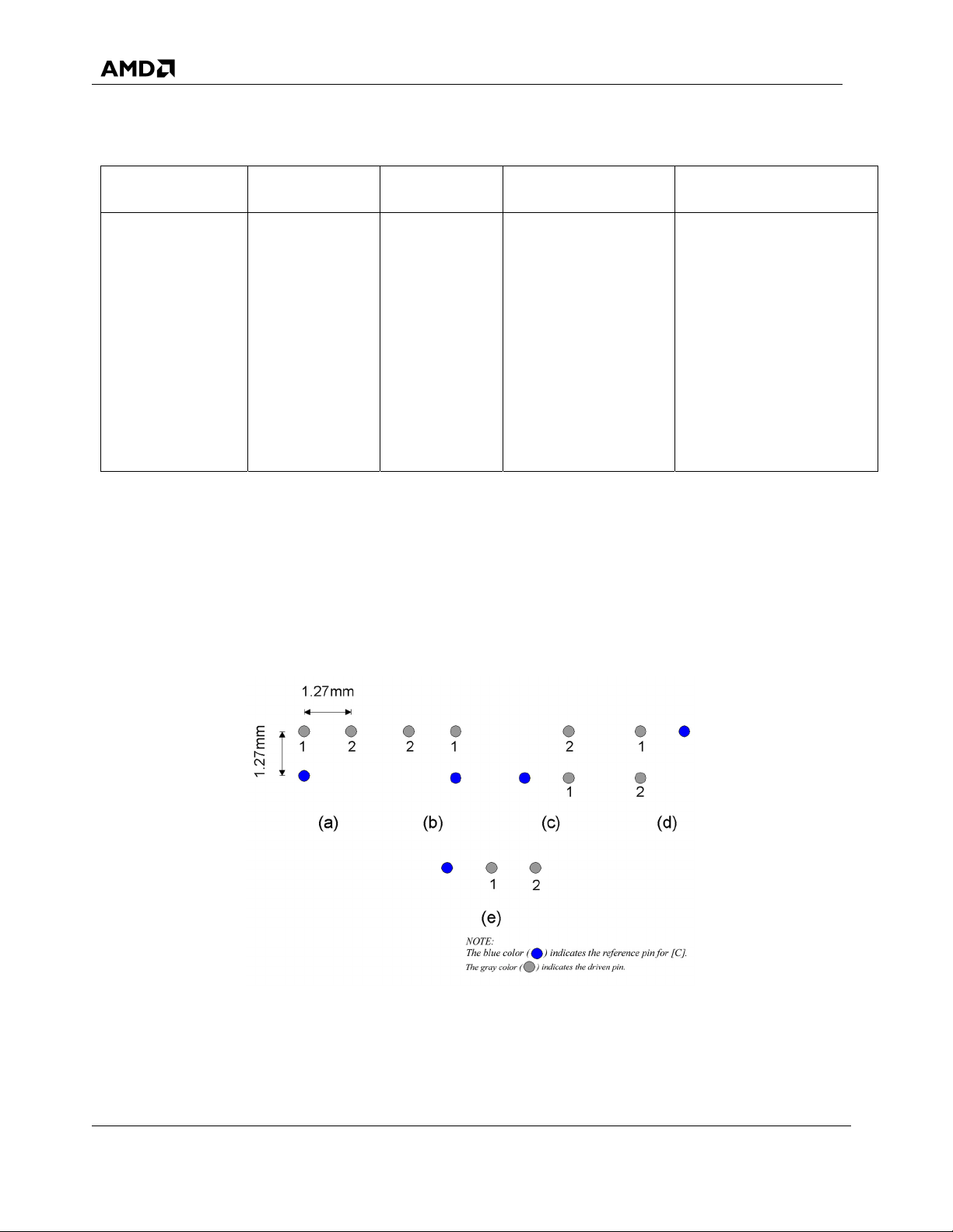
configurations shown in Figure 2.
Figure 2. Pin Configurations for the Maxwell Capacitance and Partial Inductance Matrix
Measurement
For the pin configurations shown in Figure 2, the size of the Maxwell capacitance matrix is 2x2,
which is also the size of the partial loop inductance matrix.
26 Electrical Qualification Requirements Chapter 5
Page 27

30353 Rev. 3.04 September 2003
AMD Socket 940 Qualification Plan
5.3.2 Mated Partial Self-Inductance
The following sections are procedures required to properly test for mated partial self-inductance.
5.3.2.1 Test Procedure
Use a validated
industry-standard 3-D EM field solver. This is the only quantity in the
specification that need not be measured. Values obtained from an accurate detailed 3-D EM field
solver model are acceptable. Do not use this computed quantity in any calculations involving
measured data.
5.3.2.2 Test Condition
• Test Frequencies are 500 MHz and 2 GHz.
• Use a validated
industry standard 3-D EM field solver.
• The computed data is not used in any calculations involving measured data.
5.3.2.3 Requirements
Mated partial self-inductance is 4 nH maximum, assuming the current return is at infinity.
5.3.3 Mated Loop Inductance
The following sections are procedures required to properly test for mated loop inductance.
5.3.3.1 Test Procedure
The loop inductance is formed by a pair of pins. All current is injected in one pin and returned
through the other. On a vector network analyzer using one port measurement, read the values
from the Smith chart at the specified frequencies.
5.3.3.2 Test Condition
• Test Frequencies are 500 MHz and 2 GHz
• See Figure 2 on page 26 f or pin placement.
5.3.3.3 Requirements
Mated Loop Inductance must be 3 nH ± 10%—two nearest pins, current in one pin, return from
the other pin. Record all pin pattern readings, but use only the nearest neighbors for qualification.
5.3.4 Mated Partial Loop Inductance Matrix
The following sections are procedures required to properly test for mated partial loop inductance
from measured mated-loop inductance data.
Chapter 5 Electrical Qualification Requirements 27
Page 28
AMD Socket 940 Qualification Plan
30353 Rev. 3.04 September 2003
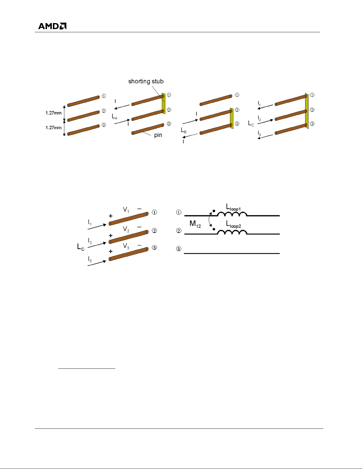
Figure 3 shows the loop measurement for extracting [Lp] for a mated three-pin combination.
Figure 3. Loop Measurements for Extracting [Lp] for a Mated Three-Pin Combination
Figure 4 shows the current/voltage definitions and equivalent circuit of the partial loop inductance
matrix.
Figure 4. Current/Voltage Definitions and Equivalent Circuit of the Partial Loop Inductance
Matrix
5.3.4.1 Test Procedure
As shown in Figure 3, the partial inductance matrix of a mated three-pin combination that is
extracted from a mated two-pin loop inductance measurement with one of the pins used as the
reference (current return). Use the formula in Equation (1) to calculate the mated partial loop
inductance from measured mated loop inductance data.
LLL
−+
321
M
=
12
2
looplooploop
(1)
5.3.4.2 Test Condition
Test Frequencies are 500 MHz and 2 GHz.
28 Electrical Qualification Requirements Chapter 5
Page 29

30353 Rev. 3.04 September 2003
5.3.4.3 Requirements
• M < 2 nH ± 10%—three pin loop with one pin used as reference.
• Measurement of the off diagonal entries in the loop partial inductance matrix.
• Diagonal entries of this matrix correspond to mated loop inductance and must meet specified
values in Section 5.3.3.3 on page 27.
AMD Socket 940 Qualification Plan
5.4 Capacitance Measurements
At low frequencies, the measurement of the capacitance should be carried out according to the
EIA Standard 364-30. Two types of measurements are required; the single capacitance between
the two nearest pins that are separated by 1.27mm and the Maxwell capacitance matrix for
multiple pins.
5.4.1 Test Procedures
Use the procedures shown in EIA-364-30 and Section 5.3.2.
5.4.2 Test Condition
Test Frequencies are 500 MHz and 2 GHz.
Note: Do not short pins for this test.
The matrix is defined as the Maxwell (not circuit) capacitance matrix.
5.4.3 Requirements
• The mated capacitance of any two adjacent pins is 1 pF maximum, measured from the top or
bottom of the socket.
• The mated capacitance matrix of three neighboring pins is 1 pF maximum.
• The Maxwell capacitance matrix is measured for a specified mated three-pin configuration.
• The capacitance matrix of three neighboring pins that are in the same pattern as those used to
extract the mated partial inductance matrix.
5.5 Differential Impedance
If the dimensions of the socket pins and the spacing between them are small compared to the
wavelength of the highest frequency component of interest, then the impedance of the three-pin
configuration shown in Figure 2 on page 26 and Figure 4 on page 28, can be calculated
approximately from the lumped loop inductance and Maxwell capacitance matrices. When pins 1
Chapter 5 Electrical Qualification Requirements 29
Page 30
[
]
AMD Socket 940 Qualification Plan
30353 Rev. 3.04 September 2003
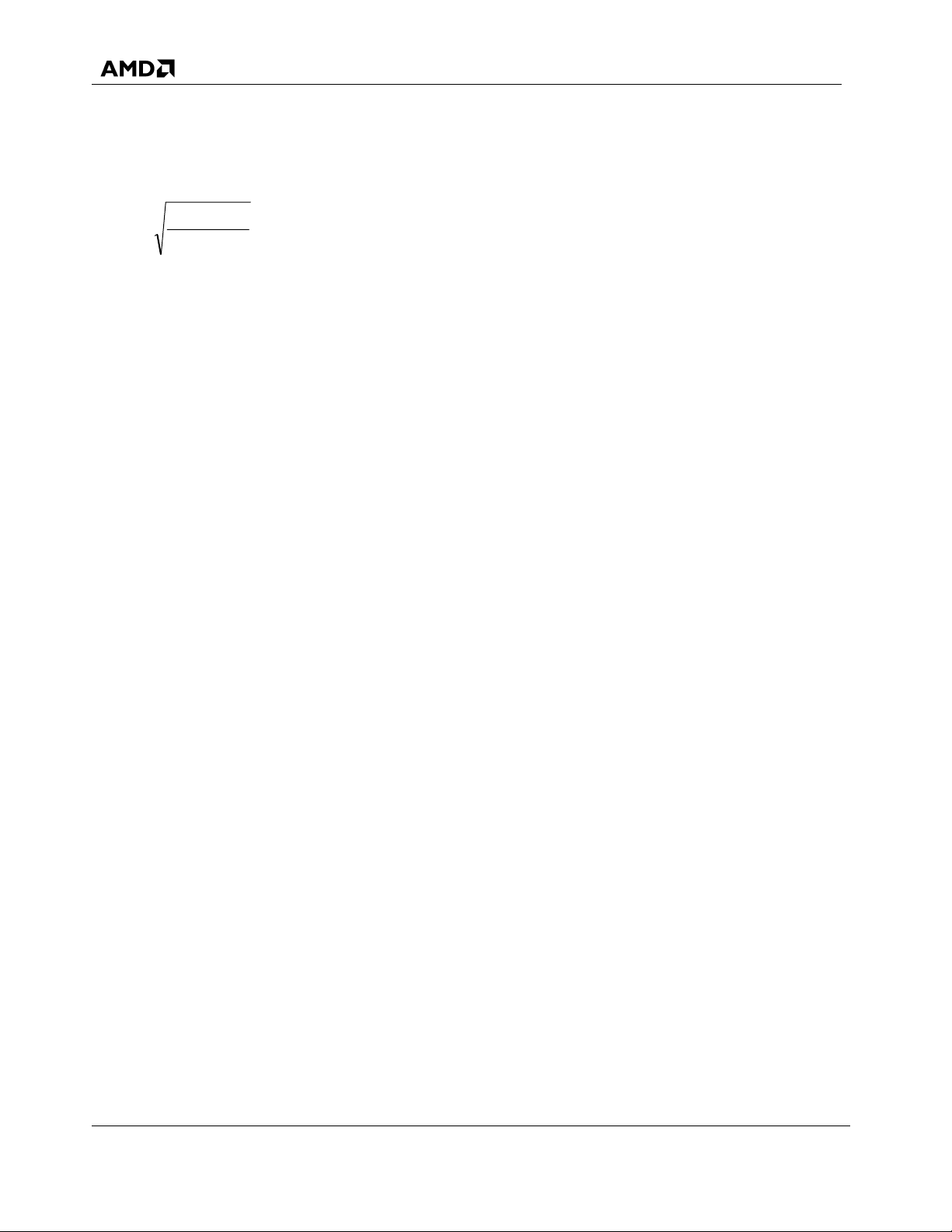
and 2 in Figure 4 on page 28 are driven differentially, with pin 3 acting as ground, then the
differential impedance of the transmission line formed by this pin configuration is given by
ML
−
Z
diff
loop
= * 2. (2)
12
CC
+
12
The definition in Equation (2) for the differential impedance assumes that the driven (or signal)
conductors have the same geometrical shape.
Note: Equation (2) is only valid for non-symmetric differential lines in homogeneous media.
The differential impedance should be measured for all combinations of the three-pin arrangements
shown in Figure 2 on page 26. The pins are intentionally numbered in a specific manner so as to
[
yield identical
L and
loop
]
matrices for pin configurations (a) through (d) in Figure 2 on page
C
26. This is not the case for the pin arrangement (e) in Figure 2 on page 26.
5.5.1 Differential Impedance Measurement
The following sections are procedures required to properly test for Differential Impedance.
5.5.1.1 Test Procedure
• Use the procedures shown in EIA-364-108 or see the equations in terms of partial loop
inductance and Maxwell capacitance matrices. If the time domain method is used in
measurements, then the signal should have rise time of 35 to 150 ps for signal amplitude to go
from 10 to 90%.
• Measure the differential transmission line impedance for three mated pins, using one pin as the
voltage/current reference.
• Any frequency domain test equipment recommended in EIA-364-108 may be used to perform
the measurements.
• If time domain equipment is used, it should have sufficient sampling rates to resolve the
specified frequencies.
5.5.1.2 Test Condition
• Frequency or time domain method.
• Time domain method uses a rise time of 35 to 150 ps for signal amplitude to go from 10 to
90%.
• Frequency domain method measurements made at 500 MHz and 2 GHz.
• The differential impedance measured for a three-pin configuration (S1, S2, G).
30 Electrical Qualification Requirements Chapter 5
Page 31
30353 Rev. 3.04 September 2003
AMD Socket 940 Qualification Plan
5.5.1.3 Requirements
The acceptable range for the differential impedance is 100 ± 10% Ω with an additional ± 2 Ω
measurement error.
5.6 Propagation Delay Measurements
This section describes the propagation delay skew for single-ended signal pins and the differential
propagation delay skew.
5.6.1 Single-Ended Propagation Delay Skew
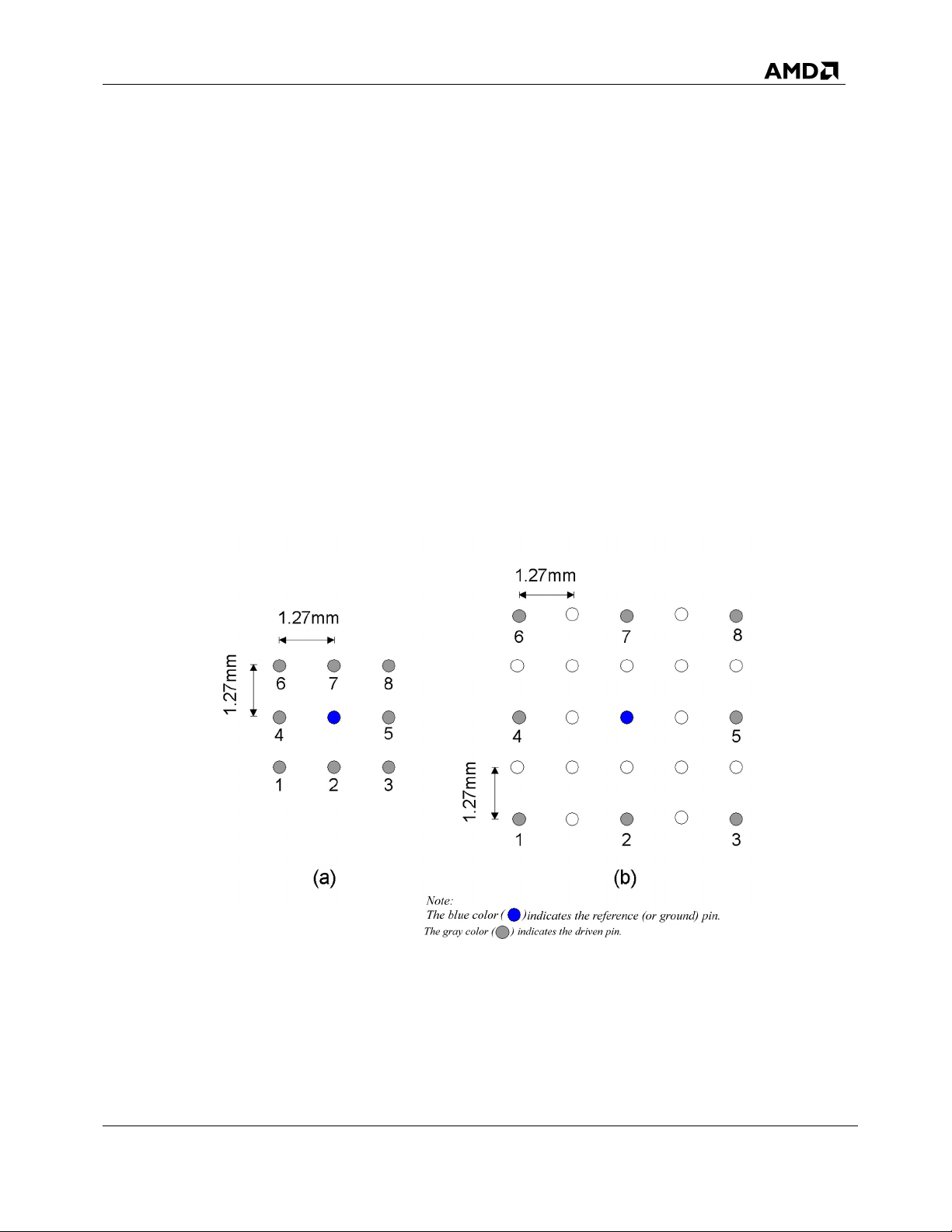
The propagation delay skew for single-ended signal pins is to be measured for the pin
configurations shown in Figure 5
Figure 5. Pin Configurations for the Propagation Delay Skew Measurements of
Single-Ended Signals
Each measurement must consist of driving one (gray-shaded) pin as signal and using the center pin
(blue) as return. The propagation delay for all signal pins in Figure 5(a) must be measured. The
maximum allowable deviation for all the pins in the array must be less than the specified value.
An identical set of measurements must also be repeated for the pin array shown in Figure 5(b).
Chapter 5 Electrical Qualification Requirements 31
Page 32
AMD Socket 940 Qualification Plan
30353 Rev. 3.04 September 2003
5.6.1.1 Test Procedure
Use the procedures shown in EIA-364-103 for testing the single–ended propagation delay skew.
Propagation delay skew can also be measured using a time delay reflectometer (TDR) by
launching the signals through the designated pins, such as those in Figure 5 on page 31. The
signals are launched from the interposer and the delay skew is observed at the test board. The
difference in the propagation times (delay skew) through different pins in the socket can be clearly
seen and measured at the open circuited end of the test board.
5.6.1.2 Test Condition
For the time domain method:
Time delay of single-ended signals between the top pads of the interposer and the pads on the
bottom side fixture.
The ground return for the specified signal pin pattern of single-ended signals is to be located as
specified.
5.6.1.3 Requirements
• Deviation in the delay (skew) among the single-ended pins between the top of the package and
the PCB under the socket must be 10 ps maximum plus 3 ps maximum measurement error.
• Three pins S1, S2, and G should be used for this measurement.
5.6.2 Differential Propagation Delay Skew
The differential propagation delay skew must be measured for every pin configuration shown in
Figure 2 on page 26. In each measurement the two gray-shaded pins (denoted 1 and 2) must be
driven as signals in differential form, using the blue pin as ground. The maximum allowable
deviation in the propagation delay skew for all specified pin configurations must be less than the
specified value.
5.6.2.1 Test Procedure
Use the procedures shown in EIA-364-103 and Section 5.6.1.
5.6.2.2 Test Condition
For the time domain method:
Time delay of a differential signal between the top pads of the interposer and the pads on the
bottom side of the fixture.
32 Electrical Qualification Requirements Chapter 5
Page 33

30353 Rev. 3.04 September 2003
[
]
[
]
5.6.2.3 Requirements
• Deviation in the delay (skew) of a differential signal between the top of the package and PCB
under the socket must be 10 ps maximum plus 3 ps maximum measurement error.
• Three pins S1, S2, and G should be used for this measurement.
AMD Socket 940 Qualification Plan
5.7 Single-Ended and Differential Crosstalk
The following procedures are required to properly test for crosstalk.
5.7.1 Test Procedure
Use the procedures shown in EIA 364-90, Method A or B, for the definitions of crosstalk in terms
of the elements of the measured partial loop inductance
matrices.
partial
L and Maxwell capacitance
loop
5.7.2 Test Condition
• Frequency or time domain method
• For time domain method—use rise time 35 to 150 ps for signal amplitude to go from 10 to
90%
• For frequency domain method—use 500 MHz and 2 GHz
• Measurements performed for specified pin patterns, differential shown in Figure 2 on page 26
and single ended shown in Figure 5 on page 31, must include the minimum, the nearest, and
next to nearest neighboring pins.
5.7.3 Requirements
Crosstalk should be recorded and serve as an accuracy check for the partial loop inductance
partial
L and the Maxwell capacitance matrices.
loop
Chapter 5 Electrical Qualification Requirements 33
 Loading...