

Page 1
AMD Socket 940 Design
Specification
Publication #
Issue Date:
25766
September 2003
Revision:
3.03
Page 2

© 2002, 2003 Advanced Micro Devices, Inc. All rights reserved.
The contents of this document are provided in connection with Advanced
Micro Devices, Inc. (“AMD”) products. AMD makes no representations or
warranties with respect to the accuracy or completeness of the contents of this
publication and reserves the right to make changes to specifications and
product descriptions at any time without notice. No license, whether express,
implied, arising by estoppel, or otherwise, to any intellectual property rights
are granted by this publication. Except as set forth in AMD’s Standard Terms
and Conditions of Sale, AMD assumes no liability whatsoever, and disclaims
any express or implied warranty, relating to its products including, but not
limited to, the implied warranty of merchantability, fitness for a particular
purpose, or infringement of any intellectual property right.
AMD’s products are not designed, intended, authorized or warranted for use as
components in systems intended for surgical implant into the body, or in other
applications intended to support or sustain life, or in any other application in
which the failure of AMD’s product could create a situation where personal
injury, death, or severe property or environmental damage may occur. AMD
reserves the right to discontinue or make changes to its products at any time
without notice.
Trademarks
AMD, the AMD Arrow logo, AMD Athlon, AMD Opteron, and combinations thereof are trademarks of
Advanced Micro Devices, Inc.
Other product names used in this publication are for identification purposes only and may be trademarks of their
respective companies.
Page 3

25766 Rev. 3.03 September 2003
AMD Socket 940 Design Specification
Contents
Revision History.............................................................................................................................6
1 Introduction ...........................................................................................................................7
1.1 Purpose.............................................................................................................................7
1.2 Supplier Requirements.....................................................................................................7
2 Microprocessor Package Description ..................................................................................9
2.1 940-pin Ceramic µPGA Package .....................................................................................9
2.2 Package Substrate and Pin Dimensions. ........................................................................10
3 Socket Mechanical Requirements ......................................................................................11
3.1 Socket Outline................................................................................................................11
3.2 Package Seating Plane ...................................................................................................12
3.3 Socket Base and Cover ..................................................................................................12
3.3.1 Socket Markings ....................................................................................................12
3.4 Socket Contact ...............................................................................................................13
3.4.1 Contact Base Metal................................................................................................13
3.4.2 Contact Plating.......................................................................................................13
3.4.3 SMT Solder Balls...................................................................................................13
3.5 Socket Actuation Lever..................................................................................................13
3.5.1 Package Insertion and Extraction Force ................................................................13
3.5.2 Socket Retention Force..........................................................................................13
3.5.3 Locking Latch ........................................................................................................14
3.5.4 Lever Actuation and De-Actuation Force..............................................................14
3.5.5 Pin Field Actuation Displacement .........................................................................14
3.6 Socket Durability ...........................................................................................................14
Contents 3
Page 4

AMD Socket 940 Design Specification
25766 Rev. 3.03 September 2003
3.7 Visual Inspection...........................................................................................................14
3.7.1 Solder Balls ........................................................................................................... 14
3.7.2 Contacts................................................................................................................. 14
3.7.3 Cover and Base...................................................................................................... 14
3.7.4 Actuation Lever.....................................................................................................14
4 Socket Electrical Requirements.........................................................................................15
4.1 Contact Current Rating.................................................................................................. 15
4.2 Low Level Circuit Resistance (LLCR) ......................................................................... 15
4.3 Inductance ..................................................................................................................... 15
4.4 Capacitance ................................................................................................................... 16
4.5 Differential Impedance.................................................................................................. 16
4.6 Propagation Delay ......................................................................................................... 16
4.7 Crosstalk........................................................................................................................16
4.8 Dielectric Withstanding Voltage (DWV)...................................................................... 16
4.9 Insulation Resistance.....................................................................................................16
4 Contents
Page 5

25766 Rev. 3.03 September 2003
AMD Socket 940 Design Specification
List of Figures
Figure 1. A 3-D View of Socket 940. ...............................................................................................7
Figure 2. 940-Pin Ceramic µPGA Package Drawing ........................................................................9
Figure 3. Socket 940 Outline ..........................................................................................................11
List of Figures 5
Page 6
AMD Socket 940 Design Specification
25766 Rev. 3.03 September 2003
Revision History
Date Revision Changes
September 2003
3.03
Third public release.
September 2003
May 2003
April 2003
3.02
3.01
3.00
Internal revision.
Second public release.
Initial public release.
6 Revision History
Page 7
25766 Rev. 3.03 September 2003
AMD Socket 940 Design Specification
1 Introduction
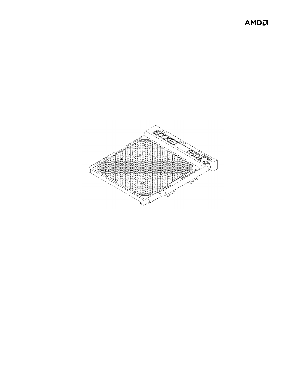
This document defines the requirements for a 940-pin, 1.27-mm pitch, surface mount technology
(SMT), zero insertion force (ZIF) socket (herein referred to as “Socket 940”) for use with
Advanced Micro Devices (AMD) 940-pin ceramic micro pin grid array (µPGA) package. Socket
940, shown in Figure 1, provides a reliable electrical interconnect between the printed circuit
board (PCB) and the 940 pins of the ceramic µPGA package, throughout the life of the product.
Figure 1. A 3-D View of Socket 940.
1.1 Purpose
This document specifies the dimensional, mechanical, electrical, and reliability requirements for
the Socket 940 that are necessary to meet the performance requirements of AMD Athlon™ 64 FX
processor or AMD Opteron™ processor products.
1.2 Supplier Requirements
To become an AMD qualified supplier for Socket 940, the potential socket supplier shall
demonstrate that their product meets the requirements listed in this document and by conducting
qualification testing on their production run sockets in accordance with the AMD Socket 940
Qualification Plan.
Chapter 1 Introduction 7
Page 8

AMD Socket 940 Design Specification
25766 Rev. 3.03 September 2003
8 Introduction Chapter 1
Page 9
25766 Rev. 3.03 September 2003
AMD Socket 940 Design Specification
2 Microprocessor Package Description
This chapter provides dimensional information for the 940-pin ceramic µPGA package that mates
with Socket 940.
2.1 940-pin Ceramic µPGA Package
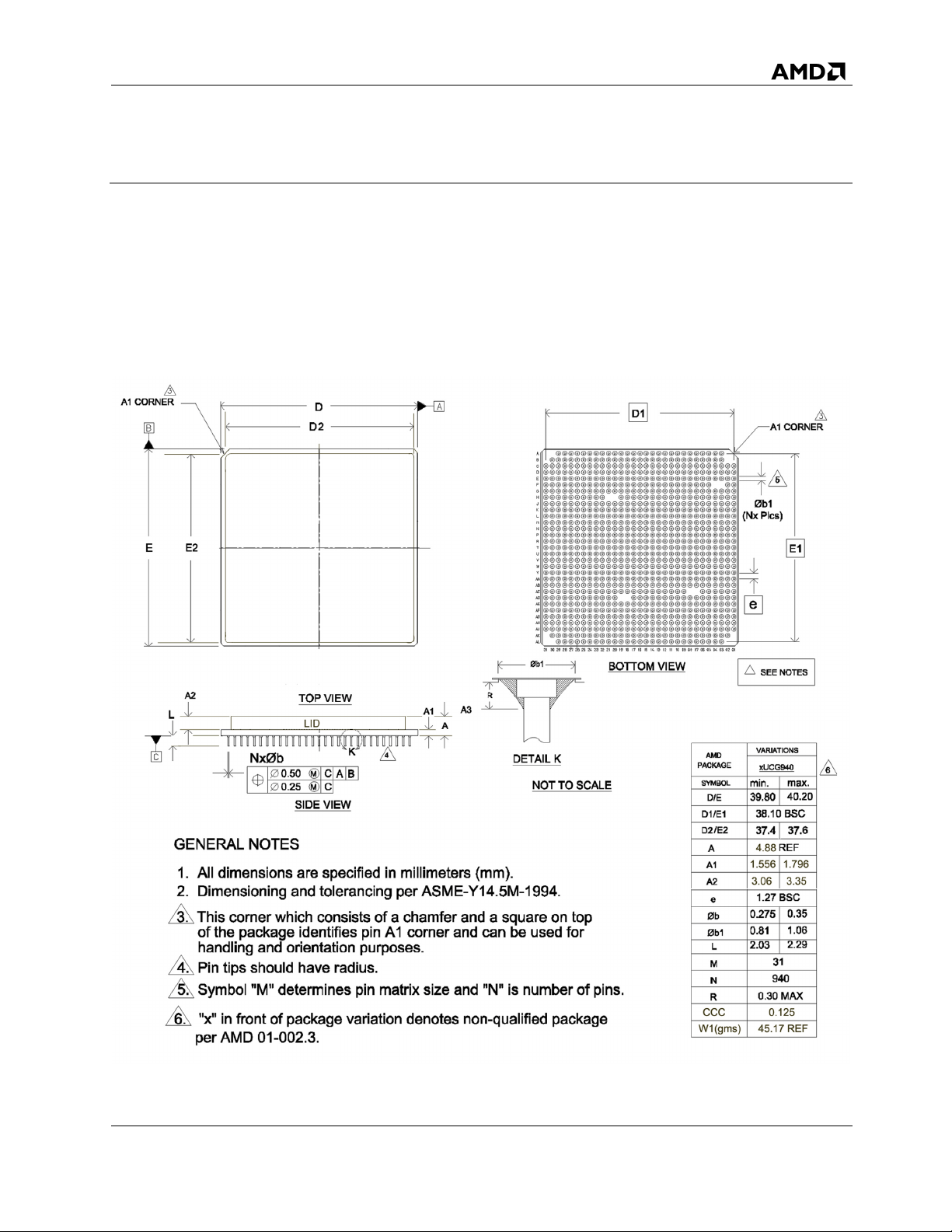
The 940-pin ceramic µPGA package drawing is shown in Figure 2.
Figure 2. 940-Pin Ceramic µPGA Package Drawing
Chapter 2 Microprocessor Package Description 9
Page 10

AMD Socket 940 Design Specification
25766 Rev. 3.03 September 2003
2.2 Package Substrate and Pin Dimensions.
The package substrate and pin dimensions, tolerances, and true position parameters are shown in
Figure 2 on page 9.
Socket 940 is designed to be functional with the lidded, as well as with the lidless package
configuration. The total package thickness for the lidless configuration is 2.20 mm minimum.
10 Microprocessor Package Description Chapter 2
Page 11
25766 Rev. 3.03 September 2003
AMD Socket 940 Design Specification
3 Socket Mechanical Requirements
This chapter discusses the socket outline and mechanical requirements for the Socket 940.
3.1 Socket Outline
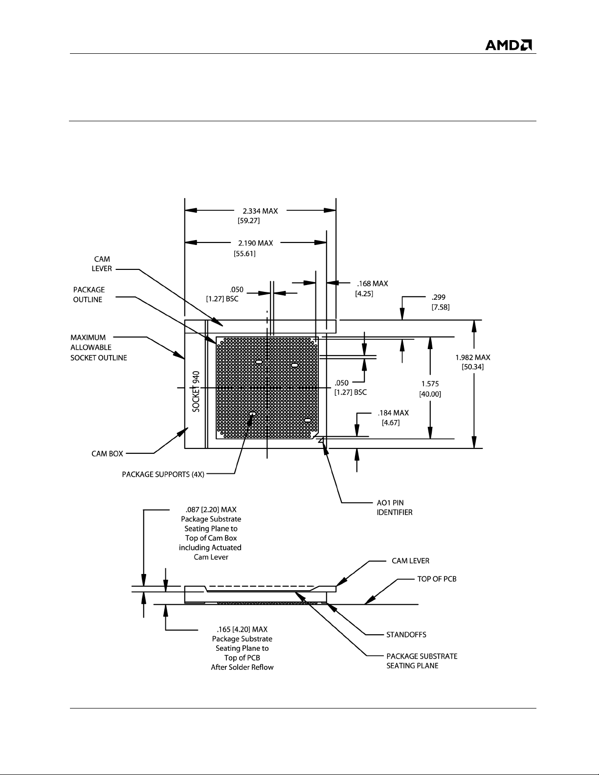
Figure 3 shows the allowable outline for the Socket 940. All dimensions shown are in millimeters.
Figure 3. Socket 940 Outline
Chapter 3 Socket Mechanical Requirements 11
Page 12

AMD Socket 940 Design Specification
25766 Rev. 3.03 September 2003
3.2 Package Seating Plane
The cover for the Socket 940 is designed to accommodate the package pin shoulder and
braze/solder fillet as shown by the 940-pin ceramic µPGA package drawings in Figure 2. Support
structures are incorporated into the socket cover to provide sufficient mechanical support (seating
plane) for the package substrate, without causing damage to the package pins at any time.
The package-seating plane on the socket cover has a surface flatness better than 0.25 mm, when
unmated as well as when mated with a package. After socket mounting to the printed circuit board
(PCB), the package-seating plane on the socket cover is 4.00 ± 0.20 mm from the mounting
surface of the PCB.
3.3 Socket Base and Cover
The socket base and socket cover are made from Liquid Crystal Polymer (LCP) with a UL
flammability rating of 94 V-0. The base color is black and the cover color is natural or ivory.
The thickness of the socket cover (including the 0.30 mm pocket recess) must not exceed 1.17
mm. The socket cover flatness is less than 0.25 mm, before and after the SMT reflow to the PCB.
The flatness measurement must remain less than 0.25 mm after environmental and mechanical
testing.
Either a removable tape or plastic cover acts as an overlay for the pin holes in the top of the socket
cover. The overlay facilitates socket pick-and-place operation with a vacuum nozzle during board
assembly. The overlay must not outgas during the solder reflow processes or leave any residue
upon removal prior to package pins insertion.
3.3.1 Socket Markings
The socket identifier marking “SOCKET 940” must be molded into the top surface of the socket
cover cam box region, where the number 940 represents the pin count of the mating ceramic
µPGA package (see Figure 1 on page 7).
A locked and unlocked directional designator is molded into the top surface of the cam box, in
close proximity to the actuation lever. See Figure 1 on page 7.
A triangular shape symbol must be molded into the top of the socket cover for proper package pin
A01 orientation. This orientation symbol is located to remain visible after the package is mated to
the socket as shown in Figure 1 on page 7 and Figure 3 on page 11.
The supplier’s UL approved symbol is molded on the socket cover. This marking is located such
that it remains visible and readable after the socket is solder mounted onto the PCB.
The lot traceability number can be ink, laser, or impact marked on the socket cover. This marking
must be located to be visible and readable after the socket is solder mounted onto the PCB.
12 Socket Mechanical Requirements Chapter 3
Page 13

25766 Rev. 3.03 September 2003
AMD Socket 940 Design Specification
3.4 Socket Contact
This section describes the contact material and solder balls for socket attachment to the PCB.
Note: No lubricants can be present on the contact mating areas of fully assembled sockets that
are shipped to customers by the supplier.
3.4.1 Contact Base Metal
The contact base metal is high-strength copper alloy.
3.4.2 Contact Plating
The entire contact is plated with 1.27-µm minimum thickness of nickel.
The contact mating area is plated with 0.76-µm minimum thickness of gold over the 1.27 µm
minimum thickness of nickel underplating.
3.4.3 SMT Solder Balls
The socket is mounted to the PCB by SMT, with a PCB solder pad diameter of 0.64 mm.
Each solder ball on the socket is tin and lead (63/37 ± 5%) with a diameter of 0.76 mm.
The contact must include a solder barrier feature to prevent solder from wicking up into the
contact mating area during solder reflow.
The Socket 940 solder ball field must meet the co-planarity requirement of 0.20 mm.
3.5 Socket Actuation Lever
The socket incorporates a stainless steel lever to the right side of the cam box for actuating and deactuating the socket contacts with the package pins. This actuation lever provides the mechanical
advantage to easily actuate the socket in an OEM high-volume manufacturing environment and
also facilitates toolless socket actuation and de-actuation operations by the end-user.
3.5.1 Package Insertion and Extraction Force
With the actuation lever in the open position, the package insertion and extraction forces,
conceptually, are zero. These insertion and extraction forces must not exceed 2 kgf in actual
applications.
3.5.2 Socket Retention Force
With the actuation lever in the closed position, the force required to extract the package pins out of
the socket contacts must be a minimum of 0.013 kgf per pin.
Chapter 3 Socket Mechanical Requirements 13
Page 14

AMD Socket 940 Design Specification
25766 Rev. 3.03 September 2003
3.5.3 Locking Latch
The socket cover incorporates a latch mechanism to lock the lever in the closed position after the
socket contacts are mated with the package pins. Support tab(s) are added to the socket cover to
cradle the actuation lever in the closed position. The tab(s) prevent the actuation lever from
contacting the PCB.
3.5.4 Lever Actuation and De-Actuation Force
The force required to actuate or de-actuate the lever must be less than 3.6 kgf.
3.5.5 Pin Field Actuation Displacement
The package pins must be displaced less than 1.0 mm during socket actuation or de-actuation.
3.6 Socket Durability
The socket must maintain electrical and mechanical integrity after 50 actuation and de-actuation
cycles.
3.7 Visual Inspection
All visual inspections shall be at 1X magnification, except for solder balls, which must be
inspected at 5X magnification.
3.7.1 Solder Balls
There can be no missing, malformed, damaged, or misaligned solder balls attached to the contacts.
3.7.2 Contacts
There can be no missing or damaged contacts that prevent the socket from functioning properly.
Contact mating surface must not be missing gold plating.
3.7.3 Cover and Base
There can be no cracks or flashing visible on the socket cover and base. All tabs for securing the
socket cover to the base must not be damaged or missing. The socket cover must fit properly on
the socket base with no visible gap between them. The lever latch cannot be damaged or
malformed.
3.7.4 Actuation Lever
The actuation lever cannot be damaged, malformed, or missing.
14 Socket Mechanical Requirements Chapter 3
Page 15

25766 Rev. 3.03 September 2003
AMD Socket 940 Design Specification
4 Socket Electrical Requirements
This chapter describes the contact current rating, inductance, capacitance, differential impedance,
propagation delay, crosstalk, dielectric withstanding voltage, and insulation resistance of the
Socket 940.
4.1 Contact Current Rating
The contact must be rated at a current rating of 1.5 A per contact, with less than 30°C temperature
rise with a minimum of six rows of mated contacts and pins energized.
4.2 Low Level Circuit Resistance (LLCR)
Contact resistance applies to the mounted socket with actuated package pin, and includes the bulk
resistance of the contact, solder ball, package pin, and the interface resistance between the contact
and the package pin, but does not include the package internal trace resistance.
Initial Circuit Resistance
Initial circuit resistance shall be measured immediately after the first mating of the package pins to
the socket contacts. Two hundred daisy-chained pairs (400 contact locations) must be measured
per socket sample. Initial LLCR must not exceed 25 mΩ per contact when mated with Kovar
pins, based on measurements made on a daisy-chained pair of contacts.
Final Circuit Resistance
Final circuit resistance shall be measured after the mechanical and environmental testing of the
mated package and socket is complete. The same 200 daisy-chained pairs (400 contact locations)
must be measured per socket sample. Final LLCR must not exceed 25 mΩ per contact when
mated with Kovar pins, based on measurements made on a daisy-chained pair of contacts.
4.3 Inductance
The mated, partial self-inductance of a single pin must be less than 4 nH.
The mated-loop inductance of two nearest pins must be 3 nH ± 10%.
The mated partial-loop inductance matrix of three neighboring pins must be 3 nH ± 10%.
Note: Measurements are made at frequencies of 500 MHz and 2 GHz.
Chapter 4 Socket Electrical Requirements 15
Page 16

AMD Socket 940 Design Specification
25766 Rev. 3.03 September 2003
4.4 Capacitance
The mated capacitance between two nearest pins must be less than 1 pF.
The mated capacitance matrix of three neighboring pins must be less than 1 pF.
Note: Measurements are made at frequencies of 500 MHz and 2 GHz.
4.5 Differential Impedance
The differential (or odd mode) impedance for three, mated-pins configuration (one pin as the
voltage/current reference—S1, S2, and G) must be 100 Ω ± 10% between the two nearest pins. If
the Time Domain Method is used, the signal must have a rise time of 150 ps for the signal
amplitude to go from 10% to 90%.
4.6 Propagation Delay
The propagation delay skew among single-ended signals must be less than 10 ps, plus a maximum
measurement error of 3 ps.
The propagation delay skew among differential signal pairs must be less than 10 ps, plus a
maximum measurement error of 3 ps.
4.7 Crosstalk
Crosstalk between the nearest single-ended and differential signals must be measured and
compared to results from the measured partial-loop inductance and the Maxwell capacitance
matrices.
4.8 Dielectric Withstanding Voltage (DWV)
The contact-to-contact dielectric withstanding voltage between randomly selected adjacent lateral,
diagonal, and vertical contacts must be a minimum of 650 Vac.
4.9 Insulation Resistance
The contact-to-contact insulation resistance between randomly selected adjacent lateral, diagonal,
and vertical contacts must be a minimum of 1000 MΩ.
16 Socket Electrical Requirements Chapter 4
 Loading...