


 Loading...
AMD Geode™ SC1200/SC1201
Processor Data Book
March 2006
Publication ID: 32579B
AMD Geode™ SC1200/SC1201 Processor Data Book

© 2006 Advanced Micro Devices, Inc. All rights reserved.
The contents of this document are provided in connection with Advanced Micro Devices, Inc. (“AMD”) products. AMD makes no representations or warranties with respect to the accuracy or completeness of the contents of this publication and reserves the right to make changes to specifications and product descriptions at any time without notice. No license, whether express, implied, arising by estoppel or otherwise, to any intellectual property rights is granted by this publication. Except as set forth in AMD’s Standard Terms and Conditions of Sale, AMD assumes no liability whatsoever, and disclaims any express or implied warranty, relating to its products including, but not limited to, the implied warranty of merchantability, fitness for a particular purpose, or infringement of any intellectual property right.
AMD’s products are not designed, intended, authorized or warranted for use as components in systems intended for surgical implant into the body, or in other applications intended to support or sustain life, or in any other application in which the failure of AMD’s product could create a situation where personal injury, death, or severe property or environmental damage may occur. AMD reserves the right to discontinue or make changes to its products at any time without notice.
Contacts
www.amd.com
Trademarks
AMD, the AMD Arrow logo, and combinations thereof, and Geode, and Virtual System Architecture are trademarks of Advanced Micro Devices, Inc.
Microsoft and Windows are registered trademarks of Microsoft Corporation in the United States and/or other jurisdictions.
MMX is a registered trademark of Intel Corporation in the United States and/or other jurisdictions.
Other product names used in this publication are for identification purposes only and may be trademarks of their respective companies.
2 |
AMD Geode™ SC1200/SC1201 Processor Data Book |

Contents |
32579B |
|
|
Contents
List of Figures . . . . . . . . . . . . . . . . . . . . . . . . . . . . . . . . . . . . . . . . . . . . . . . . . . . . . . . . . . 5
List of Tables . . . . . . . . . . . . . . . . . . . . . . . . . . . . . . . . . . . . . . . . . . . . . . . . . . . . . . . . . . . 9
1.0 Overview . . . . . . . . . . . . . . . . . . . . . . . . . . . . . . . . . . . . . . . . . . . . . . . . . . . . . . . . . 13
1.1 General Description . . . . . . . . . . . . . . . . . . . . . . . . . . . . . . . . . . . . . . . . . . . . . . . . . . . . . . . . . . 13
1.2 Features . . . . . . . . . . . . . . . . . . . . . . . . . . . . . . . . . . . . . . . . . . . . . . . . . . . . . . . . . . . . . . . . . . . 14
2.0 Architecture Overview . . . . . . . . . . . . . . . . . . . . . . . . . . . . . . . . . . . . . . . . . . . . . . 17
2.1 GX1 Module . . . . . . . . . . . . . . . . . . . . . . . . . . . . . . . . . . . . . . . . . . . . . . . . . . . . . . . . . . . . . . . . 17
2.2 Video Processor Module . . . . . . . . . . . . . . . . . . . . . . . . . . . . . . . . . . . . . . . . . . . . . . . . . . . . . . 22
2.3 Core Logic Module . . . . . . . . . . . . . . . . . . . . . . . . . . . . . . . . . . . . . . . . . . . . . . . . . . . . . . . . . . . 22
2.4 SuperI/O Module . . . . . . . . . . . . . . . . . . . . . . . . . . . . . . . . . . . . . . . . . . . . . . . . . . . . . . . . . . . . 23
2.5 Clock, Timers, and Reset Logic . . . . . . . . . . . . . . . . . . . . . . . . . . . . . . . . . . . . . . . . . . . . . . . . . 23
3.0 Signal Definitions . . . . . . . . . . . . . . . . . . . . . . . . . . . . . . . . . . . . . . . . . . . . . . . . . . 25
3.1 Ball Assignments . . . . . . . . . . . . . . . . . . . . . . . . . . . . . . . . . . . . . . . . . . . . . . . . . . . . . . . . . . . . 27
3.2 Strap Options . . . . . . . . . . . . . . . . . . . . . . . . . . . . . . . . . . . . . . . . . . . . . . . . . . . . . . . . . . . . . . . 44
3.3 Multiplexing Configuration . . . . . . . . . . . . . . . . . . . . . . . . . . . . . . . . . . . . . . . . . . . . . . . . . . . . . 45
3.4 Signal Descriptions . . . . . . . . . . . . . . . . . . . . . . . . . . . . . . . . . . . . . . . . . . . . . . . . . . . . . . . . . . 49
4.0 General Configuration Block . . . . . . . . . . . . . . . . . . . . . . . . . . . . . . . . . . . . . . . . 71
4.1 Configuration Block Addresses . . . . . . . . . . . . . . . . . . . . . . . . . . . . . . . . . . . . . . . . . . . . . . . . . 71
4.2 Pin Multiplexing, Interrupt Selection, and Base Address Registers . . . . . . . . . . . . . . . . . . . . . . 72
4.3 WATCHDOG . . . . . . . . . . . . . . . . . . . . . . . . . . . . . . . . . . . . . . . . . . . . . . . . . . . . . . . . . . . . . . . 79
4.4 High-Resolution Timer . . . . . . . . . . . . . . . . . . . . . . . . . . . . . . . . . . . . . . . . . . . . . . . . . . . . . . . . 81
4.5 Clock Generators and PLLs . . . . . . . . . . . . . . . . . . . . . . . . . . . . . . . . . . . . . . . . . . . . . . . . . . . . 83
5.0 SuperI/O Module . . . . . . . . . . . . . . . . . . . . . . . . . . . . . . . . . . . . . . . . . . . . . . . . . . 89
5.1 Features . . . . . . . . . . . . . . . . . . . . . . . . . . . . . . . . . . . . . . . . . . . . . . . . . . . . . . . . . . . . . . . . . . . 90
5.2 Module Architecture . . . . . . . . . . . . . . . . . . . . . . . . . . . . . . . . . . . . . . . . . . . . . . . . . . . . . . . . . . 91
5.3 Configuration Structure / Access . . . . . . . . . . . . . . . . . . . . . . . . . . . . . . . . . . . . . . . . . . . . . . . . 92
5.4 Standard Configuration Registers . . . . . . . . . . . . . . . . . . . . . . . . . . . . . . . . . . . . . . . . . . . . . . . 94
5.5 Real-Time Clock (RTC) . . . . . . . . . . . . . . . . . . . . . . . . . . . . . . . . . . . . . . . . . . . . . . . . . . . . . . 105
5.6 System Wakeup Control (SWC) . . . . . . . . . . . . . . . . . . . . . . . . . . . . . . . . . . . . . . . . . . . . . . . 116
5.7 ACCESS.bus Interface . . . . . . . . . . . . . . . . . . . . . . . . . . . . . . . . . . . . . . . . . . . . . . . . . . . . . . . 121
5.8 Legacy Functional Blocks . . . . . . . . . . . . . . . . . . . . . . . . . . . . . . . . . . . . . . . . . . . . . . . . . . . . 129
AMD Geode™ SC1200/SC1201 Processor Data Book |
3 |

32579B |
Contents |
6.0 Core Logic Module . . . . . . . . . . . . . . . . . . . . . . . . . . . . . . . . . . . . . . . . . . . . . . . . 141
6.1 Feature List . . . . . . . . . . . . . . . . . . . . . . . . . . . . . . . . . . . . . . . . . . . . . . . . . . . . . . . . . . . . . . . 141
6.2 Module Architecture . . . . . . . . . . . . . . . . . . . . . . . . . . . . . . . . . . . . . . . . . . . . . . . . . . . . . . . . . 142
6.3 Register Descriptions . . . . . . . . . . . . . . . . . . . . . . . . . . . . . . . . . . . . . . . . . . . . . . . . . . . . . . . . 175
6.4 Chipset Register Space . . . . . . . . . . . . . . . . . . . . . . . . . . . . . . . . . . . . . . . . . . . . . . . . . . . . . . 190
7.0 Video Processor Module . . . . . . . . . . . . . . . . . . . . . . . . . . . . . . . . . . . . . . . . . . . 311
7.1 Module Architecture . . . . . . . . . . . . . . . . . . . . . . . . . . . . . . . . . . . . . . . . . . . . . . . . . . . . . . . . . 312
7.2 Functional Description . . . . . . . . . . . . . . . . . . . . . . . . . . . . . . . . . . . . . . . . . . . . . . . . . . . . . . . 313
7.3 Register Descriptions . . . . . . . . . . . . . . . . . . . . . . . . . . . . . . . . . . . . . . . . . . . . . . . . . . . . . . . . 333
8.0 Debugging and Monitoring . . . . . . . . . . . . . . . . . . . . . . . . . . . . . . . . . . . . . . . . . 363
8.1 Testability (JTAG) . . . . . . . . . . . . . . . . . . . . . . . . . . . . . . . . . . . . . . . . . . . . . . . . . . . . . . . . . . . 363
9.0 Electrical Specifications . . . . . . . . . . . . . . . . . . . . . . . . . . . . . . . . . . . . . . . . . . . 365
9.1 General Specifications . . . . . . . . . . . . . . . . . . . . . . . . . . . . . . . . . . . . . . . . . . . . . . . . . . . . . . . 365
9.2 DC Characteristics . . . . . . . . . . . . . . . . . . . . . . . . . . . . . . . . . . . . . . . . . . . . . . . . . . . . . . . . . . 371
9.3 AC Characteristics . . . . . . . . . . . . . . . . . . . . . . . . . . . . . . . . . . . . . . . . . . . . . . . . . . . . . . . . . . 376
10.0 Package Specifications . . . . . . . . . . . . . . . . . . . . . . . . . . . . . . . . . . . . . . . . . . . . 437
10.1 Thermal Characteristics . . . . . . . . . . . . . . . . . . . . . . . . . . . . . . . . . . . . . . . . . . . . . . . . . . . . . . 437
10.2 Physical Dimensions . . . . . . . . . . . . . . . . . . . . . . . . . . . . . . . . . . . . . . . . . . . . . . . . . . . . . . . . 439
Appendix A Support Documentation . . . . . . . . . . . . . . . . . . . . . . . . . . . . . . . . . . . . 441
A.1 Order Information . . . . . . . . . . . . . . . . . . . . . . . . . . . . . . . . . . . . . . . . . . . . . . . . . . . . . . . . . . 441
A.2 Macrovision Product Notice . . . . . . . . . . . . . . . . . . . . . . . . . . . . . . . . . . . . . . . . . . . . . . . . . . 441
A.3 Data Book Revision History . . . . . . . . . . . . . . . . . . . . . . . . . . . . . . . . . . . . . . . . . . . . . . . . . . 442
4 |
AMD Geode™ SC1200/SC1201 Processor Data Book |

List of Figures |
32579B |
|
|
List of Figures
Figure 1-1. |
Block Diagram . . . . . . . . . . . . . . . . . . . . . . . . . . . . . . . . . . . . . . . . . . . . . . . . . . . . . . . . . . . |
. 13 |
Figure 3-1. |
Signal Groups . . . . . . . . . . . . . . . . . . . . . . . . . . . . . . . . . . . . . . . . . . . . . . . . . . . . . . . . . . . |
. 25 |
Figure 3-2. |
BGU481 Ball Assignment Diagram . . . . . . . . . . . . . . . . . . . . . . . . . . . . . . . . . . . . . . . . . . . |
. 28 |
Figure 4-1. |
WATCHDOG Block Diagram . . . . . . . . . . . . . . . . . . . . . . . . . . . . . . . . . . . . . . . . . . . . . . . . |
. 79 |
Figure 4-2. |
Clock Generation Block Diagram . . . . . . . . . . . . . . . . . . . . . . . . . . . . . . . . . . . . . . . . . . . . . |
. 83 |
Figure 4-3. |
Recommended Oscillator External Circuitry . . . . . . . . . . . . . . . . . . . . . . . . . . . . . . . . . . . . |
. 84 |
Figure 5-1. |
SIO Block Diagram . . . . . . . . . . . . . . . . . . . . . . . . . . . . . . . . . . . . . . . . . . . . . . . . . . . . . . . |
. 89 |
Figure 5-2. |
Detailed SIO Block Diagram . . . . . . . . . . . . . . . . . . . . . . . . . . . . . . . . . . . . . . . . . . . . . . . . |
. 91 |
Figure 5-3. |
Standard Configuration Register File Structure . . . . . . . . . . . . . . . . . . . . . . . . . . . . . . . . . . |
. 92 |
Figure 5-4. |
Standard Configuration Registers Map . . . . . . . . . . . . . . . . . . . . . . . . . . . . . . . . . . . . . . . . |
. 94 |
Figure 5-5. |
Recommended Oscillator External Circuitry . . . . . . . . . . . . . . . . . . . . . . . . . . . . . . . . . . . . |
105 |
Figure 5-6. |
External Oscillator Connections . . . . . . . . . . . . . . . . . . . . . . . . . . . . . . . . . . . . . . . . . . . . . . |
106 |
Figure 5-7. |
Divider Chain Control . . . . . . . . . . . . . . . . . . . . . . . . . . . . . . . . . . . . . . . . . . . . . . . . . . . . . . |
106 |
Figure 5-8. |
Power Supply Connections . . . . . . . . . . . . . . . . . . . . . . . . . . . . . . . . . . . . . . . . . . . . . . . . . |
108 |
Figure 5-9. |
Typical Battery Configuration . . . . . . . . . . . . . . . . . . . . . . . . . . . . . . . . . . . . . . . . . . . . . . . . |
108 |
Figure 5-10. |
Typical Battery Current: Battery Backed Power Mode @ TC = 25°C . . . . . . . . . . . . . . . . . |
108 |
Figure 5-11. |
Typical Battery Current: Normal Operation Mode . . . . . . . . . . . . . . . . . . . . . . . . . . . . . . . . |
108 |
Figure 5-12. |
Interrupt/Status Timing . . . . . . . . . . . . . . . . . . . . . . . . . . . . . . . . . . . . . . . . . . . . . . . . . . . . . |
110 |
Figure 5-13. |
Bit Transfer . . . . . . . . . . . . . . . . . . . . . . . . . . . . . . . . . . . . . . . . . . . . . . . . . . . . . . . . . . . . . |
121 |
Figure 5-14. |
Start and Stop Conditions . . . . . . . . . . . . . . . . . . . . . . . . . . . . . . . . . . . . . . . . . . . . . . . . . . |
121 |
Figure 5-15. |
ACCESS.bus Data Transaction . . . . . . . . . . . . . . . . . . . . . . . . . . . . . . . . . . . . . . . . . . . . . . |
122 |
Figure 5-16. |
ACCESS.bus Acknowledge Cycle . . . . . . . . . . . . . . . . . . . . . . . . . . . . . . . . . . . . . . . . . . . . |
122 |
Figure 5-17. |
A Complete ACCESS.bus Data Transaction . . . . . . . . . . . . . . . . . . . . . . . . . . . . . . . . . . . . |
123 |
Figure 5-18. |
UART Mode Register Bank Architecture . . . . . . . . . . . . . . . . . . . . . . . . . . . . . . . . . . . . . . . |
131 |
Figure 5-19. |
IRCP/SP3 Register Bank Architecture . . . . . . . . . . . . . . . . . . . . . . . . . . . . . . . . . . . . . . . . . |
135 |
Figure 6-1. |
Core Logic Module Block Diagram . . . . . . . . . . . . . . . . . . . . . . . . . . . . . . . . . . . . . . . . . . . |
142 |
Figure 6-2. |
Non-Posted Fast-PCI to ISA Access . . . . . . . . . . . . . . . . . . . . . . . . . . . . . . . . . . . . . . . . . . |
148 |
Figure 6-3. |
PCI to ISA Cycles with Delayed Transaction Enabled . . . . . . . . . . . . . . . . . . . . . . . . . . . . . |
149 |
Figure 6-4. |
ISA DMA Read from PCI Memory . . . . . . . . . . . . . . . . . . . . . . . . . . . . . . . . . . . . . . . . . . . . |
150 |
Figure 6-5. |
ISA DMA Write to PCI Memory . . . . . . . . . . . . . . . . . . . . . . . . . . . . . . . . . . . . . . . . . . . . . . |
150 |
Figure 6-6. |
PCI Change to Sub-ISA and Back . . . . . . . . . . . . . . . . . . . . . . . . . . . . . . . . . . . . . . . . . . . . |
152 |
Figure 6-7. |
PIT Timer . . . . . . . . . . . . . . . . . . . . . . . . . . . . . . . . . . . . . . . . . . . . . . . . . . . . . . . . . . . . . . . |
154 |
Figure 6-8. |
PIC Interrupt Controllers . . . . . . . . . . . . . . . . . . . . . . . . . . . . . . . . . . . . . . . . . . . . . . . . . . . |
155 |
Figure 6-9. |
PCI and IRQ Interrupt Mapping . . . . . . . . . . . . . . . . . . . . . . . . . . . . . . . . . . . . . . . . . . . . . . |
156 |
Figure 6-10. |
SMI Generation for NMI . . . . . . . . . . . . . . . . . . . . . . . . . . . . . . . . . . . . . . . . . . . . . . . . . . . . |
157 |
Figure 6-11. |
General Purpose Timer and UDEF Trap SMI Tree Example . . . . . . . . . . . . . . . . . . . . . . . . |
165 |
Figure 6-12. |
PRD Table Example . . . . . . . . . . . . . . . . . . . . . . . . . . . . . . . . . . . . . . . . . . . . . . . . . . . . . . |
169 |
Figure 6-13. |
AC97 V2.0 Codec Signal Connections . . . . . . . . . . . . . . . . . . . . . . . . . . . . . . . . . . . . . . . . |
170 |
Figure 6-14. |
Audio SMI Tree Example . . . . . . . . . . . . . . . . . . . . . . . . . . . . . . . . . . . . . . . . . . . . . . . . . . . |
172 |
Figure 6-15. |
Typical Setup . . . . . . . . . . . . . . . . . . . . . . . . . . . . . . . . . . . . . . . . . . . . . . . . . . . . . . . . . . . . |
173 |
Figure 7-1. |
Video Processor Block Diagram . . . . . . . . . . . . . . . . . . . . . . . . . . . . . . . . . . . . . . . . . . . . . |
312 |
Figure 7-2. |
NTSC 525 Lines, 60 Hz, Odd Field . . . . . . . . . . . . . . . . . . . . . . . . . . . . . . . . . . . . . . . . . . . |
314 |
Figure 7-3. |
NTSC 525 Lines, 60 Hz, Even Field . . . . . . . . . . . . . . . . . . . . . . . . . . . . . . . . . . . . . . . . . . |
314 |
Figure 7-4. |
VIP Block Diagram . . . . . . . . . . . . . . . . . . . . . . . . . . . . . . . . . . . . . . . . . . . . . . . . . . . . . . . . |
315 |
Figure 7-5. |
Capture Video Mode Bob Example Using One Video Frame Buffer . . . . . . . . . . . . . . . . . . |
317 |
AMD Geode™ SC1200/SC1201 Processor Data Book |
5 |
|

|
32579B |
List of Figures |
Figure 7-6. |
Capture Video Mode Weave Example Using Two Video Frame Buffers . . . . . . . . |
. . . . . . . 319 |
Figure 7-7. |
Video Block Diagram . . . . . . . . . . . . . . . . . . . . . . . . . . . . . . . . . . . . . . . . . . . . . . . |
. . . . . . . 320 |
Figure 7-8. |
Horizontal Downscaler Block Diagram . . . . . . . . . . . . . . . . . . . . . . . . . . . . . . . . . . |
. . . . . . . 321 |
Figure 7-9. |
Linear Interpolation Calculation . . . . . . . . . . . . . . . . . . . . . . . . . . . . . . . . . . . . . . . |
. . . . . . . 322 |
Figure 7-10. |
Mixer/Blender Block Diagram . . . . . . . . . . . . . . . . . . . . . . . . . . . . . . . . . . . . . . . . |
. . . . . . . 323 |
Figure 7-11. |
Graphics/Video Frame with Alpha Windows . . . . . . . . . . . . . . . . . . . . . . . . . . . . . |
. . . . . . . 326 |
Figure 7-12. |
Color Key and Alpha Blending Logic . . . . . . . . . . . . . . . . . . . . . . . . . . . . . . . . . . . |
. . . . . . . 328 |
Figure 7-13. |
TVOUT Block Diagram . . . . . . . . . . . . . . . . . . . . . . . . . . . . . . . . . . . . . . . . . . . . . |
. . . . . . . 329 |
Figure 7-14. |
DAC Voltage Levels . . . . . . . . . . . . . . . . . . . . . . . . . . . . . . . . . . . . . . . . . . . . . . . . |
. . . . . . . 330 |
Figure 7-15. |
TFT Power Sequence . . . . . . . . . . . . . . . . . . . . . . . . . . . . . . . . . . . . . . . . . . . . . . |
. . . . . . . 331 |
Figure 7-16. |
PLL Block Diagram . . . . . . . . . . . . . . . . . . . . . . . . . . . . . . . . . . . . . . . . . . . . . . . . |
. . . . . . . 332 |
Figure 9-1. |
Differential Input Sensitivity for Common Mode Range . . . . . . . . . . . . . . . . . . . . . |
. . . . . . . 374 |
Figure 9-2. |
General Drive level and Measurement Points . . . . . . . . . . . . . . . . . . . . . . . . . . . . |
. . . . . . . 376 |
Figure 9-3. |
Memory Controller Drive Level and Measurement Points . . . . . . . . . . . . . . . . . . . |
. . . . . . . 377 |
Figure 9-4. |
Memory Controller Output Valid Timing Diagram . . . . . . . . . . . . . . . . . . . . . . . . . |
. . . . . . . 379 |
Figure 9-5. |
Read Data In Setup and Hold Timing Diagram . . . . . . . . . . . . . . . . . . . . . . . . . . . |
. . . . . . . 379 |
Figure 9-6. |
Video Input Port Timing Diagram . . . . . . . . . . . . . . . . . . . . . . . . . . . . . . . . . . . . . . |
. . . . . . . 380 |
Figure 9-7. |
Video Output Port Timing Diagram . . . . . . . . . . . . . . . . . . . . . . . . . . . . . . . . . . . . |
. . . . . . . 381 |
Figure 9-8. |
TFT Timing Diagram . . . . . . . . . . . . . . . . . . . . . . . . . . . . . . . . . . . . . . . . . . . . . . . |
. . . . . . . 382 |
Figure 9-9. |
ACB Signals: Rising and Falling Timing Diagram . . . . . . . . . . . . . . . . . . . . . . . . . |
. . . . . . . 386 |
Figure 9-10. |
ACB Start and Stop Condition Timing Diagram . . . . . . . . . . . . . . . . . . . . . . . . . . . |
. . . . . . . 386 |
Figure 9-11. |
ACB Start Condition TIming Diagram . . . . . . . . . . . . . . . . . . . . . . . . . . . . . . . . . . |
. . . . . . . 387 |
Figure 9-12. |
ACB Data Bit Timing Diagram . . . . . . . . . . . . . . . . . . . . . . . . . . . . . . . . . . . . . . . . |
. . . . . . . 387 |
Figure 9-13. |
Testing Setup for PCI Slew Rate and Minimum Timing . . . . . . . . . . . . . . . . . . . . . |
. . . . . . . 388 |
Figure 9-14. |
V/I Curves for PCI Output Signals . . . . . . . . . . . . . . . . . . . . . . . . . . . . . . . . . . . . . |
. . . . . . . 389 |
Figure 9-15. |
PCICLK Timing and Measurement Points . . . . . . . . . . . . . . . . . . . . . . . . . . . . . . . |
. . . . . . . 390 |
Figure 9-16. |
Load Circuits for PCI Maximum Time Measurements . . . . . . . . . . . . . . . . . . . . . . |
. . . . . . . 391 |
Figure 9-17. |
PCI Output Timing Measurement Conditions . . . . . . . . . . . . . . . . . . . . . . . . . . . . |
. . . . . . . 392 |
Figure 9-18. |
PCI Input Timing Measurement Conditions . . . . . . . . . . . . . . . . . . . . . . . . . . . . . . |
. . . . . . . 393 |
Figure 9-19. |
PCI Reset Timing . . . . . . . . . . . . . . . . . . . . . . . . . . . . . . . . . . . . . . . . . . . . . . . . . . |
. . . . . . . 393 |
Figure 9-20. |
Sub-ISA Read Operation Timing Diagram . . . . . . . . . . . . . . . . . . . . . . . . . . . . . . . |
. . . . . . . 396 |
Figure 9-21. |
Sub-ISA Write Operation Timing Diagram . . . . . . . . . . . . . . . . . . . . . . . . . . . . . . . |
. . . . . . . 397 |
Figure 9-22. |
LPC Output Timing Diagram . . . . . . . . . . . . . . . . . . . . . . . . . . . . . . . . . . . . . . . . . |
. . . . . . . 398 |
Figure 9-23. |
LPC Input Timing Diagram . . . . . . . . . . . . . . . . . . . . . . . . . . . . . . . . . . . . . . . . . . . |
. . . . . . . 398 |
Figure 9-24. |
IDE Reset Timing Diagram . . . . . . . . . . . . . . . . . . . . . . . . . . . . . . . . . . . . . . . . . . |
. . . . . . . 399 |
Figure 9-25. |
Register Transfer to/from Device Timing Diagram . . . . . . . . . . . . . . . . . . . . . . . . . |
. . . . . . . 401 |
Figure 9-26. |
PIO Data Transfer to/from Device Timing Diagram . . . . . . . . . . . . . . . . . . . . . . . . |
. . . . . . . 403 |
Figure 9-27. |
Multiword DMA Data Transfer Timing Diagram . . . . . . . . . . . . . . . . . . . . . . . . . . . |
. . . . . . . 405 |
Figure 9-28. |
Initiating an UltraDMA Data in Burst Timing Diagram . . . . . . . . . . . . . . . . . . . . . . |
. . . . . . . 407 |
Figure 9-29. |
Sustained UltraDMA Data In Burst Timing Diagram . . . . . . . . . . . . . . . . . . . . . . . |
. . . . . . . 408 |
Figure 9-30. |
Host Pausing an UltraDMA Data In Burst Timing Diagram . . . . . . . . . . . . . . . . . . |
. . . . . . . 409 |
Figure 9-31. |
Device Terminating an UltraDMA Data In Burst Timing Diagram . . . . . . . . . . . . . |
. . . . . . . 410 |
Figure 9-32. |
Host Terminating an UltraDMA Data In Burst Timing Diagram . . . . . . . . . . . . . . . |
. . . . . . . 411 |
Figure 9-33. |
Initiating an UltraDMA Data Out Burst Timing Diagram . . . . . . . . . . . . . . . . . . . . . |
. . . . . . . 412 |
Figure 9-34. |
Sustained UltraDMA Data Out Burst Timing Diagram . . . . . . . . . . . . . . . . . . . . . . |
. . . . . . . 413 |
Figure 9-35. |
Device Pausing an UltraDMA Data Out Burst Timing Diagram . . . . . . . . . . . . . . . |
. . . . . . . 414 |
Figure 9-36. |
Host Terminating an UltraDMA Data Out Burst Timing Diagram . . . . . . . . . . . . . . |
. . . . . . . 415 |
Figure 9-37. |
Device Terminating an UltraDMA Data Out Burst Timing Diagram . . . . . . . . . . . . |
. . . . . . . 416 |
Figure 9-38. |
USB Data Signal Rise and Fall Timing Diagram . . . . . . . . . . . . . . . . . . . . . . . . . . |
. . . . . . . 419 |
Figure 9-39. |
USB Source Differential Data Jitter Timing Diagram . . . . . . . . . . . . . . . . . . . . . . . |
. . . . . . . 419 |
Figure 9-40. |
USB EOP Width Timing Diagram . . . . . . . . . . . . . . . . . . . . . . . . . . . . . . . . . . . . . |
. . . . . . . 420 |
Figure 9-41. |
USB Receiver Jitter Tolerance Timing Diagram . . . . . . . . . . . . . . . . . . . . . . . . . . |
. . . . . . . 420 |
Figure 9-42. |
UART, Sharp-IR, SIR, and Consumer Remote Control Timing Diagram . . . . . . . . |
. . . . . . . 421 |
Figure 9-43. |
Fast IR Timing (MIR and FIR) Diagram . . . . . . . . . . . . . . . . . . . . . . . . . . . . . . . . . |
. . . . . . . 422 |
Figure 9-44. |
Standard Parallel Port Typical Data Exchange Timing Diagram . . . . . . . . . . . . . . |
. . . . . . . 423 |
6 |
AMD Geode™ SC1200/SC1201 Processor Data Book |
|

List of Figures |
32579B |
|
Figure 9-45. Enhanced Parallel Port Timing Diagram . . . . . . . . . . . . . . . . . . . . |
. . . . . . . . . . . . . . . . . . . 424 |
|
Figure 9-46. ECP Forward Mode Timing Diagram . . . . . . . . . . . . . . . . . . . . . . . |
. . . . . . . . . . . . . . . . . . . 425 |
|
Figure 9-47. ECP Reverse Mode Timing Diagram . . . . . . . . . . . . . . . . . . . . . . . |
. . . . . . . . . . . . . . . . . . . 426 |
|
Figure 9-48. AC97 Reset Timing Diagram . . . . . . . . . . . . . . . . . . . . . . . . . . . . . |
. . . . . . . . . . . . . . . . . . . 427 |
|
Figure 9-49. AC97 Sync Timing Diagram . . . . . . . . . . . . . . . . . . . . . . . . . . . . . . |
. . . . . . . . . . . . . . . . . . . 427 |
|
Figure 9-50. AC97 Clocks Diagram . . . . . . . . . . . . . . . . . . . . . . . . . . . . . . . . . . |
. . . . . . . . . . . . . . . . . . . 428 |
|
Figure 9-51. AC97 Data TIming Diagram . . . . . . . . . . . . . . . . . . . . . . . . . . . . . . |
. . . . . . . . . . . . . . . . . . . 429 |
|
Figure 9-52. AC97 Rise and Fall Timing Diagram . . . . . . . . . . . . . . . . . . . . . . . |
. . . . . . . . . . . . . . . . . . . 430 |
|
Figure 9-53. AC97 Low Power Mode Timing Diagram . . . . . . . . . . . . . . . . . . . . |
. . . . . . . . . . . . . . . . . . . 431 |
|
Figure 9-54. PWRBTN# Trigger and ONCTL# Timing Diagram . . . . . . . . . . . . |
. . . . . . . . . . . . . . . . . . . 432 |
|
Figure 9-55. GPWIO and ONCTL# Timing Diagram . . . . . . . . . . . . . . . . . . . . . |
. . . . . . . . . . . . . . . . . . . 432 |
|
Figure 9-56. Power-Up Sequencing With PWRBTN# Timing Diagram . . . . . . . |
. . . . . . . . . . . . . . . . . . . 433 |
|
Figure 9-57. Power-Up Sequencing Without PWRBTN# Timing Diagram . . . . . |
. . . . . . . . . . . . . . . . . . . 434 |
|
Figure 9-58. TCK Measurement Points and Timing Diagram . . . . . . . . . . . . . . |
. . . . . . . . . . . . . . . . . . . 435 |
|
Figure 9-59. |
JTAG Test Timing Diagram . . . . . . . . . . . . . . . . . . . . . . . . . . . . . . |
. . . . . . . . . . . . . . . . . . . 436 |
Figure 10-1. |
Heatsink Example . . . . . . . . . . . . . . . . . . . . . . . . . . . . . . . . . . . . . |
. . . . . . . . . . . . . . . . . . . 438 |
Figure 10-2. |
BGU481 Package - Top View . . . . . . . . . . . . . . . . . . . . . . . . . . . . |
. . . . . . . . . . . . . . . . . . . 439 |
Figure 10-3. |
BGU481 Package - Bottom View . . . . . . . . . . . . . . . . . . . . . . . . . . |
. . . . . . . . . . . . . . . . . . . 440 |
AMD Geode™ SC1200/SC1201 Processor Data Book |
7 |

32579B |
List of Figures |
|
|
8 |
AMD Geode™ SC1200/SC1201 Processor Data Book |

List of Tables |
32579B |
|
|
List of Tables
Table 2-1. |
SC1200/SC1201 Processor Memory Controller Register Summary . . . . . . . . . . . . . . . . . . |
. 18 |
Table 2-2. |
SC1200/SC1201 Processor Memory Controller Registers . . . . . . . . . . . . . . . . . . . . . . . . . |
. 18 |
Table 3-1. |
Signal Definitions Legend . . . . . . . . . . . . . . . . . . . . . . . . . . . . . . . . . . . . . . . . . . . . . . . . . . |
. 27 |
Table 3-2. |
BGU481 Ball Assignment - Sorted by Ball Number . . . . . . . . . . . . . . . . . . . . . . . . . . . . . . . |
. 29 |
Table 3-3. |
BGU481 Ball Assignment - Sorted Alphabetically by Signal Name . . . . . . . . . . . . . . . . . . |
. 40 |
Table 3-4. |
Strap Options . . . . . . . . . . . . . . . . . . . . . . . . . . . . . . . . . . . . . . . . . . . . . . . . . . . . . . . . . . . . |
. 44 |
Table 3-5. |
Two-Signal/Group Multiplexing . . . . . . . . . . . . . . . . . . . . . . . . . . . . . . . . . . . . . . . . . . . . . . |
. 45 |
Table 3-6. |
Three-Signal/Group Multiplexing . . . . . . . . . . . . . . . . . . . . . . . . . . . . . . . . . . . . . . . . . . . . . |
. 47 |
Table 3-7. |
Four-Signal/Group Multiplexing . . . . . . . . . . . . . . . . . . . . . . . . . . . . . . . . . . . . . . . . . . . . . . |
. 48 |
Table 4-1. |
General Configuration Block Register Summary . . . . . . . . . . . . . . . . . . . . . . . . . . . . . . . . . |
. 71 |
Table 4-2. |
Pin Multiplexing, Interrupt Selection, and Base Address Registers . . . . . . . . . . . . . . . . . . . |
. 72 |
Table 4-3. |
WATCHDOG Registers . . . . . . . . . . . . . . . . . . . . . . . . . . . . . . . . . . . . . . . . . . . . . . . . . . . . |
. 80 |
Table 4-4. |
High-Resolution Timer Registers . . . . . . . . . . . . . . . . . . . . . . . . . . . . . . . . . . . . . . . . . . . . . |
. 82 |
Table 4-5. |
Crystal Oscillator Circuit Components . . . . . . . . . . . . . . . . . . . . . . . . . . . . . . . . . . . . . . . . . |
. 84 |
Table 4-6. |
Core Clock Frequency . . . . . . . . . . . . . . . . . . . . . . . . . . . . . . . . . . . . . . . . . . . . . . . . . . . . . |
. 85 |
Table 4-7. |
Strapped Core Clock Frequency . . . . . . . . . . . . . . . . . . . . . . . . . . . . . . . . . . . . . . . . . . . . . |
. 85 |
Table 4-8. |
Clock Generator Configuration . . . . . . . . . . . . . . . . . . . . . . . . . . . . . . . . . . . . . . . . . . . . . . |
. 87 |
Table 5-1. |
SIO Configuration Options . . . . . . . . . . . . . . . . . . . . . . . . . . . . . . . . . . . . . . . . . . . . . . . . . . |
. 92 |
Table 5-2. |
LDN Assignments . . . . . . . . . . . . . . . . . . . . . . . . . . . . . . . . . . . . . . . . . . . . . . . . . . . . . . . . |
. 92 |
Table 5-3. |
Standard Configuration Registers . . . . . . . . . . . . . . . . . . . . . . . . . . . . . . . . . . . . . . . . . . . . |
. 95 |
Table 5-4. |
SIO Control and Configuration Register Map . . . . . . . . . . . . . . . . . . . . . . . . . . . . . . . . . . . |
. 97 |
Table 5-5. |
SIO Control and Configuration Registers . . . . . . . . . . . . . . . . . . . . . . . . . . . . . . . . . . . . . . . |
. 97 |
Table 5-6. |
Relevant RTC Configuration Registers . . . . . . . . . . . . . . . . . . . . . . . . . . . . . . . . . . . . . . . . |
. 98 |
Table 5-7. |
RTC Configuration Registers . . . . . . . . . . . . . . . . . . . . . . . . . . . . . . . . . . . . . . . . . . . . . . . . |
. 99 |
Table 5-8. |
Relevant SWC Registers . . . . . . . . . . . . . . . . . . . . . . . . . . . . . . . . . . . . . . . . . . . . . . . . . . . |
100 |
Table 5-9. |
Relevant IRCP/SP3 Registers . . . . . . . . . . . . . . . . . . . . . . . . . . . . . . . . . . . . . . . . . . . . . . . |
101 |
Table 5-10. |
IRCP/SP3 Configuration Register . . . . . . . . . . . . . . . . . . . . . . . . . . . . . . . . . . . . . . . . . . . . |
101 |
Table 5-11. |
Relevant Serial Ports 1 and 2 Registers . . . . . . . . . . . . . . . . . . . . . . . . . . . . . . . . . . . . . . . |
102 |
Table 5-12. |
Serial Ports 1 and 2 Configuration Register . . . . . . . . . . . . . . . . . . . . . . . . . . . . . . . . . . . . . |
102 |
Table 5-13. |
Relevant ACB1 and ACB2 Registers . . . . . . . . . . . . . . . . . . . . . . . . . . . . . . . . . . . . . . . . . . |
103 |
Table 5-14. |
ACB1 and ACB2 Configuration Register . . . . . . . . . . . . . . . . . . . . . . . . . . . . . . . . . . . . . . . |
103 |
Table 5-15. |
Relevant Parallel Port Registers . . . . . . . . . . . . . . . . . . . . . . . . . . . . . . . . . . . . . . . . . . . . . |
104 |
Table 5-16. |
Parallel Port Configuration Register . . . . . . . . . . . . . . . . . . . . . . . . . . . . . . . . . . . . . . . . . . . |
104 |
Table 5-17. |
Crystal Oscillator Circuit Components . . . . . . . . . . . . . . . . . . . . . . . . . . . . . . . . . . . . . . . . . |
105 |
Table 5-18. |
System Power States . . . . . . . . . . . . . . . . . . . . . . . . . . . . . . . . . . . . . . . . . . . . . . . . . . . . . . |
109 |
Table 5-19. |
RTC Register Map . . . . . . . . . . . . . . . . . . . . . . . . . . . . . . . . . . . . . . . . . . . . . . . . . . . . . . . . |
111 |
Table 5-20. |
RTC Registers . . . . . . . . . . . . . . . . . . . . . . . . . . . . . . . . . . . . . . . . . . . . . . . . . . . . . . . . . . . |
111 |
Table 5-21. |
Divider Chain Control / Test Selection . . . . . . . . . . . . . . . . . . . . . . . . . . . . . . . . . . . . . . . . . |
114 |
Table 5-22. |
Periodic Interrupt Rate Encoding . . . . . . . . . . . . . . . . . . . . . . . . . . . . . . . . . . . . . . . . . . . . . |
114 |
Table 5-23. |
BCD and Binary Formats . . . . . . . . . . . . . . . . . . . . . . . . . . . . . . . . . . . . . . . . . . . . . . . . . . . |
114 |
Table 5-24. |
Standard RAM Map . . . . . . . . . . . . . . . . . . . . . . . . . . . . . . . . . . . . . . . . . . . . . . . . . . . . . . . |
115 |
Table 5-25. |
Extended RAM Map . . . . . . . . . . . . . . . . . . . . . . . . . . . . . . . . . . . . . . . . . . . . . . . . . . . . . . . |
115 |
Table 5-26. |
Time Range Limits for CEIR Protocols . . . . . . . . . . . . . . . . . . . . . . . . . . . . . . . . . . . . . . . . |
116 |
Table 5-27. |
Banks 0 and 1 - Common Control and Status Register Map . . . . . . . . . . . . . . . . . . . . . . . . |
117 |
Table 5-28. |
Bank 1 - CEIR Wakeup Configuration and Control Register Map . . . . . . . . . . . . . . . . . . . . |
117 |
AMD Geode™ SC1200/SC1201 Processor Data Book |
9 |
|

|
32579B |
List of Tables |
Table 5-29. |
Banks 0 and 1 - Common Control and Status Registers . . . . . . . . . . . . . . . . . . . . . |
. . . . . . 118 |
Table 5-30. |
Bank 1 - CEIR Wakeup Configuration and Control Registers . . . . . . . . . . . . . . . . . |
. . . . . . 119 |
Table 5-31. |
ACB Register Map . . . . . . . . . . . . . . . . . . . . . . . . . . . . . . . . . . . . . . . . . . . . . . . . . . |
. . . . . . 126 |
Table 5-32. |
ACB Registers . . . . . . . . . . . . . . . . . . . . . . . . . . . . . . . . . . . . . . . . . . . . . . . . . . . . . |
. . . . . . 126 |
Table 5-33. |
Parallel Port Register Map for First Level Offset . . . . . . . . . . . . . . . . . . . . . . . . . . . |
. . . . . . 129 |
Table 5-34. |
Parallel Port Register Map for Second Level Offset . . . . . . . . . . . . . . . . . . . . . . . . |
. . . . . . 129 |
Table 5-35. |
Parallel Port Bit Map for First Level Offset . . . . . . . . . . . . . . . . . . . . . . . . . . . . . . . . |
. . . . . . 130 |
Table 5-36. |
Parallel Port Bit Map for Second Level Offset . . . . . . . . . . . . . . . . . . . . . . . . . . . . . |
. . . . . . 130 |
Table 5-37. |
Bank 0 Register Map . . . . . . . . . . . . . . . . . . . . . . . . . . . . . . . . . . . . . . . . . . . . . . . . |
. . . . . . 131 |
Table 5-38. |
Bank Selection Encoding . . . . . . . . . . . . . . . . . . . . . . . . . . . . . . . . . . . . . . . . . . . . . |
. . . . . . 132 |
Table 5-39. |
Bank 1 Register Map . . . . . . . . . . . . . . . . . . . . . . . . . . . . . . . . . . . . . . . . . . . . . . . . |
. . . . . . 132 |
Table 5-40. |
Bank 2 Register Map . . . . . . . . . . . . . . . . . . . . . . . . . . . . . . . . . . . . . . . . . . . . . . . . |
. . . . . . 132 |
Table 5-41. |
Bank 3 Register Map . . . . . . . . . . . . . . . . . . . . . . . . . . . . . . . . . . . . . . . . . . . . . . . . |
. . . . . . 132 |
Table 5-42. |
Bank 0 Bit Map . . . . . . . . . . . . . . . . . . . . . . . . . . . . . . . . . . . . . . . . . . . . . . . . . . . . . |
. . . . . . 133 |
Table 5-43. |
Bank 1 Bit Map . . . . . . . . . . . . . . . . . . . . . . . . . . . . . . . . . . . . . . . . . . . . . . . . . . . . . |
. . . . . . 133 |
Table 5-44. |
Bank 2 Bit Map . . . . . . . . . . . . . . . . . . . . . . . . . . . . . . . . . . . . . . . . . . . . . . . . . . . . . |
. . . . . . 134 |
Table 5-45. |
Bank 3 Bit Map . . . . . . . . . . . . . . . . . . . . . . . . . . . . . . . . . . . . . . . . . . . . . . . . . . . . . |
. . . . . . 134 |
Table 5-46. |
Bank 0 Register Map . . . . . . . . . . . . . . . . . . . . . . . . . . . . . . . . . . . . . . . . . . . . . . . . |
. . . . . . 135 |
Table 5-47. |
Bank Selection Encoding . . . . . . . . . . . . . . . . . . . . . . . . . . . . . . . . . . . . . . . . . . . . . |
. . . . . . 136 |
Table 5-48. |
Bank 1 Register Map . . . . . . . . . . . . . . . . . . . . . . . . . . . . . . . . . . . . . . . . . . . . . . . . |
. . . . . . 136 |
Table 5-49. |
Bank 2 Register Map . . . . . . . . . . . . . . . . . . . . . . . . . . . . . . . . . . . . . . . . . . . . . . . . |
. . . . . . 136 |
Table 5-50. |
Bank 3 Register Map . . . . . . . . . . . . . . . . . . . . . . . . . . . . . . . . . . . . . . . . . . . . . . . . |
. . . . . . 137 |
Table 5-51. |
Bank 4 Register Map . . . . . . . . . . . . . . . . . . . . . . . . . . . . . . . . . . . . . . . . . . . . . . . . |
. . . . . . 137 |
Table 5-52. |
Bank 5 Register Map . . . . . . . . . . . . . . . . . . . . . . . . . . . . . . . . . . . . . . . . . . . . . . . . |
. . . . . . 137 |
Table 5-53. |
Bank 6 Register Map . . . . . . . . . . . . . . . . . . . . . . . . . . . . . . . . . . . . . . . . . . . . . . . . |
. . . . . . 138 |
Table 5-54. |
Bank 7 Register Map . . . . . . . . . . . . . . . . . . . . . . . . . . . . . . . . . . . . . . . . . . . . . . . . |
. . . . . . 138 |
Table 5-55. |
Bank 0 Bit Map . . . . . . . . . . . . . . . . . . . . . . . . . . . . . . . . . . . . . . . . . . . . . . . . . . . . . |
. . . . . . 138 |
Table 5-56. |
Bank 1 Bit Map . . . . . . . . . . . . . . . . . . . . . . . . . . . . . . . . . . . . . . . . . . . . . . . . . . . . . |
. . . . . . 139 |
Table 5-57. |
Bank 2 Bit Map . . . . . . . . . . . . . . . . . . . . . . . . . . . . . . . . . . . . . . . . . . . . . . . . . . . . . |
. . . . . . 139 |
Table 5-58. |
Bank 3 Bit Map . . . . . . . . . . . . . . . . . . . . . . . . . . . . . . . . . . . . . . . . . . . . . . . . . . . . . |
. . . . . . 139 |
Table 5-59. |
Bank 4 Bit Map . . . . . . . . . . . . . . . . . . . . . . . . . . . . . . . . . . . . . . . . . . . . . . . . . . . . . |
. . . . . . 139 |
Table 5-60. |
Bank 5 Bit Map . . . . . . . . . . . . . . . . . . . . . . . . . . . . . . . . . . . . . . . . . . . . . . . . . . . . . |
. . . . . . 140 |
Table 5-61. |
Bank 6 Bit Map . . . . . . . . . . . . . . . . . . . . . . . . . . . . . . . . . . . . . . . . . . . . . . . . . . . . . |
. . . . . . 140 |
Table 5-62. |
Bank 7 Bit Map . . . . . . . . . . . . . . . . . . . . . . . . . . . . . . . . . . . . . . . . . . . . . . . . . . . . . |
. . . . . . 140 |
Table 6-1. |
Physical Region Descriptor Format . . . . . . . . . . . . . . . . . . . . . . . . . . . . . . . . . . . . . |
. . . . . . 145 |
Table 6-2. |
UltraDMA/33 Signal Definitions . . . . . . . . . . . . . . . . . . . . . . . . . . . . . . . . . . . . . . . . |
. . . . . . 146 |
Table 6-3. |
Cycle Multiplexed PCI / Sub-ISA Balls . . . . . . . . . . . . . . . . . . . . . . . . . . . . . . . . . . . |
. . . . . . 151 |
Table 6-4. |
PIC Interrupt Mapping . . . . . . . . . . . . . . . . . . . . . . . . . . . . . . . . . . . . . . . . . . . . . . . |
. . . . . . 155 |
Table 6-5. |
Wakeup Events Capability . . . . . . . . . . . . . . . . . . . . . . . . . . . . . . . . . . . . . . . . . . . . |
. . . . . . 159 |
Table 6-6. |
Power Planes Control Signals vs. Sleep States . . . . . . . . . . . . . . . . . . . . . . . . . . . |
. . . . . . 160 |
Table 6-7. |
Power Planes vs. Sleep/Global States . . . . . . . . . . . . . . . . . . . . . . . . . . . . . . . . . . |
. . . . . . 160 |
Table 6-8. |
Power Management Events . . . . . . . . . . . . . . . . . . . . . . . . . . . . . . . . . . . . . . . . . . . |
. . . . . . 160 |
Table 6-9. |
Device Power Management Programming Summary . . . . . . . . . . . . . . . . . . . . . . . |
. . . . . . 166 |
Table 6-10. |
Bus Masters That Drive Specific Slots of the AC97 Interface . . . . . . . . . . . . . . . . . |
. . . . . . 167 |
Table 6-11. |
Physical Region Descriptor Format . . . . . . . . . . . . . . . . . . . . . . . . . . . . . . . . . . . . . |
. . . . . . 168 |
Table 6-12. |
Cycle Types . . . . . . . . . . . . . . . . . . . . . . . . . . . . . . . . . . . . . . . . . . . . . . . . . . . . . . . |
. . . . . . 174 |
Table 6-13. |
PCI Configuration Address Register (0CF8h) . . . . . . . . . . . . . . . . . . . . . . . . . . . . . |
. . . . . . 175 |
Table 6-14. |
F0: PCI Header/Bridge Configuration Registers for GPIO and LPC Support Summary . . . 176 |
|
Table 6-15. |
F0BAR0: GPIO Support Registers Summary . . . . . . . . . . . . . . . . . . . . . . . . . . . . . |
. . . . . . 179 |
Table 6-16. |
F0BAR1: LPC Support Registers Summary . . . . . . . . . . . . . . . . . . . . . . . . . . . . . . |
. . . . . . 179 |
Table 6-17. |
F1: PCI Header Registers for SMI Status and ACPI Support Summary . . . . . . . . . |
. . . . . . 180 |
Table 6-18. |
F1BAR0: SMI Status Registers Summary . . . . . . . . . . . . . . . . . . . . . . . . . . . . . . . . |
. . . . . . 180 |
Table 6-19. |
F1BAR1: ACPI Support Registers Summary . . . . . . . . . . . . . . . . . . . . . . . . . . . . . . |
. . . . . . 181 |
Table 6-20. |
F2: PCI Header Registers for IDE Controller Support Summary . . . . . . . . . . . . . . . |
. . . . . . 182 |
Table 6-21. |
F2BAR4: IDE Controller Support Registers Summary . . . . . . . . . . . . . . . . . . . . . . . |
. . . . . . 183 |
10 |
AMD Geode™ SC1200/SC1201 Processor Data Book |
|
List of Tables |
32579B |
|
Table 6-22. |
F3: PCI Header Registers for Audio Support Summary . . . . . . . . . . . . . . . . . . . . . . . . . . . |
183 |
Table 6-23. |
F3BAR0: Audio Support Registers Summary . . . . . . . . . . . . . . . . . . . . . . . . . . . . . . . . . . . |
184 |
Table 6-24. |
F5: PCI Header Registers for X-Bus Expansion Support Summary . . . . . . . . . . . . . . . . . . |
185 |
Table 6-25. |
F5BAR0: I/O Control Support Registers Summary . . . . . . . . . . . . . . . . . . . . . . . . . . . . . . . |
185 |
Table 6-26. |
PCIUSB: USB PCI Configuration Register Summary . . . . . . . . . . . . . . . . . . . . . . . . . . . . . |
186 |
Table 6-27. |
USB_BAR: USB Controller Registers Summary . . . . . . . . . . . . . . . . . . . . . . . . . . . . . . . . . |
187 |
Table 6-28. |
ISA Legacy I/O Register Summary . . . . . . . . . . . . . . . . . . . . . . . . . . . . . . . . . . . . . . . . . . . |
188 |
Table 6-29. |
F0: PCI Header/Bridge Configuration Registers for GPIO and LPC Support . . . . . . . . . . . |
190 |
Table 6-30. |
F0BAR0+I/O Offset: GPIO Configuration Registers . . . . . . . . . . . . . . . . . . . . . . . . . . . . . . |
224 |
Table 6-31. |
F0BAR1+I/O Offset: LPC Interface Configuration Registers . . . . . . . . . . . . . . . . . . . . . . . . |
228 |
Table 6-32. |
F1: PCI Header Registers for SMI Status and ACPI Support . . . . . . . . . . . . . . . . . . . . . . . |
236 |
Table 6-33. |
F1BAR0+I/O Offset: SMI Status Registers . . . . . . . . . . . . . . . . . . . . . . . . . . . . . . . . . . . . . |
237 |
Table 6-34. |
F1BAR1+I/O Offset: ACPI Support Registers . . . . . . . . . . . . . . . . . . . . . . . . . . . . . . . . . . . |
247 |
Table 6-35. |
F2: PCI Header/Channels 0 and 1 Registers for IDE Controller Configuration . . . . . . . . . . |
256 |
Table 6-36. |
F2BAR4+I/O Offset: IDE Controller Configuration Registers . . . . . . . . . . . . . . . . . . . . . . . . |
260 |
Table 6-37. |
F3: PCI Header Registers for Audio Configuration . . . . . . . . . . . . . . . . . . . . . . . . . . . . . . . |
262 |
Table 6-38. |
F3BAR0+Memory Offset: Audio Configuration Registers . . . . . . . . . . . . . . . . . . . . . . . . . . |
263 |
Table 6-39. |
F5: PCI Header Registers for X-Bus Expansion . . . . . . . . . . . . . . . . . . . . . . . . . . . . . . . . . |
277 |
Table 6-40. |
F5BAR0+I/O Offset: X-Bus Expansion Registers . . . . . . . . . . . . . . . . . . . . . . . . . . . . . . . . |
281 |
Table 6-41. |
PCIUSB: USB PCI Configuration Registers . . . . . . . . . . . . . . . . . . . . . . . . . . . . . . . . . . . . . |
283 |
Table 6-42. |
USB_BAR+Memory Offset: USB Controller Registers . . . . . . . . . . . . . . . . . . . . . . . . . . . . |
285 |
Table 6-43. |
DMA Channel Control Registers . . . . . . . . . . . . . . . . . . . . . . . . . . . . . . . . . . . . . . . . . . . . . |
296 |
Table 6-44. |
DMA Page Registers . . . . . . . . . . . . . . . . . . . . . . . . . . . . . . . . . . . . . . . . . . . . . . . . . . . . . . |
301 |
Table 6-45. |
Programmable Interval Timer Registers . . . . . . . . . . . . . . . . . . . . . . . . . . . . . . . . . . . . . . . |
302 |
Table 6-46. |
Programmable Interrupt Controller Registers . . . . . . . . . . . . . . . . . . . . . . . . . . . . . . . . . . . |
304 |
Table 6-47. |
Keyboard Controller Registers . . . . . . . . . . . . . . . . . . . . . . . . . . . . . . . . . . . . . . . . . . . . . . . |
307 |
Table 6-48. |
Real-Time Clock Registers . . . . . . . . . . . . . . . . . . . . . . . . . . . . . . . . . . . . . . . . . . . . . . . . . |
308 |
Table 6-49. |
Miscellaneous Registers . . . . . . . . . . . . . . . . . . . . . . . . . . . . . . . . . . . . . . . . . . . . . . . . . . . |
308 |
Table 7-1. |
Direct Mode and Capture Mode Configurations . . . . . . . . . . . . . . . . . . . . . . . . . . . . . . . . . . |
316 |
Table 7-2. |
Valid Mixing/Blending Configurations . . . . . . . . . . . . . . . . . . . . . . . . . . . . . . . . . . . . . . . . . |
324 |
Table 7-3. |
Truth Table for Alpha Blending . . . . . . . . . . . . . . . . . . . . . . . . . . . . . . . . . . . . . . . . . . . . . . |
327 |
Table 7-4. |
Flicker Filter Operation . . . . . . . . . . . . . . . . . . . . . . . . . . . . . . . . . . . . . . . . . . . . . . . . . . . . . |
329 |
Table 7-5. |
F4: PCI Header Registers for Video Processor Support Summary . . . . . . . . . . . . . . . . . . . |
333 |
Table 7-6. |
F4BAR0: Video Processor Configuration Registers Summary . . . . . . . . . . . . . . . . . . . . . . |
333 |
Table 7-7. |
F4BAR2: VIP Support Registers Summary . . . . . . . . . . . . . . . . . . . . . . . . . . . . . . . . . . . . . |
335 |
Table 7-8. |
F4: PCI Header Registers for Video Processor Support Registers . . . . . . . . . . . . . . . . . . . |
336 |
Table 7-9. |
F4BAR0+Memory Offset: Video Processor Configuration Registers . . . . . . . . . . . . . . . . . . |
338 |
Table 7-10. |
F4BAR2+Memory Offset: VIP Configuration Registers . . . . . . . . . . . . . . . . . . . . . . . . . . . . |
359 |
Table 8-1. |
JTAG Mode Instruction Support . . . . . . . . . . . . . . . . . . . . . . . . . . . . . . . . . . . . . . . . . . . . . . |
363 |
Table 9-1. |
Electro Static Discharge (ESD) . . . . . . . . . . . . . . . . . . . . . . . . . . . . . . . . . . . . . . . . . . . . . . |
365 |
Table 9-2. |
Absolute Maximum Ratings . . . . . . . . . . . . . . . . . . . . . . . . . . . . . . . . . . . . . . . . . . . . . . . . . |
365 |
Table 9-3. |
Operating Conditions . . . . . . . . . . . . . . . . . . . . . . . . . . . . . . . . . . . . . . . . . . . . . . . . . . . . . . |
366 |
Table 9-4. |
Power Planes of External Interface Signals . . . . . . . . . . . . . . . . . . . . . . . . . . . . . . . . . . . . . |
367 |
Table 9-5. |
System Conditions Used to Measure SC1200/SC1201 Current During On State . . . . . . . . |
368 |
Table 9-6. |
DC Characteristics for On State . . . . . . . . . . . . . . . . . . . . . . . . . . . . . . . . . . . . . . . . . . . . . . |
368 |
Table 9-7. |
DC Characteristics for Active Idle, Sleep, and Off States . . . . . . . . . . . . . . . . . . . . . . . . . . |
369 |
Table 9-8. |
Ball Capacitance and Inductance . . . . . . . . . . . . . . . . . . . . . . . . . . . . . . . . . . . . . . . . . . . . |
369 |
Table 9-9. |
Balls with PU/PD Resistors . . . . . . . . . . . . . . . . . . . . . . . . . . . . . . . . . . . . . . . . . . . . . . . . . |
370 |
Table 9-10. |
Buffer Types . . . . . . . . . . . . . . . . . . . . . . . . . . . . . . . . . . . . . . . . . . . . . . . . . . . . . . . . . . . . . |
371 |
Table 9-11. |
Default Levels for Measurement of Switching Parameters . . . . . . . . . . . . . . . . . . . . . . . . . |
376 |
Table 9-12. |
Memory Controller Timing Parameters . . . . . . . . . . . . . . . . . . . . . . . . . . . . . . . . . . . . . . . . |
378 |
Table 9-13. |
Video Input Port Timing Parameters . . . . . . . . . . . . . . . . . . . . . . . . . . . . . . . . . . . . . . . . . . |
380 |
Table 9-14. |
Video Output Port Timing Parameters . . . . . . . . . . . . . . . . . . . . . . . . . . . . . . . . . . . . . . . . . |
381 |
Table 9-15. |
TFT Timing Parameters . . . . . . . . . . . . . . . . . . . . . . . . . . . . . . . . . . . . . . . . . . . . . . . . . . . . |
382 |
Table 9-16. |
CRT VESA Compatible DAC (RED, GREEN, and BLUE Outputs) . . . . . . . . . . . . . . . . . . . |
383 |
AMD Geode™ SC1200/SC1201 Processor Data Book |
11 |
|

|
32579B |
List of Tables |
Table 9-17. |
TV DAC (4 Outputs: CVBS, SVY/TVR, SVC/TVB, CVBS/TVG) . . . . . . . . . . . . . . . |
. . . . . . 384 |
Table 9-18. |
ACCESS.bus Input Timing Parameters . . . . . . . . . . . . . . . . . . . . . . . . . . . . . . . . . . |
. . . . . . 385 |
Table 9-19. |
ACCESS.bus Output Timing Parameters . . . . . . . . . . . . . . . . . . . . . . . . . . . . . . . . |
. . . . . . 385 |
Table 9-20. |
PCI AC Specifications . . . . . . . . . . . . . . . . . . . . . . . . . . . . . . . . . . . . . . . . . . . . . . . |
. . . . . . 388 |
Table 9-21. |
PCI Clock Parameters . . . . . . . . . . . . . . . . . . . . . . . . . . . . . . . . . . . . . . . . . . . . . . . |
. . . . . . 390 |
Table 9-22. |
PCI Timing Parameters . . . . . . . . . . . . . . . . . . . . . . . . . . . . . . . . . . . . . . . . . . . . . . |
. . . . . . 391 |
Table 9-23. |
Measurement Condition Parameters . . . . . . . . . . . . . . . . . . . . . . . . . . . . . . . . . . . . |
. . . . . . 392 |
Table 9-24. |
Sub-ISA Timing Parameters . . . . . . . . . . . . . . . . . . . . . . . . . . . . . . . . . . . . . . . . . . |
. . . . . . 394 |
Table 9-25. |
LPC and SERIRQ . . . . . . . . . . . . . . . . . . . . . . . . . . . . . . . . . . . . . . . . . . . . . . . . . . |
. . . . . . 398 |
Table 9-26. |
IDE General Timing Parameters . . . . . . . . . . . . . . . . . . . . . . . . . . . . . . . . . . . . . . . |
. . . . . . 399 |
Table 9-27. |
IDE Register Transfer to/from Device Timing Parameters . . . . . . . . . . . . . . . . . . . . |
. . . . . . 400 |
Table 9-28. |
IDE PIO Data Transfer to/from Device Timing Parameters . . . . . . . . . . . . . . . . . . . |
. . . . . . 402 |
Table 9-29. |
IDE Multiword DMA Data Transfer Timing Parameters . . . . . . . . . . . . . . . . . . . . . . |
. . . . . . 404 |
Table 9-30. |
IDE UltraDMA Data Burst Timing Parameters . . . . . . . . . . . . . . . . . . . . . . . . . . . . . |
. . . . . . 406 |
Table 9-31. |
USB Timing Parameters . . . . . . . . . . . . . . . . . . . . . . . . . . . . . . . . . . . . . . . . . . . . . |
. . . . . . 417 |
Table 9-32. |
UART, Sharp-IR, SIR, and Consumer Remote Control Timing Parameters . . . . . . |
. . . . . . 421 |
Table 9-33. |
Fast IR Port Timing Parameters . . . . . . . . . . . . . . . . . . . . . . . . . . . . . . . . . . . . . . . |
. . . . . . 422 |
Table 9-34. |
Standard Parallel Port Timing Parameters . . . . . . . . . . . . . . . . . . . . . . . . . . . . . . . |
. . . . . . 423 |
Table 9-36. |
ECP Forward Mode Timing Parameters . . . . . . . . . . . . . . . . . . . . . . . . . . . . . . . . . |
. . . . . . 425 |
Table 9-37. |
ECP Reverse Mode Timing Parameters . . . . . . . . . . . . . . . . . . . . . . . . . . . . . . . . . |
. . . . . . 426 |
Table 9-38. |
AC Reset Timing Parameters . . . . . . . . . . . . . . . . . . . . . . . . . . . . . . . . . . . . . . . . . |
. . . . . . 427 |
Table 9-39. |
AC97 Sync Timing Parameters . . . . . . . . . . . . . . . . . . . . . . . . . . . . . . . . . . . . . . . . |
. . . . . . 427 |
Table 9-40. |
AC97 Clocks Parameters . . . . . . . . . . . . . . . . . . . . . . . . . . . . . . . . . . . . . . . . . . . . . |
. . . . . . 428 |
Table 9-41. |
AC97 I/O Timing Parameters . . . . . . . . . . . . . . . . . . . . . . . . . . . . . . . . . . . . . . . . . . |
. . . . . . 429 |
Table 9-42. |
AC97 Signal Rise and Fall Timing Parameters . . . . . . . . . . . . . . . . . . . . . . . . . . . . |
. . . . . . 430 |
Table 9-43. |
AC97 Low Power Mode Timing Parameters . . . . . . . . . . . . . . . . . . . . . . . . . . . . . . |
. . . . . . 431 |
Table 9-44. |
PWRBTN# Timing Parameters . . . . . . . . . . . . . . . . . . . . . . . . . . . . . . . . . . . . . . . . |
. . . . . . 432 |
Table 9-45. |
Power Management Event (GPWIO) and ONCTL# Timing Parameters . . . . . . . . . |
. . . . . . 432 |
Table 9-46. |
Power-Up Sequence Using the Power Button Timing Parameters . . . . . . . . . . . . . |
. . . . . . 433 |
Table 9-47. |
Power-Up Sequence Not Using the Power Button Timing Parameters . . . . . . . . . . |
. . . . . . 434 |
Table 9-48. |
JTAG Timing Parameters . . . . . . . . . . . . . . . . . . . . . . . . . . . . . . . . . . . . . . . . . . . . |
. . . . . . 435 |
Table 10-1. |
qJC (×C/W) . . . . . . . . . . . . . . . . . . . . . . . . . . . . . . . . . . . . . . . . . . . . . . . . . . . . . . . . |
. . . . . . 437 |
Table 10-2. |
Case-to-Ambient Thermal Resistance Example @ 85×C . . . . . . . . . . . . . . . . . . . . |
. . . . . . 437 |
Table A-1. |
Revision History . . . . . . . . . . . . . . . . . . . . . . . . . . . . . . . . . . . . . . . . . . . . . . . . . . . . |
. . . . . . 442 |
12 |
AMD Geode™ SC1200/SC1201 Processor Data Book |
Overview |
32579B |
|
|
Overview1
1.1General Description
The AMD Geode™ SC1200 and SC1201 processors are members of the AMD Geode processor family of fully integrated x86 system chips. The SC1200/SC1201 processor includes:
•The Geode GX1 processor module combines advanced CPU performance with MMX™ support, fully accelerated 2D graphics, a 64-bit synchronous DRAM (SDRAM) interface, a PCI bus controller, and a display controller.
•A low-power CRT and TFT Video Processor module with a hardware video accelerator for scaling, filtering, and color space conversion, a Video Input Port (VIP), and an NTSC/PAL TV encoder. The SC1201 (only) processor has Macrovision copy protection support (see "Macrovision Product Notice" on page 441).
•The Core Logic module includes: PC/AT functionality, a USB interface, an IDE interface, a PCI bus interface, an LPC bus interface, Advanced Configuration Power Interface (ACPI) version 1.0 compliant power management, and an audio codec interface.
•The SuperI/O module has: three serial ports (UART1, UART2, and UART3 with fast infrared), a parallel port, two ACCESS.bus (ACB) interfaces, and a real-time clock (RTC).
These features, combined with the device’s low power consumption, enable a small form factor design making it ideal as the core for a set-top box or an advanced multimediatype device.
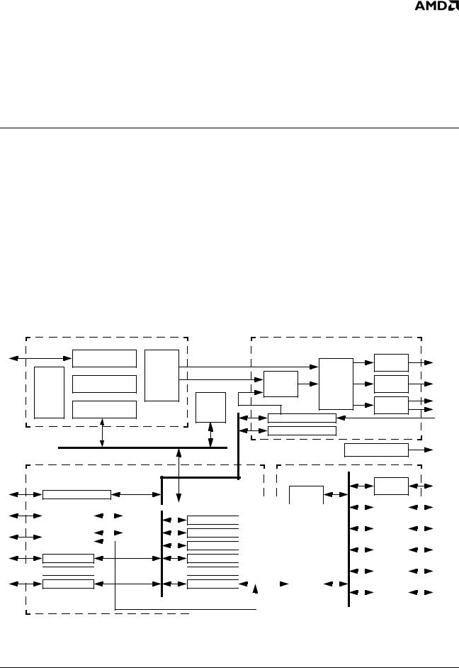
Figure 1-1 shows the relationships between the modules.
GX1 |
|
|
Video Processor |
|
|
|
|
Memory Controller |
|
|
|
CRT I/F |
|
|
|
|
|
|
|
|
|
|
Display |
|
|
|
|
|
2D Graphics |
Controller |
Video |
Video |
TFT I/F |
|
CPU |
Accelerator |
|
Scaling |
Mixer |
|
|
|
|
|
||||
Core |
|
|
Config. |
|
|
|
|
PCI Bus |
|
|
TV I/F |
VOP |
|
|
|
Block |
|
|||
|
Controller |
|
|
|
||
|
|
|
|
|
||
|
|
Video Input Port (VIP) |
|
|
||
|
|
|
|
|
||
|
|
|
Host Interface |
|
|
|
|
|
Fast-PCI Bus |
|
|
|
|
|
|
|
|
|
Clock & Reset Logic |
|
|
|
|
Fast X-Bus |
|
|
|
|
|
|
|
|
Parallel |
|
|
IDE I/F |
|
Core Logic |
RTC |
Port |
|
|
|
|
|
|||
|
|
|
|
|
|
Bridge |
|
|
|
|
|
|
|
|
|
||
USB |
|
|
|
|
PCI Bus |
|
|
|
|
|
|
|
|
|
|||
|
|
|
|
|
|
|
||
PCI/Sub-ISA |
|
|
||||||
|
|
|
||||||
Bus I/F |
|
|
|
|
|
|
|
|
|
|
|
|
|
|
|
|
|
GPIO


 Audio Codec I/F


LPC I/F
X-Bus
|
|
|
|
|
|
|
|
|
|
|
|
|
|
|
|
|
|
|
|
|
|
|
|
|
|
|
|
|
|
|
|
|
|
|
|
ACB1 |
|
|
|
|||||
|
|
|
|
|
|
|
|
|
|
|
|
|
|
|
|
|
|
|
|
|
|
|
|
|
|
|
|
|
|
|
|
|
|
|
|
|
|
|
|
|||||
|
|
|
|
|
|
|
|
|
|
|
|
|
|
|
|
|
|
|
|
|
|
|
|
|
|
|
|
|
|
|
|
|
|
|
|
|
I/F |
|
|
|
||||
|
|
PIT |
|
|
|
|
|
|
|
|
|
|
|
|
|
|
|
|
|
|
|
|
|
|
|
|
|
|
|
|
|
|
|
|
|
|
|
|
|
|
||||
|
|
|
|
|
|
|
|
|
|
|
|
|
|
|
SuperI/O |
|
|
|
|
|
|
ACB2 |
|
|
||||||||||||||||||||
|
|
PIC |
|
|
|
|
|
|
|
|
|
|
|
|
I/F |
|
|
|
|
|||||||||||||||||||||||||
|
DMAC |
|
|
|
|
|
|
|
|
|
|
|
|
|
|
|
|
|
|
|
|
|
|
|
|
|
|
|
|
|
|
|
|
|
|
|
|
|
|
|||||
|
|
|
|
|
|
|
|
|
|
|
|
|
|
|
|
|
|
|
|
|
|
|
|
|
|
|
|
|
|
UART1 |
|
|
|
|
||||||||||
|
|
|
|
|
|
|
|
|
|
|
|
|
|
|
|
|
|
|
|
|
|
|
|
|
|
|
|
|
|
|
|
|
|
|
|
|
|
|
|
|||||
Pwr Mgmnt |
|
|
|
|
|
|
|
|
|
|
|
|
|
|
|
|
|
|
|
|
|
|
|
|
|
|
|
|
|
|
|
|
|
|
|
|
||||||||
|
|
|
|
|
|
|
|
|
|
|
|
|
|
|
|
|
|
|
|
|
|
|
|
|
|
|
|
|
|
|
|
|
|
|
|
|
|
|||||||
|
|
|
|
|
|
|
|
|
|
|
|
|
|
|
|
|
|
|
|
|
|
|
|
|
|
|
|
|
|
|
|
|
|
|
|
|||||||||
Configuration |
|
|
|
|
|
|
|
|
|
|
|
|
|
|
|
|
|
|
|
|
|
|
|
|
|
|
|
UART2 |
|
|
||||||||||||||
|
|
|
|
|
|
|
|
|
|
|
|
|
|
|
|
|
|
|
|
|
|
|
|
|
|
|
|
|
|
|
|
|
||||||||||||
ISA Bus I/F |
|
|
|
|
|
|
|
|
|
|
ISA Bus |
|
|
|
|
|
|
|
|
|
|
|
|
|
|
|
|
|
|
|
|
|
|
|
||||||||||
|
|
|
|
|
|
|
|
|
|
|
I/F |
|
|
|
|
|
|
|
|
|
|
|
|
|
|
UART3 |
|
|
|
|
||||||||||||||
|
|
|
|
|
|
|
|
|
|
|
|
|
|
|
|
|
|
|
|
|
|
|
|
|
|
|
|
|
|
|
|
|
|
|
||||||||||
|
|
|
|
|
|
|
|
|
|
|
|
|
|
|
|
|
|
|
|
|
|
|
|
|
|
|
|
|
|
|
|
|
|
|
|
& IR |
|
|
||||||
|
|
|
|
|
|
|
|
|
|
|
|
|
|
|
|
|
|
|
|
|
|
|
|
|
|
|
|
|
|
|
|
|
|
|
|
|
||||||||
|
|
|
|
|
|
|
|
|
|
|
|
|
|
|
|
|
|
|
|
|
|
|
|
|
|
|
|
|
|
|
|
|
|
|
|
|
|
|
|
|
|
|
|
|
Figure 1-1. Block Diagram
AMD Geode™ SC1200/SC1201 Processor Data Book |
13 |

32579B |
Overview |
1.2Features
General Features
■32-Bit x86 processor, up to 266 MHz, with MMX instruction set support
■Memory controller with 64-bit SDRAM interface
■2D graphics accelerator
■CRT controller with hardware video accelerator
■CCIR-656 video input port with direct video for full screen display
■PC/AT functionality
■PCI bus controller
■IDE interface, two channels
■USB, three ports, OHCI (OpenHost Controller Interface) version 1.0 compliant
■Audio, AC97/AMC97 version 2.0 compliant
■Virtual System Architecture™ technology (VSA) support
■Power management, ACPI (Advanced Configuration Power Interface) version 1.0 compliant
■Package:
— BGU481 (481-Terminal Ball Grid Array Cavity Up)
GX1 Processor Module
■CPU Core:
—32-Bit x86, 266 MHz, with MMX compatible instruction set support
—16 KB unified L1 cache
—Integrated FPU (Floating Point Unit)
—Re-entrant SMM (System Management Mode) enhanced for VSA
■2D Graphics Accelerator:
—Accelerates BitBLTs, line draw and text
—Supports all 256 raster operations
—Supports transparent BLTs
—Runs at core clock frequency
■Memory Controller:
—64-Bit SDRAM interface
—66 to 100 MHz frequency range
—Direct interface with CPU/cache, display controller and 2D graphic accelerator
—Supports clock suspend and power-down/ self-refresh
—Up to two banks of SDRAM (8 devices total) or one SODIMM
■Display Controller:
—Hardware graphics frame buffer compress/ decompress
—Hardware cursor, 32x32 pixels
Video Processor Module
■Video Accelerator:
—Flexible video scaling support of up to 8x (horizontally and vertically)
—Bilinear interpolation filters (with two taps, and eight phases) to smooth output video
■Video/Graphics Mixer:
—8-Bit value alpha blending
—Three blending windows with constant alpha value
—Color key
■Video Input Port (VIP):
—Video capture or display
—CCIR-656 and VESA Video Interface Port v1.1 compliant
—Lock display timing to video input timing (GenLock)
—Able to transfer video data into main memory
—Direct video transfer for full screen display
—Separate memory location for VBI
■Video Output Port (VOP):
—VESA Video Interface Port Rev. 1.1 Task B format
■CRT Interface:
—Uses three 8-bit DACs
—Support up to 135 MHz
—1280x1024 non-interlaced CRT @ 8 bpp, up to 75 Hz
—1024x768 non-interlaced CRT @ 16 bpp, up to 85 Hz
■TFT Interface:
—Direct connection to TFT panels
—800x600 non-interlaced TFT @ 16 bpp graphics, up to 85 Hz
—1024x768 non-interlaced TFT @ 16 bpp graphics, up to 75 Hz
—TFT on IDE: FPCLK max is 40 MHz
—TFT on Parallel Port: FPCLK max is 80 MHz
■TV Interface:
—Uses four 10-bit DACs
—720x480 NTSC @ 60 Hz or 720x576 PAL @ 50 Hz
—NTSC-M, PAL-M/B/D/G/H/I
—Luminance filtering with 2x oversampling and sinx/x correction
—Chrominance filtering with 4x oversampling
—Flicker filter with a three-line buffer for graphics display on TV
—Composite, S-Video and YCrCb component video outputs
—Analog video output interface supports SCART standard (both RGBCvbs and YCCvbs)
—Support for VBI (Vertical Blanking Interval) transfer from Video Port input to TV Encoder
14 |
AMD Geode™ SC1200/SC1201 Processor Data Book |

Overview |
32579B |
—VBI Generation Support:
–Wide Screen Signaling (WSS)
–Closed caption
–Extended Data Services (EDS)
–Copy Generation Management System (CGMS)
—Four-field NTSC or eight-field PAL generation
—Macrovision copy protection version 7.1.L1 (SC1201 only, see "Macrovision Product Notice" on page 441)
Core Logic Module
■Audio Codec Interface:
—AC97/AMC97 (Rev. 2.0) codec interface
—Six DMA channels
■PC/AT Functionality:
—Programmable Interrupt Controller (PIC), 8259Aequivalent
—Programmable Interval Timer (PIT), 8254-equivalent
—DMA Controller (DMAC), 8237-equivalent
■Power Management:
—ACPI v1.0 compliant
—Sx state control of three power planes
—Cx/Sx state control of clocks and PLLs
—Thermal event input
—Wakeup event support:
–Three general-purpose events
–AC97 codec event
–UART2 RI# signal
–Infrared (IR) event
■General Purpose I/Os (GPIOs):
—27 multiplexed GPIO signals
■Low Pin Count (LPC) Bus Interface:
—Specification v1.0 compatible
■PCI Bus Interface:
—PCI v2.1 compliant with wakeup capability
—32-Bit data path, up to 33 MHz
—Glueless interface for an external PCI device
—Fixed priority
—3.3V signal support only
■Sub-ISA Bus Interface:
—Up to 16 MB addressing
—Supports a chip select for ROM or Flash EPROM boot device
—Supports either:
–M-Systems DiskOnChip DOC2000 Flash file system
–NAND EEPROM
—Supports up to two chip selects for external I/O devices
—8-Bit (optional 16-bit) data bus width
—Shares balls with PCI signals
—Is not a subtractive agent
■IDE Interface:
—Two IDE channels for up to four external IDE devices
—Supports ATA-33 synchronous DMA mode transfers, up to 33 MB/s
■Universal Serial Bus (USB):
—USB OpenHCI 1.0 compliant
—Three ports
SuperI/O Module
■Real-Time Clock (RTC):
—DS1287, MC146818 and PC87911 compatible
—Multi-century calendar
■ACCESS.bus (ACB) Interface:
—Two ACB interface ports
■Parallel Port:
—EPP 1.9 compliant
—IEEE 1284 ECP compliant, including level 2
■Serial Port (UART):
—UART1, 16550A compatible (SIN, SOUT, BOUT pins), used for SmartCard interface
—UART2, 16550A compatible
—Enhanced UART with fast Infrared (IR)
Other Features
■High-Resolution Timer:
—32-Bit counter with 1 µs count interval
■WATCHDOG Timer:
—Interfaces to INTR, SMI, Reset
■Clocks:
—Input (external crystals):
–32.768 KHz (internal clock oscillator)
–27 MHz (internal clock oscillator)
—Output:
–AC97 clock (24.576 MHz)
–Memory controller clock (66 MHz to 100 MHz)
–PCI clock (33 MHz)
■JTAG Testability:
—Bypass, Extest, Sample/Preload, IDcode, Clamp, HiZ
■Voltages:
—Internal logic: 266 MHz @ 1.8V
—Standby logic: 266 MHz @ 1.8V
—I/O: 3.3V
—Standby I/O: 3.3V
—Battery (if used): 3.0V
AMD Geode™ SC1200/SC1201 Processor Data Book |
15 |

32579B |
Overview |
|
|
16 |
AMD Geode™ SC1200/SC1201 Processor Data Book |

Architecture Overview |
32579B |
|
|
Architecture Overview2
As illustrated in Figure 1-1 on page 13, the SC1200/ SC1201 processor contains the following modules in one integrated device:
•GX1 Module:
—Combines advanced CPU performance with MMX support, fully accelerated 2D graphics, a 64-bit synchronous DRAM (SDRAM) interface and a PCI bus controller. Integrates GX1 silicon revision 8.1.1.
•Video Processor Module:
—A low-power CRT and TFT support module with a hardware video accelerator for scaling, filtering and color space conversion, and a video input port (VIP). Includes an NTSC/PAL TV encoder.
•Core Logic Module:
—Includes PC/AT functionality, an IDE interface, a Universal Serial Bus (USB) interface, ACPI 1.0 compliant power management, and an audio codec interface.
•SuperI/O Module:
—Includes two Serial Ports, an Infrared (IR) Port, a Parallel Port, two ACCESS.bus interfaces, and a Real-Time Clock (RTC).
2.1GX1 Module
The GX1 processor (silicon revision 8.1.1) is the central module of the SC1200/SC1201 processor. For detailed information regarding the GX1 module, refer to the AMD Geode™ GX1 Processor Data Book and the AMD Geode™ GX1 Processor Silicon Revision 8.1.1 Specification Update documents.
The SC1200/SC1201 processor’s device ID is contained in the GX1 module. Software can detect the revision by reading the DIR0 and DIR1 Configuration registers (see Configuration registers in the AMD Geode™ GX1 Processor Data Book). The AMD Geode™ SC1200/SC1201 Processor Specification Update document contains the specific values.
2.1.1Memory Controller
The GX1 module is connected to external SDRAM devices. For more information see Section 3.4.2 "Memory Interface Signals" on page 50, and the “Memory Controller” chapter in the AMD Geode™ GX1 Processor Data Book.
There are some differences in the SC1200/SC1201 processor’s memory controller and the stand-alone GX1 processor’s memory controller:
1)There is drive strength/slew control in the SC1200/ SC1201 that is not in the GX1. The bits that control this function are in the MC_MEM_CNTRL1 and MC_MEM_CNTRL2 registers. In the GX1 processor, these bits are marked as reserved.
2)The SC1200/SC1201 supports two banks of memory. The GX1 supports four banks of memory. In addition, the SC1200/SC1201 supports a maximum of eight devices and the GX1 supports up to 32 devices. With this difference, the MC_BANK_CFG register is different.
Table 2-1 on page 18 summarizes the 32-bit registers contained in the SC1200/SC1201 processor’s memory controller. Table 2-2 on page 18 gives detailed register/bit formats.
AMD Geode™ SC1200/SC1201 Processor Data Book |
17 |

32579B Architecture Overview
Table 2-1. SC1200/SC1201 Processor Memory Controller Register Summary
GX_BASE+ |
Width |
|
|
|
Memory Offset |
(Bits) |
Type |
Name/Function |
Reset Value |
|
|
|
|
|
8400h-8403h |
32 |
R/W |
MC_MEM_CNTRL1. Memory Controller Control Register 1 |
248C0040h |
|
|
|
|
|
8404h-8407h |
32 |
R/W |
MC_MEM_CNTRL2. Memory Controller Control Register 2 |
00000801h |
|
|
|
|
|
8408h-840Bh |
32 |
R/W |
MC_BANK_CFG. Memory Controller Bank Configuration |
41104110h |
|
|
|
|
|
840Ch-840Fh |
32 |
R/W |
MC_SYNC_TIM1. Memory Controller Synchronous Timing |
2A733225h |
|
|
|
Register 1 |
|
|
|
|
|
|
8414h-8417h |
32 |
R/W |
MC_GBASE_ADD. Memory Controller Graphics Base |
00000000h |
|
|
|
Address Register |
|
|
|
|
|
|
8418h-841Bh |
32 |
R/W |
MC_DR_ADD. Memory Controller Dirty RAM Address |
00000000h |
|
|
|
Register |
|
|
|
|
|
|
841Ch-841Fh |
32 |
R/W |
MC_DR_ACC. Memory Controller Dirty RAM Access |
0000000xh |
|
|
|
Register |
|
|
|
|
|
|
Table 2-2. SC1200/SC1201 Processor Memory Controller Registers
Bit |
Description |
|
|
|
|
|
|
GX_BASE+ 8400h-8403h |
MC_MEM_CNTRL1 (R/W) |
Reset Value: 248C0040h |
|
|
|
|
|
31:30 |
MDCTL (MD[63:0] Drive Strength). 11 is strongest, 00 is weakest. |
|
|
|
|
|
|
29 |
RSVD (Reserved). Write as 0. |
|
|
|
|
|
|
28:27 |
MABACTL (MA[12:0] and BA[1:0] Drive Strength). 11 is strongest, 00 is weakest. |
|
|
|
|
|
|
26 |
RSVD (Reserved). Write as 0. |
|
|
|
|
||
25:24 |
MEMCTL (RASA#, CASA#, WEA#, CS[1:0]#, CKEA, DQM[7:0] Drive Strength). 11 is strongest, 00 is weakest. |
||
|
|
|
|
23:22 |
RSVD (Reserved). Write as 0. |
|
|
|
|
||
21 |
RSVD (Reserved). Must be written as 0. Wait state on the X-Bus x_data during read cycles - for debug only. |
||
|
|
|
|
20:18 |
SDCLKRATE (SDRAM Clock Ratio). Selects SDRAM clock ratio. |
|
|
|
000: Reserved |
100: ÷ 3.5 |
|
|
001: ÷ 2 |
101: ÷ 4 |
|
|
010: ÷ 2.5 |
110: ÷ 4.5 |
|
|
011: ÷ 3 (Default) |
111: ÷ 5 |
|
|
Ratio does not take effect until the SDCLKSTRT bit (bit 17 of this register) transitions from 0 to 1. |
||
|
|
||
17 |
SDCLKSTRT (Start SDCLK). Start operating SDCLK using the new ratio and shift value (selected in bits [20:18] of this reg- |
||
|
ister). |
|
|
|
0: Clear. |
|
|
|
1: Enable. |
|
|
|
This bit must transition from zero (written to zero) to one (written to one) in order to start SDCLK or to change the shift value. |
||
|
|
||
16:8 |
RFSHRATE (Refresh Interval). This field determines the number of processor core clocks multiplied by 64 between refresh |
||
|
cycles to the DRAM. By default, the refresh interval is 00h. Refresh is turned off by default. |
|
|
|
|
||
7:6 |
RFSHSTAG (Refresh Staggering). This field determines number of clocks between the RFSH commands to each of the |
||
|
four banks during refresh cycles: |
|
|
|
00: 0 SDRAM clocks |
|
|
|
01: 1 SDRAM clocks (Default) |
|
|
|
10: 2 SDRAM clocks |
|
|
|
11: 4 SDRAM clocks |
|
|
|
Staggering is used to help reduce power spikes during refresh by refreshing one bank at a time. If only one bank is installed, |
||
|
this field must be written as 00. |
|
|
|
|
||
5 |
2CLKADDR (Two Clock Address Setup). Assert memory address for one extra clock before CS# is asserted. |
||
|
0: Disable. |
|
|
|
1: Enable. |
|
|
|
This can be used to compensate for address setup at high frequencies and/or high loads. |
|
|
|
|
|
|
|
|
|
|
18 |
|
AMD Geode™ SC1200/SC1201 Processor Data Book |
|

Architecture Overview |
32579B |
Table 2-2. SC1200/SC1201 Processor Memory Controller Registers (Continued)
Bit Description
4 RFSHTST (Test Refresh). This bit, when set high, generates a refresh request. This bit is only used for testing purposes.
3XBUSARB (X-Bus Round Robin). When round robin is enabled, processor, graphics pipeline, and low priority display controller requests are arbitrated at the same priority level. When disabled, processor requests are arbitrated at a higher priority level. High priority display controller requests always have the highest arbitration priority.
0:Disable.
1:Enable round robin.
2SMM_MAP (SMM Region Mapping). Maps the SMM memory region at GX_BASE+400000 to physical address A0000 to BFFFF in SDRAM.
0:Disable.
1:Enable.
1 RSVD (Reserved). Write as 0.
0SDRAMPRG (Program SDRAM). When this bit is set, the memory controller will program the SDRAM MRS register using LTMODE in MC_SYNC_TIM1.
This bit must transition from zero (written to zero) to one (written to one) in order to program the SDRAM devices.
GX_BASE+8404h-8407h |
MC_MEM_CNTRL2 (R/W) |
Reset Value: 00000801h |
|
|
|
|
|
31:14 |
RSVD (Reserved). Write as 0. |
|
|
|
|
||
13:12 |
SDCLKCTL (SDCLK High Drive/Slew Control). Controls the high drive and slew rate of SDCLK[3:0] and SDCLK_OUT. |
||
|
11 is strongest, 00 is weakest. |
|
|
|
|
|
|
11 |
RSVD (Reserved). Write as 0. |
|
|
10SDCLKOMSK# (Enable SDCLK_OUT). Turns on the output.
0:Enable.
1:Disable.
9SDCLK3MSK# (Enable SDCLK3). Turns on the output.
0:Enable.
1:Disable.
8SDCLK2MSK# (Enable SDCLK2). Turns on the output.
0:Enable.
1:Disable.
7SDCLK1MSK# (Enable SDCLK1). Turns on the output.
0:Enable.
1:Disable.
6SDCLK0MSK# (Enable SDCLK0). Turns on the output.
0:Enable.
1:Disable.
5:3 SHFTSDCLK (Shift SDCLK). This function allows shifting SDCLK to meet SDRAM setup and hold time requirements. The shift function will not take effect until the SDCLKSTRT bit (bit 17 of MC_MEM_CNTRL1) transitions from 0 to 1:
000: No shift |
100: Shift 2 core clocks |
001: Shift 0.5 core clock |
101: Shift 2.5 core clocks |
010: Shift 1 core clock |
110: Shift 3 core clocks |
011: Shift 1.5 core clock |
111: Reserved |
2 RSVD (Reserved). Write as 0.
1 RD (Read Data Phase). Selects if read data is latched one or two core clock after the rising edge of SDCLK.
0:1 Core clock.
1:2 Core clocks.
0FSTRDMSK (Fast Read Mask). Do not allow core reads to bypass the request FIFO.
0:Disable.
1:Enable.
AMD Geode™ SC1200/SC1201 Processor Data Book |
19 |

32579B Architecture Overview
Table 2-2. SC1200/SC1201 Processor Memory Controller Registers (Continued)
Bit |
Description |
|
|
|
|
|
|
|
|
|
|
GX_BASE+8408h-840Bh |
|
MC_BANK_CFG (R/W) |
Reset Value: 41104110h |
||
|
|
|
|
|
|
31:16 |
RSVD (Reserved). Write as 0070h |
|
|
|
|
|
|
|
|
|
|
15 |
RSVD (Reserved). Write as 0. |
|
|
|
|
|
|
||||
14 |
SODIMM_MOD_BNK (SODIMM Module Banks - Banks 0 and 1). Selects number of module banks installed per SODIMM |
||||
|
for SODIMM: |
|
|
|
|
|
0: 1 Module bank (Bank 0 only) |
|
|
|
|
|
1: 2 Module banks (Bank 0 and 1) |
|
|
|
|
|
|
|
|
|
|
13 |
RSVD (Reserved). Write as 0. |
|
|
|
|
|
|
||||
12 |
SODIMM_COMP_BNK (SODIMM Component Banks - Banks 0 and 1). Selects the number of component banks per |
||||
|
module bank for SODIMM: |
|
|
|
|
|
0: 2 Component banks |
|
|
|
|
|
1: 4 Component banks |
|
|
|
|
|
Banks 0 and 1 must have the same number of component banks. |
|
|||
|
|
|
|
|
|
11 |
RSVD (Reserved). Write as 0. |
|
|
|
|
|
|
|
|||
10:8 |
SODIMM_SZ (SODIMM Size - Banks 0 and 1). Selects the size of SODIMM: |
|
|||
|
000: 4 MB |
010: 16 MB |
100: 64 MB |
110: 256 MB |
|
|
001: 8 MB |
011: 32 MB |
101: 128 MB |
111: 512 MB |
|
|
This size is the total of both banks 0 and 1. Also, banks 0 and 1 must be the same size. |
|
|||
|
|
|
|
|
|
7 |
RSVD (Reserved). Write as 0. |
|
|
|
|
|
|
|
|||
6:4 |
SODIMM_PG_SZ (SODIMM Page Size - Banks 0 and 1). Selects the page size of SODIMM: |
|
|||
|
000: 1 KB |
010: 4 KB |
1xx: 16 KB |
|
|
|
001: 2 KB |
011: 8 KB |
111: SODIMM not installed |
|
|
|
Both banks 0 and 1 must have the same page size. |
|
|
||
|
|
|
|
|
|
3:0 |
RSVD (Reserved). Write as 0. |
|
|
|
|
|
|
|
|
|
|
GX_BASE+840Ch-840Fh |
|
MC_SYNC_TIM1 (R/W) |
Reset Value: 2A733225h |
||
|
|
|
|
|
|
31 |
RSVD (Reserved). Write as 0. |
|
|
|
|
|
|
||||
30:28 |
LTMODE (CAS Latency). CAS latency is the delay, in SDRAM clock cycles, between the registration of a read command |
||||
|
and the availability of the first piece of output data. This parameter significantly affects system performance. Optimal setting |
||||
|
should be used. If an SODIMM is used, BIOS can interrogate EEPROM across the ACCESS.bus interface to determine this |
||||
|
value: |
|
|
|
|
|
000: Reserved |
010: 2 CLK |
100: 4 CLK |
110: 6 CLK |
|
|
001: Reserved |
011: 3 CLK |
101: 5 CLK |
111: 7 CLK |
|
|
This field will not take effect until SDRAMPRG (bit 0 of MC_MEM_CNTRL1) transitions from 0 to 1. |
||||
|
|
||||
27:24 |
RC (RFSH to RFSH/ACT Command Period, tRC). Minimum number of SDRAM clock between RFSH and RFSH/ACT |
||||
|
commands: |
|
|
|
|
|
0000: Reserved |
0100: 5 CLK |
1000: 9 CLK |
1100: 13 CLK |
|
|
0001: 2 CLK |
0101: 6 CLK |
1001: 10 CLK |
1101: 14 CLK |
|
|
0010: 3 CLK |
0110: 7 CLK |
1010: 11 CLK |
1110: 15 CLK |
|
|
0011: 4 CLK |
0111: 8 CLK |
1011: 12 CLK |
1111: 16 CLK |
|
|
|
||||
23:20 |
RAS (ACT to PRE Command Period, tRAS). Minimum number of SDRAM clocks between ACT and PRE commands: |
||||
|
0000: Reserved |
0100: 5 CLK |
1000: 9 CLK |
1100: 13 CLK |
|
|
0001: 2 CLK |
0101: 6 CLK |
1001: 10 CLK |
1101: 14 CLK |
|
|
0010: 3 CLK |
0110: 7 CLK |
1010: 11 CLK |
1110: 15 CLK |
|
|
0011: 4 CLK |
0111: 8 CLK |
1011: 12 CLK |
1111: 16 CLK |
|
|
|
|
|
|
|
19 |
RSVD (Reserved). Write as 0. |
|
|
|
|
|
|
||||
18:16 |
RP (PRE to ACT Command Period, tRP). Minimum number of SDRAM clocks between PRE and ACT commands: |
||||
|
000: Reserved |
010: 2 CLK |
100: 4 CLK |
110: 6 CLK |
|
|
001: 1 CLK |
011: 3 CLK |
101: 5 CLK |
111: 7 CLK |
|
|
|
|
|
|
|
15 |
RSVD (Reserved). Write as 0. |
|
|
|
|
|
|
||||
14:12 |
RCD (Delay Time ACT to READ/WRT Command, tRCD). Minimum number of SDRAM clock between ACT and READ/ |
||||
|
WRT commands. This parameter significantly affects system performance. Optimal setting should be used: |
||||
|
000: Reserved |
010: 2 CLK |
100: 4 CLK |
110: 6 CLK |
|
|
001: 1 CLK |
011: 3 CLK |
101: 5 CLK |
111: 7 CLK |
|
|
|
|
|
|
|
|
|
|
|
|
|
20 |
|
|
|
AMD Geode™ SC1200/SC1201 Processor Data Book |
|
Architecture Overview |
32579B |
Table 2-2. SC1200/SC1201 Processor Memory Controller Registers (Continued)
Bit Description
11 RSVD (Reserved). Write as 0.
10:8 RRD (ACT(0) to ACT(1) Command Period, tRRD). Minimum number of SDRAM clocks between ACT and ACT command to two different component banks within the same module bank. The memory controller does not perform back-to-back Activate commands to two different component banks without a READ or WRITE command between them. Hence, this field should be written as 001.
7 RSVD (Reserved). Write as 0.
6:4 DPL (Data-in to PRE Command Period, tDPL). Minimum number of SDRAM clocks from the time the last write datum is sampled till the bank is precharged:
000: |
Reserved |
010: 2 CLK |
100: 4 CLK |
110: 6 CLK |
001: |
1 CLK |
011: 3 CLK |
101: 5 CLK |
111: 7 CLK |
3:0 RSVD (Reserved). Leave unchanged. Always returns a 101h.
Note: Refer to the SDRAM manufacturer’s specification for more information on component banks.
GX_BASE+8414h-8417h |
MC_GBASE_ADD (R/W) |
Reset Value: 00000000h |
31:18 RSVD (Reserved). Write as 0.
17TE (Test Enable TEST[3:0]).
0:TEST[3:0] are driven low (normal operation).
1:TEST[3:0] pins are used to output test information
16TECTL (Test Enable Shared Control Pins).
0:RASB#, CASB#, CKEB, WEB# (normal operation).
1:RASB#, CASB#, CKEB, WEB# are used to output test information
15:12 SEL (Select). This field is used for debug purposes only and should be left at zero for normal operation.
11 RSVD (Reserved). Write as 0.
10:0 GBADD (Graphics Base Address). This field indicates the graphics memory base address, which is programmable on 512 KB boundaries. This field corresponds to address bits [29:19].
Note that BC_DRAM_TOP must be set to a value lower than the Graphics Base Address.
GX_BASE+8418h-841Bh |
MC_DR_ADD (R/W) |
Reset Value: 00000000h |
31:10 RSVD (Reserved). Write as 0.
9:0 DRADD (Dirty RAM Address). This field is the address index that is used to access the Dirty RAM with the MC_DR_ACC register. This field does not auto increment.
GX_BASE+841Ch-841Fh |
MC_DR_ACC (R/W) |
Reset Value: 0000000xh |
31:2 RSVD (Reserved). Write as 0.
1 D (Dirty Bit). This bit is read/write accessible.
0 V (Valid Bit). This bit is read/write accessible.
AMD Geode™ SC1200/SC1201 Processor Data Book |
21 |

32579B |
Architecture Overview |
2.1.2Fast-PCI Bus
The GX1 module communicates with the Core Logic module via a Fast-PCI bus that can work at up to 66 MHz. The Fast-PCI bus is internal for the SC1200/SC1201 processor and is connected to the General Configuration Block (see Section 4.0 on page 71 for details on the General Configuration Block).
This bus supports seven bus masters. The requests (REQs) are fixed in priority. The seven bus masters in order of priority are:
1)VIP
2)IDE Channel 0
3)IDE Channel 1
4)Audio
5)USB
6)External REQ0#
7)External REQ1#
2.1.3Display
The GX1 module generates display timing, and controls internal signals CRT_VSYNC and CRT_HSYNC of the Video Processor module.
The GX1 module interfaces with the Video Processor via a video data bus and a graphics data bus.
•Video data. The GX1 module uses the core clock, divided by 2 or 4 (typically 100 to 133 MHz). It drives the video data using this clock. Internal signals VID_VAL and VID_RDY are used as data-flow handshake signals between the GX1 module and the Video Processor.
•Graphics data. The GX1 module uses the internal DCLK signal, supplied by the PLL of the Video Processor, to drive the 18-bit graphics-data bus of the Video Processor. Each six bits of this bus define a different color. Each of these 6-bit color definitions is expanded (by adding two zero LSB lines) to form an 8-bit bus, at the Video Processor.
For more information about the GX1 module’s interface to the Video Processor, see the “Display Controller” chapter in the AMD Geode™ GX1 Processor Data Book.
2.2Video Processor Module
The Video Processor provides high resolution and graphics for a CRT, TV, or TFT/DSTN interface. The following subsections provide a summary of how the Video Processor interfaces with the other modules of the SC1200/SC1201 processor. For detailed information about the Video Processor, see Section 7.0 on page 311.
2.2.1GX1 Module Interface
The Video Processor is connected to the GX1 module in the following way:
•The Video Processor’s DOTCLK output signal is used as the GX1 module’s DCLK input signal.
•The GX1 module’s PCLK output signal is used as the GFXCLK input signal of the Video Processor.
2.2.2Video Input Port
The Video Input Port (VIP) within the Video Processor contains a standard interface that is typically connected to a media processor or TV encoder. The clock is supplied by the externally connected device; typically at 27 MHz.
Video input can be sent to the GX1 module’s video frame buffer (Capture Video mode) or can be used directly (Direct Video mode).
2.2.3Core Logic Module Interface
The Video Processor interfaces to the Core Logic module for accessing PCI function configuration registers.
2.2.4CRT DAC
The Video Processor drives three CRT DACs with up to 135M pixels per second.
The interface for these DACs can be monitored via external balls of the SC1200/SC1201 processor. For more information, see Section 3.4.4 "CRT/TFT Interface Signals" on page 52.
2.3Core Logic Module
The Core Logic module is described in detail in Section 6.0 on page 141.
The Core Logic module is connected to the Fast-PCI bus. It uses signal AD28 as the IDSEL for all PCI configuration functions except for USB which uses AD29.
2.3.1Other Core Logic Module Interfaces
The following interfaces of the Core Logic module are implemented via external signals of the SC1200/SC1201 processor. Each interface is listed below with a reference to the descriptions of the relevant signals.
•IDE: See Section 3.4.10 "IDE Interface Signals" on page 61.
•AC97: See Section 3.4.15 "AC97 Audio Interface Signals" on page 65.
•PCI: See Section 3.4.7 "PCI Bus Interface Signals" on page 55.
22 |
AMD Geode™ SC1200/SC1201 Processor Data Book |

Architecture Overview |
32579B |
•USB: See Section 6.2.4 "Universal Serial Bus" on page 147. The USB function uses signal AD29 as the IDSEL for PCI configuration.
•LPC: See Section 3.4.9 "Low Pin Count (LPC) Bus Interface Signals" on page 60.
•Sub-ISA: See Section 3.4.8 "Sub-ISA Interface Signals" on page 59, Section 6.2.5 "Sub-ISA Bus Interface" on page 147, and Section 4.2 "Pin Multiplexing, Interrupt Selection, and Base Address Registers" on page 72
•GPIO: See Section 3.4.17 "GPIO Interface Signals" on page 67.
More detailed information about each of these interfaces is provided in Section 6.2 "Module Architecture" on page 142.
•Super/IO Block Interfaces: See Section 4.2 "Pin Multiplexing, Interrupt Selection, and Base Address Registers" on page 72, Section 3.4.6 "ACCESS.bus Interface Signals" on page 55, Section 3.4.14 "Fast Infrared (IR) Port Interface Signals" on page 64, and Section 3.4.13 "Parallel Port Interface Signals" on page 63.
The Core Logic module interface to the GX1 module consists of seven miscellaneous connections, the PCI bus interface signals, plus the display controller connections. Note that the PC/AT legacy signals NMI, WM_RST, and A20M are all virtual functions executed in SMM (System Management Mode) by the BIOS.
•PSERIAL is a one-way serial bus from the GX1 to the Core Logic module used to communicate powermanagement states and VSYNC information for VGA emulation.
•IRQ13 is an input from the processor indicating that a floating point error was detected and that INTR should be asserted.
•INTR is the level output from the integrated 8259A PICs and is asserted if an unmasked interrupt request (IRQn) is sampled active.
•SMI# is a level-sensitive interrupt to the GX1 that can be configured to assert on a number of different system events. After an SMI# assertion, SMM is entered and program execution begins at the base of the SMM address space. Once asserted, SMI# remains active until the SMI source is cleared.
•SUSP# and SUSPA# are handshake signals for implementing CPU Clock Stop and clock throttling.
•CPU_RST resets the CPU and is asserted for approximately 100 µs after the negation of POR#.
•PCI bus interface signals.
2.4SuperI/O Module
The SuperI/O (SIO) module is a PC98 and ACPI compliant SIO that offers a single-cell solution to the most commonly used ISA peripherals.
The SIO module incorporates: two Serial Ports, an Infrared Communication Port that supports FIR, MIR, HP-SIR, Sharp-IR, and Consumer Electronics-IR, a full IEEE 1284 Parallel Port, two ACCESS.bus Interface (ACB) ports, System Wakeup Control (SWC), and a Real-Time Clock (RTC) that provides RTC timekeeping.
2.5Clock, Timers, and Reset Logic
In addition to the four main modules (i.e., GX1, Core Logic, Video Processor and SIO) that make up the SC1200/ SC1201 processor, the following blocks of logic have also been integrated:
•Clock Generators as described in Section 4.5 "Clock Generators and PLLs" on page 83.
•Configuration Registers as described in Section 4.2 "Pin Multiplexing, Interrupt Selection, and Base Address Registers" on page 72.
•A WATCHDOG timer as described in Section 4.3 "WATCHDOG" on page 79.
•A High-Resolution timer as described in Section 4.4 "High-Resolution Timer" on page 81.
2.5.1Reset Logic
This section provides a description of the reset flow of the SC1200/SC1201 processor.
2.5.1.1Power-On Reset
Power-on reset (POR) is triggered by assertion of the POR# signal. Upon power-on reset, the following things happen:
•Strap balls are sampled.
•PLL4, PLL5, and PLL6 are reset, disabling their output. When the POR# signal is negated, the clocks lock and then each PLL outputs its clock. PLL6 is the last clock generator to output a clock. See Section 4.5 "Clock Generators and PLLs" on page 83.
•Certain WATCHDOG and High-Resolution Timer register bits are cleared.
2.5.1.2System Reset
System reset causes signal PCIRST# to be issued, thus triggering a reset of all PCI and LPC agents. A system reset is triggered by any of the following events:
•Power-on, as indicated by POR# signal assertion.
•A WATCHDOG reset event (see Section 4.3.2 "WATCHDOG Registers" on page 80).
•Software initiated system reset.
AMD Geode™ SC1200/SC1201 Processor Data Book |
23 |

32579B |
Architecture Overview |
|
|
24 |
AMD Geode™ SC1200/SC1201 Processor Data Book |
Signal Definitions |
32579B |
|
|
Signal Definitions3
This section defines the signals and describes the external interface of the SC1200/SC1201 processor. Figure 2-1 shows the signals organized by their functional groups. Where signals are multiplexed, the default signal name is
listed first and is separated by a plus sign (+). A slash (/) in a signal name means that the function is always enabled and available (i.e., cycle multiplexed).
|
|
|
|
|
|
|
|
|
|
POR# |
|
|
|
CVBS+Cr+TVB |
|
|
|
|
|
|
|
|
|
|
|
|
|
|
|
|
|
|
|
|
|
|
|
|
|
|
|
||
|
|
|
|
|
|
|
|
|
|
X32I |
|
|
|
SVY+Cb+TVR+CVBS |
|
|
|
|
|
|
|
|
|
|
|
|
|
|
|
|
|
|
|
|
|
|
|
|
|
|
|
||
|
|
|
|
|
|
|
|
|
|
X32O |
|
|
|
SVC+Cr+Cb+TVB+TVR |
|
|
|
|
|
|
TV |
|
|
|
|
|
|
|
|
|
|
|
|
|
|
|
|
|
|
|
|||
System |
|
|
|
|
|
|
|
X27I |
|
|
|
CVBS+Y+TVG |
|
|
|
|
|
|
|||
|
|
|
|
|
|
|
|
|
|
|
|
|
|
|
|||||||
|
|
|
|
|
|
|
X27O |
|
|
|
TVCOMP |
|
|
|
|
|
|
Interface |
|||
|
|
|
|
|
|
|
|
|
|
|
|
|
|
|
|
|
|
|
|
||
Interface |
|
|
|
|
|
|
PCIRST# |
|
|
|
TVRSET |
|
|
|
|
|
|
|
|||
|
|
|
|
|
|
|
|
|
|
|
|
|
|
|
|
||||||
|
|
|
|
|
|
BOOT16+ROMCS# |
|
|
TVREF |
|
|
|
|
|
|
|
|||||
|
|
|
|
|
|
|
|
|
|
|
|
|
|
|
|
|
|
|
|||
|
|
|
|
|
|
|
|
|
|
LPC_ROM+PCICLK1 |
|
|
TVIOM |
|
|
|
|
|
|
|
|
|
|
|
|
|
|
|
|
|
|
|
|
|
|
|
|
|
|
||||
|
|
|
|
|
|
|
|
|
|
TFT_PRSNT+SDATA_OUT |
|
Straps |
|
|
|
|
|
|
|
||
|
|
|
|
|
|
|
|
|
|
|
|
|
|
|
|
|
|||||
|
|
|
|
|
|
|
|
|
|
FPCI_MON+PCICLK0 |
|
|
HSYNC |
|
|
|
|
|
|
|
|
|
|
|
|
|
|
|
|
|
|
|
|
|
|
|
|
|
|
||||
|
|
|
|
|
|
|
|
|
|
DID0+GNT0#, DID1+GNT1# |
|
|
|
|
|
|
|
|
|
||
|
|
|
|
|
|
|
|
|
|
|
|
VSYNC |
|
|
|
|
|
|
CRT |
||
|
|
|
|
|
|
|
|
|
|
|
|
|
|
VREF |
|
|
|
|
|
|
|
|
|
|
|
|
|
|
|
|
|
|
|
|
|
|
|
|
|
|
|
Interface |
|
|
|
|
|
|
|
|
|
|
|
MD[63:0] |
|
|
|
SETRES |
|
|
|
|
|
|
|
|
|
|
|
|
|
|
|
|
|
MA[12:0] |
|
|
|
RED, GREEN, BLUE |
|
|
|
|
|
|
|
|
|
|
|
|
|
|
|
|
|
|
|
|
|
|
|
|
|
|
|
||
|
|
|
|
|
|
|
|
|
|
BA[1:0] |
|
|
|
|
|
|
|
|
|
|
|
|
|
|
|
|
|
|
|
|
|
|
|
|
|
|
|
|
|
|
|
|
|
|
|
|
|
|
|
|
|
|
|
CS[1:0]# |
AMD Geode™ |
IDE_ADDR2+TFTD4 |
|
|
|
|
|
|
|
||
|
|
|
|
|
|
|
|
|
|
|
|
|
|
|
|
|
|||||
|
|
|
|
|
|
|
|
|
|
RASA# |
|
|
|
|
|
|
|
||||
|
|
|
|
|
|
|
|
|
|
IDE_ADDR1+TFTD2 |
|
|
|
|
|
|
|
||||
Memory |
|
|
|
|
|
|
CASA# |
SC1200/SC1201 |
|
|
|
|
|
|
|
||||||
|
|
|
|
|
|
IDE_ADDR0+TFTD3 |
|
|
|
|
|
|
|
||||||||
Interface |
|
|
|
|
|
|
WEA# |
|
|
|
|
|
|
|
|||||||
|
|
|
|
|
|
Processor |
IDE_DATA15+TFTD7 |
|
|
|
|
|
|
|
|||||||
|
|
|
|
|
|
|
|
|
|
DQM[7:0] |
|
|
|
|
|
|
|
||||
|
|
|
|
|
|
|
|
|
|
|
|
|
IDE_DATA14+TFTD17 |
|
|
|
|
|
|
|
|
|
|
|
|
|
|
|
|
|
|
CKEA |
|
|
|
|
|
|
|
|
|
|
|
|
|
|
|
|
|
|
|
|
|
|
|
|
IDE_DATA13+TFTD15 |
|
|
|
|
|
|
|
|
|
|
|
|
|
|
|
|
|
|
SDCLK[3:0] |
|
|
|
|
|
|
|
|
|
|
|
|
|
|
|
|
|
|
|
|
|
|
|
|
IDE_DATA12+TFTD13 |
|
|
|
|
|
|
|
|
|
|
|
|
|
|
|
|
|
|
SDCLK_IN |
|
|
|
|
|
|
|
|
|
|
|
|
|
|
|
|
|
|
|
|
|
|
|
|
IDE_DATA11+GPIO41 |
|
|
|
|
|
|
|
|
|
|
|
|
|
|
|
|
|
|
SDCLK_OUT |
|
|
|
|
|
|
|
|
|
|
|
|
|
|
|
|
|
|
|
|
|
|
|
|
IDE_DATA10+DDC_SCL |
|
|
|
|
|
|
|
|
|
|
|
|
|
|
|
|
|
|
|
|
|
|
|
|
|
|
|
|
|
|
|
|
|
|
|
|
|
|
|
|
|
|
|
|
IDE_DATA9+DDC_SDA |
|
|
|
|
|
|
|
|
|
|
|
|
|
|
|
|
|
|
|
|
|
|
|
|
|
|
|
|
|
ACCESS.bus |
|
|
|
|
|
|
|
|
|
AB1C+GPIO20+DOCCS# |
|
IDE_DATA8+GPIO40 |
|
|
|
|
|
|
|
||
|
|
|
|
|
|
|
|
|
|
|
|
|
|
|
|
|
|||||
|
|
|
|
|
|
|
|
AB1D+GPIO1+IOCS1# |
|
IDE_DATA7+INTD# |
|
|
|
|
|
|
|
||||
|
|
|
|
|
|
|
|
|
|
|
|
|
|
|
|
||||||
Interface |
|
|
|
|
|
|
|
|
GPIO12+AB2C |
|
IDE_DATA6+IRQ9 |
|
|
|
|
|
|
IDE/TFT |
|||
|
|
|
|
|
|
|
|
|
|
|
|
|
|
||||||||
|
|
|
|
|
|
|
|
|
|
GPIO13+AB2D |
|
IDE_DATA5+CLK27M |
|
|
|
|
|
|
|||
|
|
|
|
|
|
|
|
|
|
|
|
|
|
|
|
||||||
|
|
|
|
|
|
|
|
|
|
|
|
|
|
IDE_DATA4+FP_VDD_ON |
|
|
|
|
|
|
Interface |
|
|
|
|
|
|
|
|
|
|
|
|
|
|
|
|
|
|
|
|
||
|
|
|
|
|
|
|
|
|
|
|
|
|
|
IDE_DATA3+TFTD12 |
|
|
|
|
|
|
|
|
|
|
|
|
|
|
|
|
|
ACK#+TFTDE+VOPCK |
|
|
|
|
|
|
|
|
|||
|
|
|
|
|
|
|
|
|
|
|
IDE_DATA2+TFTD14 |
|
|
|
|
|
|
|
|||
|
|
|
|
|
|
|
|
|
|
AFD#/DSTRB#+TFTD2+VOPD1 |
|
|
|
|
|
|
|
|
|||
|
|
|
|
|
|
|
|
|
|
|
IDE_DATA1+TFTD16 |
|
|
|
|
|
|
|
|||
|
|
|
|
|
|
|
|
|
|
BUSY/WAIT#+TFTD3+VOPD2 |
|
|
|
|
|
|
|
|
|||
|
|
|
|
|
|
|
|
|
|
|
IDE_DATA0+TFTD6 |
|
|
|
|
|
|
|
|||
|
|
|
|
|
|
|
|
|
|
ERR#+TFTD4+VOPD3 |
|
|
|
|
|
|
|
|
|||
|
|
|
|
|
|
|
|
|
|
|
IDE_IOR0#+TFTD10 |
|
|
|
|
|
|
|
|||
|
|
|
|
|
|
|
|
|
|
INIT#+TFTD5+VOPD4 |
|
|
|
|
|
|
|
|
|||
Parallel Port/ |
|
|
|
|
|
|
PD7+TFTD13 |
|
|
|
IDE_IOW0#+TFTD9 |
|
|
|
|
|
|
|
|||
|
|
|
|
|
|
|
|
|
IDE_CS0#+TFTD5 |
|
|
|
|
|
|
|
|||||
TFT/VOP Interface |
|
|
|
|
|
|
PD6+TFTD1+VOPD0 |
|
|
|
|
|
|
|
|
||||||
|
|
|
|
|
|
|
IDE_CS1#+TFTDE |
|
|
|
|
|
|
|
|||||||
|
|
|
|
|
|
|
|
|
|
PD[5:0]+TFTD[11:6]+VOPD[7:5] |
|
|
|
|
|
|
|
|
|||
|
|
|
|
|
|
|
|
|
|
PE+TFTD14 |
|
|
|
IDE_IORDY0+TFTD11 |
|
|
|
|
|
|
|
|
|
|
|
|
|
|
|
|
|
|
|
|
IDE_DREQ0+TFTD8 |
|
|
|
|
|
|
|
|
|
|
|
|
|
|
|
|
|
|
SLCT+TFTD15 |
|
|
|
|
|
|
|
|
|||
|
|
|
|
|
|
|
|
|
|
|
IDE_DACK0#+TFTD0 |
|
|
|
|
|
|
|
|||
|
|
|
|
|
|
|
|
|
|
SLIN#/ASTRB#+TFTD16 |
|
|
|
|
|
|
|
|
|||
|
|
|
|
|
|
|
|
|
|
|
IDE_RST#+TFTDCK |
|
|
|
|
|
|
|
|||
|
|
|
|
|
|
|
|
|
|
STB#/WRITE#+TFTD17 |
|
|
|
|
|
|
|
|
|||
|
|
|
|
|
|
|
|
|
|
|
|
|
|
IRQ14+TFTD1 |
|
|
|
|
|
|
|
|
|
|
|
|
|
|
|
|
|
|
|
|
|
|
|
|
|
|
|
|
|
Video Port 

 VPD[7:0]
Interface 

 VPCKIN
Note: Straps are not the default signal, shown with system signals for reader convenience. However, also listed in figure with the appropriate functional group.
Figure 3-1. Signal Groups
AMD Geode™ SC1200/SC1201 Processor Data Book |
25 |
|
32579B |
|
|
Signal Definitions |
|
|
POWER_EN |
PCICLK0+FPCI_MON |
|
||
|
OVER_CUR# |
PCICLK1+LPC_ROM |
|
||
USB |
DPOS_PORT1 |
|
PCICLK |
|
|
DNEG_PORT1 |
|
INTA#, INTB# |
|
||
Interface |
DPOS_PORT2 |
AMD Geode™ |
FRAME# |
|
|
DNEG_PORT2 |
LOCK# |
|
|||
|
SC1200/SC1201 |
|
|||
|
DPOS_PORT3 |
PERR# |
|
||
|
DNEG_PORT3 |
Processor |
SERR# |
|
|
|
|
|
REQ[1:0]# |
|
|
|
SIN1 |
|
GNT0#+DID0 |
|
|
|
|
GNT1#+DID1 |
|
||
|
SIN2+SDTEST3 |
|
|
||
|
|
A[23:0]/AD[23:0] |
|
||
|
SOUT1+CLKSEL1 |
|
|
||
|
|
D[7:0]/AD[31:24] |
|
||
|
SOUT2+CLKSEL2 |
|
|
||
Serial Ports |
|
D[11:8]/C/BE[3:0]# |
Sub-ISA/PCI Bus |
||
GPIO7+RTS2#+IDE_DACK1#+SDTEST0 |
|||||
D12/PAR |
|||||
(UARTs)/IDE |
GPIO8+CTS2#+IDE_DREQ1+SDTEST4 |
Interface |
|||
D13/TRDY# |
|||||
GPIO18+DTR1#/BOUT1 |
|
||||
Interface |
|
D14/IRDY# |
|
||
GPIO6+DTR2#/BOUT2+IDE_IOR1#+SDTEST5 |
|
||||
|
D15/STOP# |
|
|||
|
GPIO11+RI2#+IRQ15 |
|
|
||
|
|
BHE#/DEVSEL# |
|
||
|
|
|
|
||
|
GPIO9+DCD2#+IDE_IOW1#+SDTEST2 GPIO17+TFTDCK+IOCS0# |
|
|||
|
GPIO10+DSR2#+IDE_IORDY1+SDTEST1 |
|
|
||
|
|
GPIO1+IOCS1+TFTD12 |
|
||
IR Port |
|
|
ROMCS#/BOOT16 |
|
|
IRRX1+SIN3 |
GPIO20+DOCCS#+TFTD0 |
|
|||
Interface |
IRTX+SOUT3 |
|
RD#+CLKSEL0 |
|
|
|
|
|
WR# |
|
|
|
BIT_CLK |
GPIO14+DOCR#+IOR# |
|
||
|
GPIO15+DOCW#+IOW# |
|
|||
|
|
|
|||
|
SDATA_OUT+TFT_PRSNT |
GPIO0+TRDE# |
|
||
|
SDATA_IN |
|
|
||
AC97 Audio |
GPIO19+INTC#+IOCHRDY |
|
|||
SDATA_IN2 |
|
||||
|
|
|
|||
Interface |
SYNC+CLKSEL3 |
|
|
|
|
|
AC97_CLK |
|
GPIO32+LAD0 |
|
|
|
AC97_RST# |
|
GPIO33+LAD1 |
|
|
|
GPIO16+PC_BEEP |
|
GPIO34+LAD2 |
GPIO/LPC Bus |
|
|
|
|
GPIO35+LAD3 |
||
|
CLK32 |
|
GPIO36+LDRQ# |
Interface |
|
|
GPIO37+LFRAME# |
|
|||
|
GPWIO[2:0] |
|
|||
Power |
GPIO38+IRRX2+LPCPD |
|
|||
LED# |
|
||||
|
GPIO39+SERIRQ |
|
|||
Management |
ONCTL# |
|
|
||
|
|
|
|||
Interface |
PWRBTN# |
|
TEST1+PLL6B |
|
|
|
PWRCNT[1:2] |
|
|
||
|
THRM# |
|
TEST0+PLL2B |
Test and |
|
|
|
TEST3+GXCLK+FP_VDD_ON |
Measurement |
||
|
|
|
TEST2+PLL5B |
||
|
TCK |
|
Interface |
||
|
|
GTEST |
|||
JTAG |
TDI |
|
|||
|
TDP, TDN |
|
|||
TDO |
|
|
|||
Interface |
|
|
|
||
TMS |
|
|
|
||
|
|
|
|
||
|
TRST# |
|
|
|
|
Figure 3-1. Signal Groups (Continued)
The remaining subsections of this chapter describe:
•Section 3.1 "Ball Assignments": Provides a ball assignment diagram and tables listing the signals sorted according to ball number and alphabetically by signal name.
•Section 3.2 "Strap Options": Several balls are read at power-up that set up the state of the SC1200/SC1201 processor. This section provides details regarding those balls.
•Section 3.3 "Multiplexing Configuration": Lists multiplexing options and their configurations.
•Section 3.4 "Signal Descriptions": Detailed descriptions of each signal according to functional group.
26 |
AMD Geode™ SC1200/SC1201 Processor Data Book |

Signal Definitions |
32579B |
3.1Ball Assignments
The SC1200/SC1201 processor is highly configurable as illustrated in Figure 3-1 on page 25. Strap options and register programming are used to set various modes of operation and specific signals on specific balls. This section describes which signals are available on which balls and provides configuration information:
•Figure 3-2 on page 28: Illustrates the BGU481 ball assignments.
•Table 3-2 on page 29: Lists signals according to ball number. Power Rail, Signal Type, Buffer Type and, where relevant, Pull-Up or Pull-Down resistors are indicated for each ball in this table. For multiplexed balls, the necessary configuration for each signal is listed as well.
•Table 3-3 on page 40: Quick reference signal list sorted alphabetically - listing all signal names and ball numbers.
The tables in this chapter use several common abbreviations. Table 3-1 lists the mnemonics and their meanings
Notes:
1)For each GPIO signal, there is an optional pull-up resistor on the relevant ball. After system reset, the pull-up is present.
This pull-up resistor can be disabled via registers in the Core Logic module. The configuration is without regard to the selected ball function (except for GPIO12, GPIO13, and GPIO16). Alternate functions for GPIO12, GPIO13, and GPIO16 control pull-up resistors.
For more information, see Section 6.4.1 "Bridge, GPIO, and LPC Registers - Function 0" on page 190.
2)Configuration settings listed in this table are with regard to the Pin Multiplexing Register (PMR). See Section 4.2 "Pin Multiplexing, Interrupt Selection, and Base Address Registers" on page 72 for a detailed description of this register.
Table 3-1. Signal Definitions Legend
Mnemonic |
Definition |
|
|
A |
Analog |
|
|
AVSS |
Ground ball: Analog |
|
|
AVCC |
Power ball: Analog |
GCB |
General Configuration Block registers. |
|
Refer to Section 4.0 "General Configura- |
|
tion Block" on page 71. |
|
Location of the General Configuration |
|
Block cannot be determined by software. |
|
See AMD Geode™ SC1200/SC1201 |
|
Processor Specification Update docu- |
|
ment. |
|
|
I |
Input ball |
|
|
I/O |
Bidirectional ball |
|
|
MCR[x] |
Miscellaneous Configuration Register |
|
Bit x: A register, located in the GCB. |
|
Refer to Section 4.1 "Configuration |
|
Block Addresses" on page 71 for further |
|
details. |
|
|
O |
Output ball |
|
|
OD |
Open-drain |
|
|
PD |
Pull-down (KΩ) |
|
|
PMR[x] |
Pin Multiplexing Register Bit x: A regis- |
|
ter, located in the GCB, used to config- |
|
ure balls with multiple functions. Refer to |
|
Section 4.1 "Configuration Block |
|
Addresses" on page 71 for further |
|
details. |
|
|
PU |
Pull-up (KΩ) |
|
|
TS |
TRI-STATE |
|
|
VCORE |
Power ball: 1.2V |
VIO |
Power ball: 3.3V |
VSS |
Ground ball |
# |
The # symbol in a signal name indicates |
|
that the active or asserted state occurs |
|
when the signal is at a low voltage level. |
|
Otherwise, the signal is asserted when |
|
at a high voltage level. |
|
|
/ |
A / in a signal name indicates both func- |
|
tions are always enabled (i.e., cycle mul- |
|
tiplexed). |
|
|
+ |
A + in signal name indicates the function |
|
is available on the ball, but that either |
|
strapping options or register program- |
|
ming is required to select the desired |
|
function. |
|
|
AMD Geode™ SC1200/SC1201 Processor Data Book |
27 |

|
|
|
|
|
|
32579B |
|
|
|
|
|
|
|
|
|
|
|
|
|
|
|
|
|
|
|
Signal Definitions |
|||||||
|
1 |
2 |
3 |
4 |
5 |
6 |
7 |
8 |
9 |
10 |
11 |
12 |
13 |
14 |
15 |
16 |
17 |
18 |
19 |
20 |
21 |
22 |
23 |
24 |
25 |
26 |
27 |
28 |
29 |
30 |
31 |
|
|
A |
|
|
|
S |
|
|
|
|
|
|
|
|
|
|
|
|
|
|
|
|
|
|
|
|
|
|
|
|
|
|
|
A |
|
VSS |
VIO |
AD30 |
PCK0 REQ1# PRST# PCICK |
IOW# |
GP20 |
GP17 |
HSNC |
AVCCCT VSS |
GREEN BLUE |
VSS |
VPLL2 |
PD7 |
VSS |
PD6 |
PD1 |
STB# |
CVBS |
SVY |
TVRST D+P3 |
D-P3 |
D+P1 |
D-P1 |
VIO |
VSS |
|||||||||
|
|
||||||||||||||||||||||||||||||||
B |
|
|
|
|
|
|
|
S |
|
|
|
|
|
|
|
|
|
|
|
|
|
|
|
|
|
|
|
|
|
|
|
B |
|
VSS |
VIO |
AD29 |
AD28 REQ0# AD23 |
VSS |
RD# |
WR# |
VSS |
VSNC |
RED |
VIO |
AVSSCT STRES |
VIO |
BUSY |
ACK# |
VIO |
SLIN# |
INIT# |
VSS |
TVIOM AVSSTV |
VSS |
TVCMP D+P2 |
D-P2 |
GP10 |
VSS |
VIO |
||||||||
|
|
||||||||||||||||||||||||||||||||
C |
|
|
|
|
S |
S |
|
S |
|
|
|
|
|
|
|
|
|
|
|
|
|
|
|
|
|
|
|
|
|
|
|
C |
|
AD26 |
AD24 |
VIO |
AD25 GNT0# GNT1# |
VIO |
RMCS# GP19 |
VIO |
IRTX |
VSSCT |
AVCCCT AVSSCTAVSSCT AVSSP2 SLCT |
PD4 |
PD5 |
PD3 |
PD0 |
VIO |
SVC |
TVREF |
VIO |
INTB# AVSSUSB GP9 |
VIO |
GP7 |
GP8 |
||||||||||||
D |
|
|
|
|
|
S |
|
|
|
|
|
|
|
|
|
|
|
|
|
|
|
|
|
|
|
|
|
|
S |
|
|
D |
|
AD21 |
AD22 |
AD20 |
AD27 |
AD31 |
PCK1 |
VSS |
FRM# |
IOR# |
GP1 |
TRDE# VCCCT |
VSS |
VIO |
AVCCCT VREF |
PE |
VIO |
VSS |
PD2 |
ERR# |
AFD# AVCCTV CVBS |
VSS |
INTA# AVCCUSB GP6 |
SOUT |
TDP |
TDN |
|||||||||
E |
AD16 |
AD19 |
AD18 |
DVSL# |
|
|
|
|
|
|
|
|
|
|
|
|
|
|
|
|
|
|
|
|
|
|
|
SIN2 |
TRST# |
TDO |
TCK |
E |
|
|
|
|
|
|
|
|
|
|
|
|
|
|
|
|
|
|
|
|
|
|
|
|
|
|
|||||||||
F |
TRDY# IRDY# CBE2# |
AD17 |
|
|
|
|
|
|
|
|
|
|
|
|
|
|
|
|
|
|
|
|
|
|
|
TMS |
TDI |
GTST |
VPCKI |
F |
|||
|
|
|
|
|
|
|
|
|
|
|
|
|
|
|
|
|
|
|
|
|
|
|
|
|
|||||||||
G |
STOP# VSS |
VIO |
VSS |
|
|
|
|
|
|
|
|
|
|
|
|
|
|
|
|
|
|
|
|
|
|
|
VSS |
VIO |
VSS |
VPD7 |
G |
||
|
|
|
|
|
|
|
|
|
|
|
|
|
|
|
|
|
|
|
|
|
|
|
|
|
|||||||||
H |
SRR# |
PRR# LOCK# CBE3# |
|
|
|
|
|
|
|
|
|
|
|
|
|
|
|
|
|
|
|
|
|
|
|
VPD6 |
VPD5 |
VPD4 |
VPD3 |
H |
|||
|
|
|
|
|
|
|
|
|
|
|
|
|
|
|
|
|
|
|
|
|
|
|
|
|
|||||||||
J |
AD13 CBE1# |
AD15 |
PAR |
|
|
|
|
|
|
AMD Geode™ |
|
|
|
|
|
VPD2 |
VPD1 |
VPD0 |
GP39 |
J |
|||||||||||||
|
|
|
|
|
|
|
|
|
|
|
|
|
|||||||||||||||||||||
K |
AD11 |
VIO |
VSS |
AD14 |
|
|
|
|
|
|
|
|
|
|
|
GP38 |
VIO |
VSS |
GP37 |
K |
|||||||||||||
L |
|
|
|
|
|
|
|
|
|
|
|
L |
|||||||||||||||||||||
CBE0# |
AD9 |
AD10 |
AD12 |
|
|
|
|
|
|
|
|
|
|
|
|
|
|
|
|||||||||||||||
|
|
|
|
|
|
|
|
|
|
|
|
|
|
|
|
|
|
|
|
|
|
|
GP36 |
GP35 |
GP34 |
GP33 |
|||||||
M |
VSS |
AD7 |
VIO |
AD8 |
|
|
|
|
|
|
|
|
|
|
|
|
|
|
|
|
|
|
|
|
|
|
|
GP32 |
GP13 |
VIO |
VSS |
M |
|
|
|
|
|
|
|
|
|
|
|
|
|
|
|
|
|
|
|
|
|
|
|
|
|
|
|||||||||
N |
AD3 |
AD6 |
AD5 |
VSS |
|
|
|
|
|
|
|
|
VCORE VCORE |
VSS |
VSS |
VSS |
VCORE VCORE |
|
|
|
|
|
|
|
|
VSS |
GP12 |
AB1D |
AB1C |
N |
|||
|
|
|
|
|
|
|
|
|
|
|
|
|
|
|
|
|
|
||||||||||||||||
P |
|
|
|
|
|
|
|
|
|
|
|
|
|
|
|
|
|
|
|
|
|
|
|
|
|
|
|
|
S |
S |
|
P |
|
AD4 |
ICS1# |
AD1 |
VCORE |
|
|
|
|
|
|
|
|
VCORE VCORE |
VSS |
VSS |
VSS |
VCORE VCORE |
|
|
|
|
|
|
|
|
VCORE |
SDO |
SYNC ACCK |
||||||
|
|
|
|
|
|
|
|
|
|
|
|
|
|
|
|
|
|
||||||||||||||||
R |
VSS |
VSS |
VSS |
VSS |
|
|
|
|
|
|
|
|
VSS |
VSS |
VSS |
VSS |
VSS |
VSS |
VSS |
|
|
|
|
|
|
|
|
VSS |
VSS |
VSS |
VSS |
R |
|
|
|
|
|
|
|
|
|
|
|
|
|
|
|
|
|
|
|
||||||||||||||||
T |
VCORE VCORE VCORE VCORE |
|
|
|
|
|
|
|
|
VSS |
VSS |
VSS |
VSS |
VSS |
VSS |
VSS |
|
|
|
|
|
|
|
|
VCORE VCORE VCORE VCORE |
T |
|||||||
|
|
|
|
|
|
|
|
|
|
|
|
|
|
|
|
|
|
||||||||||||||||
U |
AD0 |
IAD2 |
AD2 |
VCORE |
|
|
|
|
|
|
|
|
VSS |
VSS |
VSS |
VSS |
VSS |
VSS |
VSS |
|
|
|
|
|
|
|
|
VCORE ACRST# BITCK SDI |
U |
||||
V |
|
|
|
|
|
|
|
|
|
|
|
|
|
|
|
|
V |
||||||||||||||||
IDAT15 IDAT14 IDAT13 |
VSS |
|
|
|
|
|
|
|
|
VCORE VCORE |
VSS |
VSS |
VSS |
VCORE VCORE |
|
|
|
|
|
|
|
|
VSS |
SDCK3 GXCK |
GP16 |
||||||||
|
|
|
|
|
|
|
|
|
|
|
|
|
|
|
|
|
|
||||||||||||||||
W |
VIO |
VSS |
IDAT12 IDAT11 |
|
|
|
|
|
|
|
|
VCORE VCORE |
VSS |
VSS |
VSS |
VCORE VCORE |
|
|
|
|
|
|
|
|
MD57 SDCK1 |
VSS |
VIO |
W |
|||||
Y |
|
|
|
|
|
|
|
|
|
|
|
|
|
|
|
|
Y |
||||||||||||||||
IDAT10 IDAT9 |
IDAT8 IIOR0# |
|
|
|
|
|
SC1200/SC1201 |
|
|
|
|
|
MD58 |
MD59 |
MD60 |
MD56 |
|||||||||||||||||
|
|
|
|
|
|
|
|
|
|
|
|
||||||||||||||||||||||
AA |
IRST# |
IDAT7 |
IDAT6 |
IDAT5 |
|
|
|
|
|
|
|
|
|
|
SDCK2 MD61 |
MD62 |
MD63 |
AA |
|||||||||||||||
|
|
|
|
|
|
|
|
|
|
|
|
||||||||||||||||||||||
AB |
IDAT4 |
VSS |
VIO |
IDAT3 |
|
|
|
|
|
|
|
|
|
|
MD24 |
VIO |
VSS |
DQM7 |
AB |
||||||||||||||
|
|
|
|
|
|
|
|
Processor |
|
|
|
|
|
|
|
|
|||||||||||||||||
AC |
IDAT1 |
IDAT2 |
IDAT0 |
IDRQ0 |
|
|
|
|
|
|
|
|
|
|
|
|
|
|
MD25 |
MD26 |
MD27 |
DQM3 |
AC |
||||||||||
|
|
|
|
|
|
|
|
|
|
|
|
|
|
|
|
||||||||||||||||||
AD |
IIORY0 IIOW0# IAD0 IDACK0# |
|
|
|
|
|
|
|
|
|
|
|
|
|
MD52 |
MD29 |
MD30 |
MD31 |
AD |
||||||||||||||
|
|
|
|
|
|
|
|
|
|
|
|
|
|
|
|
|
|
|
|
|
|
|
|
||||||||||
AE |
IAD1 |
VSS |
VIO |
VSS |
|
|
|
|
|
|
|
|
(Top View) |
|
|
|
|
|
|
|
|
VSS |
VIO |
VSS |
MD28 |
AE |
|||||||
AF |
|
|
|
|
|
|
|
|
|
|
|
|
|
|
|
|
AF |
||||||||||||||||
|
|
S |
|
|
|
|
|
|
|
|
|
|
|
|
|
|
|
|
|
|
|
|
|
||||||||||
IRQ14 ICS0# SOUT1 OVRCUR# |
|
|
|
|
|
|
|
|
|
|
|
|
|
|
|
MD50 |
MD49 |
MD54 |
MD53 |
||||||||||||||
|
|
|
|
|
|
|
|
|
|
|
|
|
|
|
|
|
|
|
|
|
|
|
|
||||||||||
AG |
GP18 |
SIN1 |
X27I |
TEST1 |
|
|
|
|
|
|
|
|
|
|
|
|
|
|
|
|
|
|
|
|
|
|
|
MD21 |
DQM6 DQM2 |
MD55 |
AG |
||
|
|
|
|
|
|
|
|
|
|
|
|
|
|
|
|
|
|
|
|
|
|
|
|
|
|||||||||
AH |
PWRE |
X27O TEST0 |
VIO |
PBTN# GPW0 |
VSS |
CK32 |
POR# |
MD3 |
MD5 |
WEA# |
VSS |
VIO |
MA1 |
MD34 |
MD37 |
VIO |
VSS |
MD41 |
MA9 |
MA8 |
DQM1 |
MD13 |
VSS |
MA11 |
CS1# |
MD18 |
MD48 |
MD20 |
MD51 |
AH |
|||
|
|
||||||||||||||||||||||||||||||||
AJ |
TEST2 |
X32I |
X32O |
VPLL3 |
ONCT# GPW2 |
VIO |
GP11 |
MD0 |
VIO |
MD6 |
CASA# |
BA0 |
MA10 |
MD32 |
MD33 |
MD36 |
MD47 |
MD45 |
MD42 SDCK0 |
VIO |
MA6 |
MA3 |
VIO |
MD11 SDCKI MD19 |
VIO |
MD22 |
MD17 |
AJ |
|||||
|
|
||||||||||||||||||||||||||||||||
AK |
VIO |
VSS |
AVSSP3 |
THRM#GPW1 PCNT1 |
VSS |
IRRX1 |
MD1 |
VSS |
MD7 |
RASA# |
VIO |
BA1 |
MA2 |
VIO |
MD35 |
MD46 |
VIO |
MD43 |
DQM5 |
VSS |
MA5 |
MD15 |
VSS |
MD14 |
MD12 SDCKO MD16 |
VSS |
VIO |
AK |
|||||
AL |
AL |
||||||||||||||||||||||||||||||||
VSS |
VIO |
VBAT |
LED# |
VSB |
VSBL |
PCNT2 SDATI2 |
MD2 |
MD4 |
DQM0 |
CS0# |
VSS |
MA0 |
DQM4 |
VSS |
MD38 |
MD39 |
VSS |
MD44 |
MD40 |
CKEA |
MA7 |
MA4 |
MD8 MD10 MD9 MA12 MD23 |
VIO |
VSS |
||||||||
|
|
||||||||||||||||||||||||||||||||
|
1 |
2 |
3 |
4 |
5 |
6 |
7 |
8 |
9 |
10 |
11 |
12 |
13 |
14 |
15 |
16 |
17 |
18 |
19 |
20 |
21 |
22 |
23 |
24 |
25 |
26 |
27 |
28 |
29 |
30 |
31 |
|
|
|
Note: |
Signal names have been abbreviated in this figure due to space constraints. |
|
|
|
|
|
|
|
|
|
||||||||||||||||||||||
 = GND Ball
 = PWR Ball
S = Strap Option Ball
 = Multiplexed Ball
Figure 3-2. BGU481 Ball Assignment Diagram
28 |
AMD Geode™ SC1200/SC1201 Processor Data Book |

Signal Definitions |
32579B |
Table 3-2. BGU481 Ball Assignment - Sorted by Ball Number
Ball |
|
I/O |
Buffer1 |
Power |
|
No. |
Signal Name |
(PU/PD) |
Type |
Rail |
Configuration |
|
|
|
|
|
|
A1 |
VSS |
GND |
--- |
--- |
--- |
A2 |
VIO |
PWR |
--- |
--- |
--- |
A3 |
AD30 |
I/O |
INPCI, |
VIO |
Cycle Multiplexed |
|
|
|
OPCI |
|
|
|
D6 |
I/O |
INPCI, |
|
|
|
|
|
OPCI |
|
|
A4 |
PCICLK0 |
O |
OPCI |
VIO |
--- |
|
FPCI_MON |
I |
INSTRP |
|
Strap (See Table 3- |
|
|
(PD100) |
|
|
4 on page 44.) |
A5 |
REQ1# |
I |
INPCI |
VIO |
--- |
|
|
(PU22.5) |
|
|
|
A6 |
PCIRST# |
O |
OPCI |
VIO |
--- |
A7 |
PCICLK |
I |
INT |
VIO |
--- |
A8 |
IOW# |
O |
O3/5 |
VIO |
PMR[21] = 0 and |
|
|
|
|
|
PMR[2] = 0 |
|
DOCW# |
O |
O3/5 |
|
PMR[21] = 0 and |
|
|
|
|
|
PMR[2] = 1 |
|
GPIO15 |
I/O |
INTS, |
|
PMR[21] = 1 and |
|
|
(PU22.5) |
O3/5 |
|
PMR[2] = 1 |
A9 |
GPIO20 |
I/O |
INT, O3/5 |
VIO |
(PMR[23]3 = 0 and |
|
|
(PU22.5) |
|
|
PMR[7] = 0) or |
|
|
|
|
|
(PMR[23]3 = 1 and |
|
|
|
|
|
PMR[15] = 1 and |
|
|
|
|
|
PMR[7] = 0) |
|
|
|
|
|
|
|
DOCCS# |
O |
O3/5 |
|
(PMR[23]3 = 0 and |
|
|
(PU22.5) |
|
|
PMR[7] = 1) or |
|
|
|
|
|
(PMR[23]3 = 1 and |
|
|
|
|
|
PMR[15] = 1 and |
|
|
|
|
|
PMR[7] = 1) |
|
|
|
|
|
|
|
TFTD0 |
O |
O1/4 |
|
PMR[23]3 = 1 and |
|
|
(PU22.5) |
|
|
PMR[15] = 0 |
A10 |
GPIO17 |
I/O |
INTS, |
VIO |
(PMR[23]3 = 0 and |
|
|
(PU22.5) |
O3/5 |
|
PMR[5] = 0) or |
|
|
|
|
|
(PMR[23]3 = 1 and |
|
|
|
|
|
PMR[15] = 1 and |
|
|
|
|
|
PMR[5] = 0) |
|
|
|
|
|
|
|
IOCS0# |
O |
O3/5 |
|
(PMR[23]3 = 0 and |
|
|
(PU22.5) |
|
|
PMR[5] = 1) or |
|
|
|
|
|
(PMR[23]3 = 1 and |
|
|
|
|
|
PMR[15] = 1 and |
|
|
|
|
|
PMR[5] = 1) |
|
|
|
|
|
|
|
TFTDCK |
O |
O1/4 |
|
PMR[23]3 = 1 and |
|
|
(PU22.5) |
|
|
PMR[15] = 0 |
A11 |
HSYNC |
O |
O1/4 |
VIO |
--- |
A12 |
AVCCCRT |
PWR |
--- |
--- |
--- |
A13 |
VSS |
GND |
--- |
--- |
--- |
A14 |
GREEN |
O |
WIRE |
AVC- |
--- |
|
|
|
|
CCRT |
|
|
|
|
|
|
|
A15 |
BLUE |
O |
WIRE |
AVC- |
--- |
|
|
|
|
CCRT |
|
|
|
|
|
|
|
A16 |
VSS |
GND |
--- |
--- |
--- |
A17 |
VPLL2 |
PWR |
--- |
--- |
--- |
Ball |
|
I/O |
Buffer1 |
Power |
|
|
|
|
No. |
|
Signal Name |
(PU/PD) |
Type |
Rail |
Configuration |
||
|
|
|
|
|
|
|
|
|
A18 |
6, 2 |
PD7 |
I/O |
IN , |
V |
PMR[23] |
3 |
= 0 and |
|
|
|
T |
IO |
|
|||
|
|
|
|
O14/14 |
|
(PMR[27] = 0 and |
||
|
|
|
|
|
|
FPCI_MON = 0) |
||
|
|
|
|
|
|
|
||
|
|
TFTD13 |
O |
O1/4 |
|
PMR[23]3 = 1 and |
||
|
|
|
|
|
|
(PMR[27] = 0 and |
||
|
|
|
|
|
|
FPCI_MON = 0) |
||
|
|
|
|
|
|
|
||
|
|
F_AD7 |
O |
O14/14 |
|
PMR[23]3 = 0 and |
||
|
|
|
|
|
|
(PMR[27] = 1 or |
||
|
|
|
|
|
|
FPCI_MON = 1) |
||
|
|
|
|
|
|
|
|
|
A19 |
|
VSS |
GND |
--- |
--- |
--- |
|
|
A20 |
6, 2 |
PD6 |
I/O |
IN , |
V |
PMR[23] |
3 |
= 0 and |
|
|
|
T |
IO |
|
|||
|
|
|
|
O14/14 |
|
(PMR[27] = 0 and |
||
|
|
|
|
|
|
FPCI_MON = 0) |
||
|
|
|
|
|
|
|
||
|
|
TFTD1 |
O |
O1/4 |
|
(PMR[23]3 = 1 and |
||
|
|
|
|
|
|
PMR[15] = 0) and |
||
|
|
|
|
|
|
(PMR[27] = 0 and |
||
|
|
|
|
|
|
FPCI_MON = 0 |
||
|
|
|
|
|
|
|
||
|
|
VOPD0 |
O |
O1/4 |
|
(PMR[23]3 = 1 and |
||
|
|
|
|
|
|
PMR[15] = 1) and |
||
|
|
|
|
|
|
(PMR[27] = 0 and |
||
|
|
|
|
|
|
FPCI_MON = 0) |
||
|
|
|
|
|
|
|
||
|
|
F_AD6 |
O |
O14/14 |
|
PMR[23]3 = 0 and |
||
|
|
|
|
|
|
(PMR[27] = 1 or |
||
|
|
|
|
|
|
FPCI_MON = 1) |
||
|
|
|
|
|
|
|
|
|
A21 |
6, 2 |
PD1 |
I/O |
IN , |
V |
PMR[23] |
3 |
= 0 and |
|
|
|
T |
IO |
|
|||
|
|
|
|
O14/14 |
|
(PMR[27] = 0 and |
||
|
|
|
|
|
|
FPCI_MON = 0) |
||
|
|
|
|
|
|
|
||
|
|
TFTD7 |
O |
O1/4 |
|
(PMR[23]3 = 1 and |
||
|
|
|
|
|
|
PMR[15] = 0) and |
||
|
|
|
|
|
|
(PMR[27] = 0 and |
||
|
|
|
|
|
|
FPCI_MON = 0) |
||
|
|
|
|
|
|
|
||
|
|
VOPD6 |
O |
O1/4 |
|
(PMR[23]3 = 1 and |
||
|
|
|
|
|
|
PMR[15] = 1) and |
||
|
|
|
|
|
|
(PMR[27] = 0 and |
||
|
|
|
|
|
|
FPCI_MON = 0) |
||
|
|
|
|
|
|
|
||
|
|
F_AD1 |
O |
O14/14 |
|
PMR[23]3 = 0 and |
||
|
|
|
|
|
|
(PMR[27] = 1 or |
||
|
|
|
|
|
|
FPCI_MON = 1) |
||
|
|
|
|
|
|
|
|
|
A22 |
6, 2 |
STB#/WRITE# |
O |
O |
V |
PMR[23] |
3 |
= 0 and |
|
|
|
14/14 |
IO |
|
|||
|
|
|
|
|
|
(PMR[27] = 0 and |
||
|
|
|
|
|
|
FPCI_MON = 0) |
||
|
|
|
|
|
|
|
||
|
|
TFTD17 |
O |
O1/4 |
|
PMR[23]3 = 1 and |
||
|
|
|
|
|
|
(PMR[27] = 0 and |
||
|
|
|
|
|
|
FPCI_MON = 0) |
||
|
|
|
|
|
|
|
||
|
|
F_FRAME# |
O |
O14/14 |
|
PMR[23]3 = 0 and |
||
|
|
|
|
|
|
(PMR[27] = 1 or |
||
|
|
|
|
|
|
FPCI_MON = 1) |
||
|
|
|
|
|
|
|
||
A23 |
|
CVBS |
O |
WIRE |
AVCCTV |
See F4BAR0+ |
||
|
|
Y |
O |
|
|
Memory Offset |
||
|
|
|
|
C08h[4:3] bit |
||||
|
|
|
|
|
|
|||
|
|
|
|
|
|
|||
|
|
TVG |
O |
|
|
description on |
||
|
|
|
|
|
|
page 356. |
|
|
|
|
|
|
|
|
|
||
A24 |
|
SVY |
O |
WIRE |
AVCCTV |
See F4BAR0+ |
||
|
|
TVR |
O |
|
|
Memory Offset |
||
|
|
|
|
C08h[4:3] bit |
||||
|
|
|
|
|
|
|||
|
|
|
|
|
|
|||
|
|
Cb |
O |
|
|
description on |
||
|
|
|
|
|
|
page 356. |
|
|
|
|
CVBS |
O |
|
|
|
||
|
|
|
|
|
|
|
||
|
|
|
|
|
|
|
|
|
A25 |
|
TVRSET |
I |
WIRE |
AVCCTV |
--- |
|
|
A266 |
DPOS_PORT3 |
I/O |
INUSB, |
AVC- |
--- |
|
|
|
|
|
|
|
OUSB |
CUSB |
|
|
|
A276 |
DNEG_PORT3 |
I/O |
INUSB, |
AVC- |
--- |
|
|
|
|
|
|
|
OUSB |
CUSB |
|
|
|
AMD Geode™ SC1200/SC1201 Processor Data Book |
29 |

32579B |
Signal Definitions |
Table 3-2. BGU481 Ball Assignment - Sorted by Ball Number (Continued)
Ball |
|
I/O |
Buffer1 |
Power |
|
No. |
Signal Name |
(PU/PD) |
Type |
Rail |
Configuration |
|
|
|
|
|
|
A286 |
DPOS_PORT1 |
I/O |
INUSB, |
AVC- |
--- |
|
|
|
OUSB |
CUSB |
|
A296 |
DNEG_PORT1 |
I/O |
INUSB, |
AVC- |
--- |
|
|
|
OUSB |
CUSB |
|
A30 |
VIO |
PWR |
--- |
--- |
--- |
A31 |
VSS |
GND |
--- |
--- |
--- |
B1 |
VSS |
GND |
--- |
--- |
--- |
B2 |
VIO |
PWR |
--- |
--- |
--- |
B3 |
AD29 |
I/O |
INPCI, |
VIO |
Cycle Multiplexed |
|
|
|
OPCI |
|
|
|
D5 |
I/O |
INPCI, |
|
|
|
|
|
OPCI |
|
|
B4 |
AD28 |
I/O |
INPCI, |
VIO |
Cycle Multiplexed |
|
|
|
OPCI |
|
|
|
D4 |
I/O |
INPCI, |
|
|
|
|
|
OPCI |
|
|
B5 |
REQ0# |
I |
INPCI |
VIO |
--- |
|
|
(PU22.5) |
|
|
|
B6 |
AD23 |
I/O |
INPCI, |
VIO |
Cycle Multiplexed |
|
|
|
OPCI |
|
|
|
A23 |
O |
OPCI |
|
|
B7 |
VSS |
GND |
--- |
--- |
--- |
B8 |
RD# |
O |
O3/5 |
VIO |
--- |
|
CLKSEL0 |
I |
INSTRP |
|
Strap (See Table 3- |
|
|
(PD100) |
|
|
4 on page 44.) |
B9 |
WR# |
O |
O3/5 |
VIO |
|
B10 |
VSS |
GND |
--- |
--- |
--- |
B11 |
VSYNC |
O |
O1/4 |
VIO |
--- |
B12 |
RED |
O |
WIRE |
AVC- |
--- |
|
|
|
|
CCRT |
|
|
|
|
|
|
|
B13 |
VIO |
PWR |
--- |
--- |
--- |
B14 |
AVSSCRT |
GND |
--- |
--- |
--- |
B15 |
SETRES |
I |
WIRE |
AVC- |
--- |
|
|
|
|
CCRT |
|
|
|
|
|
|
|
B16 |
VIO |
PWR |
--- |
--- |
--- |
B176, 2 |
BUSY/WAIT# |
I |
INT |
VIO |
PMR[23]3 = 0 and |
|
|
|
|
|
(PMR[27] = 0 and |
|
|
|
|
|
FPCI_MON = 0) |
|
|
|
|
|
|
|
TFTD3 |
O |
O1/4 |
|
(PMR[23]3 = 1 and |
|
|
|
|
|
PMR[15] = 0) and |
|
|
|
|
|
(PMR[27] = 0 and |
|
|
|
|
|
FPCI_MON = 0) |
|
|
|
|
|
|
|
VOPD2 |
O |
O1/4 |
|
(PMR[23]3 = 1 and |
|
|
|
|
|
PMR[15] = 1) and |
|
|
|
|
|
(PMR[27] = 0 and |
|
|
|
|
|
FPCI_MON = 0) |
|
|
|
|
|
|
|
F_C/BE1# |
O |
O1/4 |
|
PMR[23]3 = 0 and |
|
|
|
|
|
(PMR[27] = 1 or |
|
|
|
|
|
FPCI_MON = 1) |
|
|
|
|
|
|
Ball |
|
I/O |
Buffer1 |
Power |
|
|
|
||
No. |
|
Signal Name |
(PU/PD) |
Type |
Rail |
Configuration |
|||
|
|
|
|
|
|
|
|
|
|
B18 |
6, 2 |
ACK# |
I |
IN |
T |
V |
PMR[23] |
3 |
= 0 and |
|
|
|
|
IO |
|
||||
|
|
|
|
|
|
|
(PMR[27] = 0 and |
||
|
|
|
|
|
|
|
FPCI_MON = 0) |
||
|
|
|
|
|
|
|
|||
|
|
TFTDE |
O |
O1/4 |
|
(PMR[23]3 = 1 and |
|||
|
|
|
|
|
|
|
PMR[15] = 0) and |
||
|
|
|
|
|
|
|
(PMR[27] = 0 and |
||
|
|
|
|
|
|
|
FPCI_MON = 0) |
||
|
|
|
|
|
|
|
|||
|
|
VOPCK |
O |
O1/4 |
|
(PMR[23]3 = 1 and |
|||
|
|
|
|
|
|
|
PMR[15] = 1) and |
||
|
|
|
|
|
|
|
(PMR[27] = 0 and |
||
|
|
|
|
|
|
|
FPCI_MON = 0) |
||
|
|
|
|
|
|
|
|||
|
|
FPCICLK |
O |
O1/4 |
|
PMR[23]3 = 0 and |
|||
|
|
|
|
|
|
|
(PMR[27] = 1 or |
||
|
|
|
|
|
|
|
FPCI_MON = 1) |
||
|
|
|
|
|
|
|
|
|
|
B19 |
|
VIO |
PWR |
--- |
--- |
--- |
|
|
|
B206,2 |
SLIN#/ASTRB# |
O |
O14/14 |
VIO |
PMR[23]3 = 0 and |
||||
|
|
|
|
|
|
|
(PMR[27] = 0 and |
||
|
|
|
|
|
|
|
FPCI_MON = 0) |
||
|
|
|
|
|
|
|
|||
|
|
TFTD16 |
O |
O1/4 |
|
PMR[23]3 = 1 and |
|||
|
|
|
|
|
|
|
(PMR[27] = 0 and |
||
|
|
|
|
|
|
|
FPCI_MON = 0) |
||
|
|
|
|
|
|
|
|||
|
|
F_IRDY# |
O |
O14/14 |
|
PMR[23]3 = 0 and |
|||
|
|
|
|
|
|
|
(PMR[27] = 1 or |
||
|
|
|
|
|
|
|
FPCI_MON = 1) |
||
|
|
|
|
|
|
||||
B216,2 |
INIT# |
O |
O14/14 |
VIO |
PMR[23]3 = 0 and |
||||
|
|
|
|
|
|
|
(PMR[27] = 0 and |
||
|
|
|
|
|
|
|
FPCI_MON = 0) |
||
|
|
|
|
|
|
|
|||
|
|
TFTD5 |
O |
O1/4 |
|
(PMR[23]3 = 1 and |
|||
|
|
|
|
|
|
|
PMR[15] = 0) and |
||
|
|
|
|
|
|
|
(PMR[27] = 0 and |
||
|
|
|
|
|
|
|
FPCI_MON = 0) |
||
|
|
|
|
|
|
|
|||
|
|
VOPD4 |
O |
O1/4 |
|
(PMR[23]3 = 1 and |
|||
|
|
|
|
|
|
|
PMR[15] = 1) and |
||
|
|
|
|
|
|
|
(PMR[27] = 0 and |
||
|
|
|
|
|
|
|
FPCI_MON = 0) |
||
|
|
|
|
|
|
|
|||
|
|
SMI_O |
O |
O14/14 |
|
PMR[23]3 = 0 and |
|||
|
|
|
|
|
|
|
(PMR[27] = 1 or |
||
|
|
|
|
|
|
|
FPCI_MON = 1) |
||
|
|
|
|
|
|
|
|
|
|
B22 |
|
VSS |
GND |
--- |
--- |
--- |
|
|
|
B23 |
|
TVIOM |
O |
WIRE |
AVCCTV |
--- |
|
|
|
B24 |
|
AVSSTV |
GND |
--- |
--- |
--- |
|
|
|
B25 |
|
VSS |
GND |
--- |
--- |
--- |
|
|
|
B26 |
|
TVCOMP |
I |
WIRE |
AVCCTV |
--- |
|
|
|
B276 |
DPOS_PORT2 |
I/O |
INUSB, |
AVC- |
--- |
|
|
||
|
|
|
|
OUSB |
CUSB |
|
|
|
|
B286 |
DNEG_PORT2 |
I/O |
INUSB, |
AVC- |
--- |
|
|
||
|
|
|
|
OUSB |
CUSB |
|
|
|
|
B29 |
|
GPIO10 |
I/O |
INTS, |
VIO |
PMR[18] = 0 and |
|||
|
|
|
(PU22.5) |
O8/8 |
|
PMR[8] = 0 |
|||
|
|
DSR2# |
I |
INTS |
|
PMR[18] = 1 and |
|||
|
|
|
(PU22.5) |
|
|
|
PMR[8] = 0 |
||
|
|
IDE_IORDY1 |
I |
INTS1 |
|
PMR[18] = 0 and |
|||
|
|
|
(PU22.5) |
|
|
|
PMR[8] = 1 |
||
|
|
SDTEST1 |
O |
O2/5 |
|
PMR[18] = 1 and |
|||
|
|
|
(PU22.5) |
|
|
|
PMR[8] = 1 |
||
B30 |
|
VSS |
GND |
--- |
--- |
--- |
|
|
|
B31 |
|
VIO |
PWR |
--- |
--- |
--- |
|
|
|
30 |
AMD Geode™ SC1200/SC1201 Processor Data Book |
Loading...