

Page 1

AMD Geode™ GX1 Processor/
CS5530A Companion Device
Power Management Implementations
1.0 Scope
The intention of this document is to fully describe the power
management features available when designing systems
based on the AMD Geode™ GX1 processor and AMD
Geode™ CS5530A companion device. Once armed with a
detailed understanding of the power management features
available, the system designer should then be able to
develop an optimized design from the power consumption
standpoint. The AMD Geode™ SP4GX10 (GX1/CS5530A)
system platform is used as an example of a specific implementation for this application note.
The GX1 processor and CS5530A companion device contain advanced power management features for reducing
the power consumption of the system. The hardware
resources provided by a combined GX1/CS5530A-based
system support a full-featured power management implementation.
The SP4GX10 system platform incorporates a wide range
of power management functions and features. Power management can be enabled through the use of hardware features as well as power management-aware software.
Hardware support includes peripheral and activity monitors
via user selectable timers and CPU Suspend and Suspend
Modulation support. Software control is primarily via the
APM (Advanced Power Management) compliant
XpressROM BIOS. XpressROM supports the APM specification version 1.2 and can be further tailored to meet the
specific requirements of a particular system design.
2.0 Introduction
This application note discusses power management from
three different viewpoints. First, device and system power
management states of the GX1 processor and CS5530A
companion device are discussed. Then, specific SP4GX10
mode programming for power management of a system is
provided. Finally, power management of peripherals, such
as disk drives and displays, is discussed.
The application note consolidates numerous register programming tables from the device data books and includes
them here for easy reference. Detailed designers are
invited to review the most recent editions of these data
books on the AMD Geode™ Developers Support web site
to ensure they are using the latest information.
Two basic methods are supported to manage power during
periods of inactivity. The first method, called activity based
power management, allows the hardware in the CS5530A
to monitor activity to certain devices in the system, and if a
period of inactivity occurs, take some form of power con-
servation action. This method does not require OS (operating system) support because it is handled by SMM
(System Management Mode) software. Simple monitoring
of external activity is imperfect as well as inefficient.
The second method, called passive power management,
requires the OS to take the active role in managing power.
AMD supports two APIs (application programming interfaces) to enable power management by the OS: APM
(Advanced Power Management) and ACPI (Advanced
Configuration and Power Interface). The extent to which
these resources are employed depends on the application
and the discretion of the system designer.
2.1 Power Management Features
Power management resources can be grouped according
to the function they enable or support. The major functions
are as follows:
Power States
• GX1 Processor/CS5530A Companion Device Power
States:
— System Management Mode (SMM)
— Suspend-on-Halt (Active Idle)
— CPU Suspend
— Suspend Modulation
— 3 Volt Suspend
• System Platform Power States:
— Mechanical Off State
— Off State
— Working State
– Full-On Mode
– Doze Mode
– Standby Mode
– Suspend Mode
— Save-to-Disk/Save-to-RAM
SP4GX10 System Platform Working State Modes
• Mode Definitions and Programming
Peripheral Power Management
• Device Idle Timers and Traps
• General Purpose Timers
• Power Management SMI Status Reporting Registers
• Device and Peripheral Power States
Revision 1.0 - April 2001 - Confidential 1
Page 2
3.0 Device Interconnections
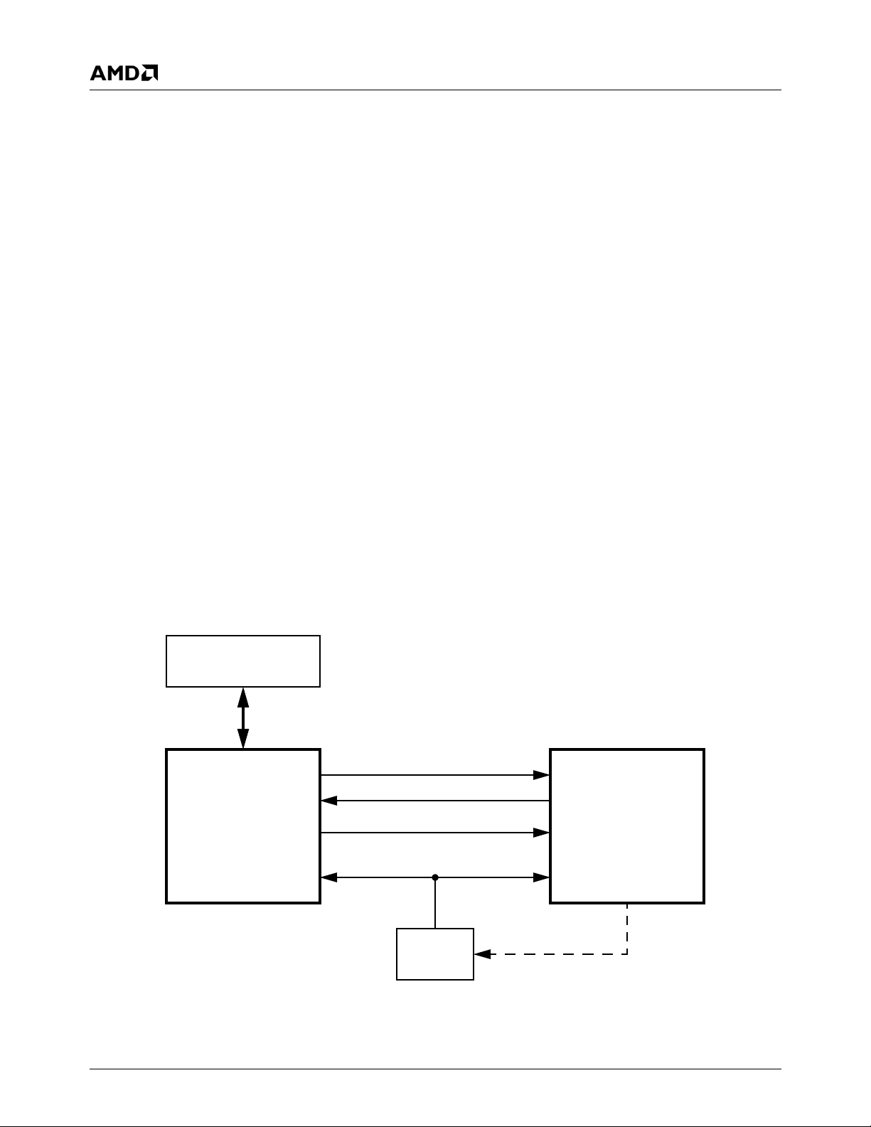
Figure 3-1 shows the recommended device interconnections. The dashed line marked SUSP_3V is intended to be
used to stop the system clocks during the 3 Volt Suspend
state; it connects to the INHIBIT pin of the system clock
generator. Designs not requiring the 3 Volt Suspend state
should not implement this connection.
3.1 GX1 Processor Serial Packet Interface
The power management logic of the GX1 processor provides the CS5530A companion with information regarding
CPU status. The majority of the system power management logic is implemented in the CS5530A, but a minimal
amount of logic is contained within the GX1 to provide
information that is not externally visible (e.g., graphics controller status).
The GX1 implements a simple serial communications
mechanism to transmit the CPU status to the CS5530A.
The GX1 accumulates CPU events in an 8-bit read-only
register, “PM Serial Packet” register (GX_BASE+Memory
Offset 850Ch), that is serially transmitted out of the GX1
every 1 to 10 µs. The transmission frequency is set with
bits [4:3] of the PM Serial Packet Control register within the
GX1. (See Table 8-1 "GX1 Processor Power Management
Serial Packet Register" on page 36 for complete bit
descriptions.)
Application Note
Revision 1.0 - April 2001 - Confidential
The packet transmitter holds the serial output pin (SERIALP) low until the transmission interval timer has elapsed.
Once the timer has elapsed, the SERIALP pin is held high
for two clocks to indicate the start of packet transmission.
The contents of the Serial Packet Register are then shifted
out starting from bit 7 down to bit 0. The SERIALP pin is
held high for one clock to indicate the end of packet transmission and then remains low until the next transmission
interval. After the packet transmission is complete, the
Serial Packet Register’s contents are cleared.
The input clock of the GX1 processor is used as the clock
reference for the serial packet transmitter.
Once a bit in the register is set, it remains set until the completion of the next packet transmission. Successive events
of the same type that occur between packet transmissions
are ignored. Multiple unique events between packet transmissions accumulate in this register. The processor transmits the contents of the serial packet only when a bit in the
Serial Packet Register is set and the interval timer has
elapsed.
The CS5530A companion device decodes the serial packet
after each transmission and performs the power management tasks related to video retrace.
SDRAM
AMD Geode™
GX1
Processor
SUSPA#
SUSP#
SERIALP (Serial Packet)
System Clock
CLOCK
GEN
SUSP_3V
Figure 3-1. Device Interconnections
AMD Geode™
CS5530A
Companion
Device
2 AMD Geode™ GX1 Processor/CS5530A Companion Device Power Management Implementations
Page 3

Application Note
Revision 1.0 - April 2001 - Confidential
4.0 Power States
This chapter is divided into two main sections describing
the GX1 processor and CS5530A companion device power
states and the SP4GX10 system platform power states.
4.1 GX1 Processor/CS5530A Companion Device Power States
The GX1 processor and CS5530A companion device have
a variety of power management features and states. In this
section, these features are described in detail from the perspective of the devices themselves. In the next major section, these same states are discussed from the system
perspective.
4.1.1 Enabling Power Management
Both the GX1 and the CS5530A have global power management enable controls that must be properly set up to
enable their power management features.
GX1: Index C2h[7] must be set to 1 for the SUSP# input
and SUSPA# output to function. Index C3h[3] must be set
to 1 if the SUSP# input is to be recognized while in SMM
mode. (See Table 8-2 "GX1 Processor Suspend Mode
Related Bits" on page 37 for bit description.)
CS5530A: F0 Index 80h[0] must be set to 1 to enable the
SUSP#/SUSPA# handshake. Other bits in this register may
also be set depending on which power management features are desired. (See Table 8-3 "CS5530A Suspend/Suspend Modulation Configuration Related Registers" on page
38 for details.)
The CS5530A has a bit located at F0 Index 96h[4], called
the “Power Savings Mode” bit. Although the data book indicates that this bit can be used to enable and disable power
management, this is not the case. The referenced bit
should always be cleared to 0, and should nev er be used to
enable or disable power management.
4.1.2 System Management Mode
The GX1 processor has an operational mode called SMM,
System Management Mode. This mode is generally
entered when the SMI# pin goes active. If active power
management is desired, then the CS5530A is programmed
at boot time to activate SMM through the SMI# pin due to
specific I/O inactivity.
SMM is also used in the passive power management
method, however, it is limited to supporting specific API
calls such as entering Sleep modes.
The GX1 processor must be enabled to recognize the
SUSP# input while in SMM. Refer to Section 4.1.1
"Enabling Pow er Management" f or enabling information.
4.1.3 Suspend-on-Halt
Suspend-on-Halt, also known as the Active Idle state, is
the most effective power-reducing feature of the GX1 processor. Suspend-on-Halt allows the system to reduce
power when the system’s OS becomes idle without introducing any delay when the system’s OS becomes active
again. The processor’s core clock is stopped in this state
and therefore, considerable power is saved in the processor.
Before entering Suspend-on-Halt, it must be enabled. Set
GX1 Index C2h[3] to 1 to allow this state to occur. (See
Table 8-2 on page 37 for bit description.)
To enter this state, the GX1 executes a HLT (Halt) instruction and asserts the SUSPA# signal in response. The operating system has control of the entry of this state because
the OS has either executed HLT or made a BIOS call to
indicate idle, and the BIOS executed the HLT instruction.
When entered, Suspend-on-Halt stops the clock to the processor core while the integrated functions (graphics, memory controller, PCI controller) are still active. The CS5530A
takes advantage of this power state by stopping the clock
to some of the internal circuitry.
There is no observational evidence that the processor has
changed operational behavior except for two things. The
GX1 draws significantly less core power and the SUSPA#
output pin is active while in this state.
The CS5530A can still make bus master requests for IDE,
audio, USB, and ISA from this state. When the CS5530A or
any other device on the PCI bus asserts REQ#, the GX1
deasserts SUSPA# for the duration of REQ# activity. Once
REQ# has become inactive and all PCI cycles have
stopped, the GX1 reasserts SUSPA#. SUSPA# remains
active until the GX1 receives an INTR or SMI event that
ends the CPU Halt condition.
4.1.4 CPU Suspend
CPU Suspend is a hardware initiated power management
state. This state is similar to Suspend-on-Halt except for its
entry and exit method; power savings is identical to Suspend-on-Halt. The GX1 enters this state in response to the
CS5530A asserting SUSP#. The GX1 asserts the SUSPA#
pin in response to indicate that the processor has entered
CPU Suspend. As in Suspend-on-Halt, the processor temporally disables CPU Suspend when there is PCI master
activity.
To prepare for this state, set GX1 Index C2h[7] to 1, which
enables the SUSP# input and the SUSPA# output. Also,
set GX1 Index C3h[3] to 1, which enables the GX1 to
respond to the SUSP# signal while in SMM.
AMD Geode™ GX1 Processor/CS5530A Companion Device Power Management Implementations 3
Page 4

Application Note
Revision 1.0 - April 2001 - Confidential
To enter Suspend, trigger a Suspend state from the
CS5530A (see Section 4.1.7 "Triggering Suspend State"
on page 6). The GX1 will complete its current cycle and
assert SUSP A# in response.
The CS5530A deasserts SUSP# when a wakeup INTR or
SMI event occurs. The Suspend Configuration register
(CS5530A F0 Index BCh) is shown in Table 8-3 on page 38
along with other related Suspend/Suspend Modulation
configuration registers.
4.1.5 Suspend Modulation
Suspend Modulation is a derivative of the On and Suspend
states and works by asserting and deasserting the SUSP#
pin to the CPU for a configurable period and duty cycle. By
modulating the SUSP# pin, an effective reduction in frequency is achieved. Certain processing activities (SMI#,
interrupts, and VGA activity) can be monitored by the
CS5530A to temporarily interrupt Suspend Modulation for a
programmable amount of time.
Suspend Modulation is the system power management
choice of last resort. However, it is an excellent choice for
thermal management. If the system i s expected to operate
in a thermal environment where the processor co uld overheat, then Suspend Modulation can be used to reduce
power consumption in the overheated condition and thus
reduce the processor’s temperature.
When used as a power management state, Suspend Modulation works by assuming that the processor is idle unless
external activity indicates otherwise. This approach effectively slows down the processor until external activity indicates a need to run at full speed, thereby reducing power
consumption.
Suspend Modulation serves as the primary CPU power
management mechanism when APM or some other power
management software strategy is not present. It can also
act as a backup for situations where the power management scheme does not correctly detect an Idle condition in
the system.
In order to provide high-speed performance when needed,
the SUSP# pin modulation can be temporarily disabled any
time system activity is detected. When this happens, the
processor is “instantly” converted to full speed for a programmed duration. System activities in the CS5530A are
defined in hardware as: any unmasked IRQ, accessing
Port 061h, SMI, and/or accessing the graphics controller.
Since the graphics controller is integrated in the GX1, the
indication of graphics activity is sent to the CS5530A via
the serial link (see Section 3.1 "GX1 Processor Serial
Packet Interface" on page 2) and is automatically decoded.
Graphics activity is defined as any access to the VGA register space, the VGA frame buffer, the graphics accelerator
control registers and the configured graphics frame buffer.
The automatic speedup events (IRQ, SMI, and/or graphics)
for Suspend Modulation should be used together with software-controlled speedup registers for major I/O events
such as any access to the floppy disk controller, hard disk
drive, or parallel/serial ports, since these are indications of
major system activities. When major I/O events occur, Suspend Modulation can be temporarily disabled using the
procedures described in the following subsections.
Bus master internal (Ultra DMA/33, Audio, USB, or ISA) or
external requests do not directly affect the Suspend Modulation programming.
4.1.5.1 Suspend Modulation for Thermal
Management
The best use of Suspend Modulation is for thermal management. If the system exceeds temperature limits in
extreme conditions, then thermal management by use of
Suspend Modulation can be easily and effectively used to
reduce system cost by eliminating fans and possibly also
heatsinks. Howev er, if maximum performance is required in
all conditions then Suspend Modulation should not be
used, since invoking Suspend Modulation imposes a performance penalty.
Using an external circuit based on Nati onal Semiconductor’s LM84 temperature sensor or similar device, the
CS5530A can monitor the temperature of the system
and/or CPU, and assert the SMI# pin if the system or CPU
exceeds a predefined high limit. The power management
SMM handler then enables Suspend Modulation, allowing
the processor or system to cool off. When the temperature
drops back below a predefined low limit, the CS5530A
again asserts the SMI# pin. The power management SMM
handler disables Suspend Modulation and nor mal operation resumes.
4.1.5.2 Suspend Modulation for Power Management
Suspend Modulation can also be used for a crude method
of power management. The CS5530A monitors I/O activity
and when that monitoring indicates inactivity, the CS5530A
asserts the SMI# pin. The power management SMM handler enables Suspend Modulation. When I/O activity picks
up, the SMI# pin is asserted again and the power management SMM handler exits Suspend Modulation and normal
operation resumes.
4 AMD Geode™ GX1 Processor/CS5530A Companion Device Power Management Implementations
Page 5

Application Note
Revision 1.0 - April 2001 - Confidential
4.1.5.3 Configuring Suspend Modulation
Control of the Suspend Modulation feature is accomplished
using the CS5530A’s Suspend Modulation OFF Count
Register, Suspend Modulation ON Count Register, and
Suspend Configuration Register (F0 Index 94h, 95h, and
96h, respectively). The CS5530A Power Management
Enable Register 1 (F0 Index 80h) contains the enables for
the individual activity speedup timers.
Bit 0 of the Suspend Configuration Register (F0 Index 96h)
enables the Suspend Modulation feature. Bit 1 controls
how SMI events affect the Suspe nd Modulation feature. In
general this bit should be set to a 1, which causes SMIs to
disable Suspend Modulation until it is re-enabled by the
SMI handler.
The CS5530A Suspend Modulation OFF and ON Count
Registers (F0 Index 94h and 95h) control two 8-bit
counters that represent the number of 32 µs inter vals that
the SUSP# pin is asser ted and then deasserted to the processor. These counters define a ratio that is the effective
frequency of operation of the system while Suspend Modulation is enabled.
F
= F
eff
GX86
x
Off Count
On Count + Off Count
The IRQ and Video Speedup Timer Count registers
(CS5530A F0 Index 8Ch and 8Dh) configure the amount of
time that Suspend Modulation is disabled when the respective events occur.
4.1.6 3 Volt Suspend
3 Volt Suspend is a non-operational state, and is a lower
system power state than CPU Suspend. This state is usually used to put the system into a deep sleep to conserve
power and still allow the user to resume where they left off.
In a system designed to take full advantage of this mode
(such as the SP4GX10), not only is the processor in the
Suspend mode, but the graphics pipeline is disabled, the
system SDRAMs are in a low-power self refresh state, and
the processor’s core clock has been stopped. Figure 3-1
"Device Interconnections" on page 2, shows (as a dashed
line) the connection required between the CS5530A and
the system clock generator to allow system clock stopping.
To prepare to enter this state:
1) Set the CLK_STP bit in the GX1 PM_CNTRL_CSTP
register (GX_BASE+Memory Offset 8508h[0] = 1).
2) Set the CPU Clock Stop bit in the CS5530A Clock
Stop Control Register (F0 Index BCh[0] = 1).
3) Turn off the graphics pipeline (GX_BASE+Memory
Offset 8304h[0] = 0).
The only function of the CLK_STP bit in the GX1 is to force
the memory controller in the GX1 to put the SDRAMs into a
self refresh mode upon acknowledgement of a SUSP#
input. If CLK_STP is set and the graphics pipeline is still
active, then the SUSP# is ignored and 3 Volt Suspend is
not entered.
4.1.5.4 SMI Speedup Disable
If the Suspend Modulation feature is being used for CPU
power management, the occurrence of an SMI disables the
Suspend Modulation function so that the system operates
at full speed while in SMM. There are two methods used to
invoke this via bit 1 of the Suspend Configuration Register.
If F0 Index 96h[1] = 0: Use the CS5530A IRQ Speedup
Timer (F0 Index 8Ch) to temporarily disable Suspend Modulation when an IRQ occurs.
If F0 Index 96h[1] = 1: Disable Suspend Modulation when
an SMI occurs until a read to the SMI Speedup Disable
Register (F1BAR+Memory Offset 08h) occurs.
The CS5530A SMI Speedup Disable Register prevents Virtual System Architecture (VSA) technology software from
entering Suspend Modulation while operating in SMM. The
data read from this register can be ignored. If the Suspend
Modulation feature is disabled, reading this I/O location has
no effect. Table 8-3 on page 38 shows the bit formats of the
Suspend Modulation related registers.
Upon programming completion, trigger a Suspend state
from the CS5530A (see Section 4.1.7 "Triggering Suspend
State" on page 6). A SUSP#/SUSPA# handshake cycle will
occur, and then the 3 V olt Suspend state will occur . When 3
Volt Suspend is entered, the GX1 memor y controller puts
the SDRAMs in self refresh mode. Once SUSPA# has gone
active, the SYSCLK input pin to the GX1 can also be
stopped via the INHIBIT control on the clock generator.
The CS5530A supports the stopping of the CPU and system clocks in the 3 Volt Suspend state. The CS5530A
asserts the SUSP_3V pin after it has gone through the
SUSP#/SUSPA# handshake with the GX1. The SUSP_3V
pin is a state indicator, indicating that the system is in a
low-activity state. This indicator can be used to put the system into a low-power state (the system clock can be turned
off). The CS5530A’s SUSP_3V output pin is intended to be
connected to the output enable of a clock generator or
buffer chip, so that the clocks to the GX1 and the CS5530A
(and most other system devices) can be stopped.
AMD Geode™ GX1 Processor/CS5530A Companion Device Power Management Implementations 5
Page 6

Application Note
Revision 1.0 - April 2001 - Confidential
The CS5530A continues to decrement all of its internal
device timers and respond to external SMI interrupts after
the input clock has been stopped, as long as the external
32 KHz clock on pin AE3 [CLK_32K] continues to oscillate.
(Note that the SP4GX10 platform does not include this 32
KHz oscillator. The oscillator must be added in order to
support the 3 Volt Suspend mode). Any SMI event or
unmasked interrupt pin causes the CS5530A to deasser t
the SUSP_3V pin, thereby restarting the system clocks.
(See Section 5.1.10 "CS5530A Companion Device Issues"
on page 27 for details on how to use interrupts to wakeup
the system.) As the CPU or other device might include a
PLL, the CS5530A holds SUSP# active for a pre-programmed period of delay (the PLL re-sync delay) that varies from 0 to 15 ms to allow the PLL to resynchronize. After
this period has expired, the CS5530A deasser ts SUSP#,
and the GX1 responds by deasserting SUSPA#, stopping
Suspend. SMI# is held active for the entire period, so that
the GX1 reenters SMM when the clocks are restarted.
Note: The SUSP_3V pin can be active either high or low.
The pin is an input during POR, and is sampled to
determine its inactive state. This allows a designer
to match the active state of SUSP_3V to the inactive state for a clock driver output enable by using
either a pull-up or a pull-down resistor.
While in the 3 Volt Suspend state the GX1 processor will
not respond to anything except the deassertion of SUSP#,
as long as SYSCLK has been restarted.
4.1.6.1 Hybrid 3 Volt Suspend States
Since the 3 Volt Suspend state control registers reside in
two separate parts, it is possible to create hybrid states by
setting the bits in different configurations. If CLK_STP in
the GX1 PM_CNTRL_CSTP register is not set, then a 3
Volt Suspend state will still occur, except that the SDRAMs
will not be put into a self refresh mode. This implies that the
GX1 SYSCLK input may not be stopped, for doing so
would cause loss of the SDRAM contents.
4.1.7 Triggering Suspend State
The preceding discussions of Suspend and 3 Volt Suspend
have referred to the phrase, “trigger a Suspend state”.
Suspend-On-Halt is triggered by writing a HLT command to
the GX1 processor. A Suspend state is triggered by writing
to one of two CS5530A Function 0 (F0) registers, Index
AEh or AFh. Depending on the state of certain register bits,
these write commands trigger a Suspend state as
described in the methods below. Before using either of
these methods, the SUSP#/SUSPA# handshake must be
enabled. To enable the handshake, set CS5530A F0 Index
80h[0] = 1.
Method 1: F0 Index AEh: Software CPU
Suspend Command (Write Only):
If bit 0 in the CS5530A Clock Stop Control Register is set
low (F0 Index BCh[0] = 0) and all SMI status bits are 0, a
write to this register causes a SUSP#/SUSPA# handshake
with the CPU, placing the CPU in a Suspend state. The
data written is irrelevant. Once in this state, any unmasked
IRQ or SMI releases the CPU Suspend condition.
If F0 Index BCh[0] = 1, writing to this register invokes a 3
Volt Suspend. The SUSP_3V pin is asserted after the
SUSP#/SUSPA# halt. Upon a Resume event (see Note),
the PLL delay programmed in the F0 Index BCh[7:4] is
invoked, allowing the clock chip and CPU PLL to stabilize
before deasserting the SUSP# pin.
Note: If the system clocks are stopped, the external
IRQ4, IRQ3, and IRQ1 pins, when enabled
(CS5530A F3BAR+Memory Offset 1Ah[4:3]), are
the only IRQ pins that can be used as a Resume
event. If GPIO2, GPIO1, and GPIO0 are enabled
as an external SMI source (CS5530A F0 Index
92h[2:0]), they too can be used as a Resume
event. No other CS5530A pins can be used to
wakeup the system from Suspend when the clocks
are stopped. As long as the 32 KHz clock remains
active, internal SMI events are also Resume
events.
See Section 5.1.10 "CS5530A Companion Device
Issues" on page 27 for details on how to use IRQs
and GPIOs to wakeup the system.
Method 2: Function 0 Index AFh: Software CPU Stop
Clock Suspend (Write Only):
A write to this register causes a SUSP#/SUSPA# handshake with the CPU, placing the CPU in a low-power state.
Following this handshake, the SUSP_3V pin is asserted.
The SUSP_3V pin is intended to be used to stop all system
clocks.
Upon a Resume event (see Note), the SUSP_3V pin is
deasserted. After a slight delay, the CS5530A deasserts
the SUSP# signal. Once the clocks are stable, the processor deasserts SUSPA# and system operation resumes.
Note: If the system clocks are stopped, the external
IRQ4, IRQ3, and IRQ1 pins, when enabled
(CS5530A F3BAR+Memory Offset 1Ah[4:3]), are
the only IRQ pins that can be used as a Resume
event. If GPIO2, GPIO1, and GPIO0 are enabled
as an external SMI source (CS5530A F0 Index
92h[2:0]), they too can be used as a Resume
event. No other CS5530A pins can be used to
wakeup the system from Suspend when the clocks
are stopped.
See Section 5.1.10 "CS5530A Companion Device
Issues" on page 27 for details on how to use IRQs
and GPIOs to wakeup the system.
6 AMD Geode™ GX1 Processor/CS5530A Companion Device Power Management Implementations
Page 7

Application Note
Revision 1.0 - April 2001 - Confidential
4.2 System Platform Power States
The discussion of system power states that follows is
generic and may apply to any system platform based on
the AMD Geode™ processor. References to letter-named
modes (e.g., Mode C) are to specific states of the AMD’s
Geode™ SP4GX10 system platform. These letter-named
modes are described in detail in the Section 5.0 on page
12. The terms used in this section: “Off”, “Doze”, “Standby”,
and “Suspend”, are industry-stan dard term s and are deliberately used here for persons familiar with power management techniques.
4.2.1 Mechanical Off State
The Mechanical Off state is entered and left by a mechanical means such as turning off an external AC power switch,
or disconnecting the power cord or battery. In the Mechanical Off state no electrical current is applied to the circuitry.
The OS must be fully restarted to return to the Working
state unless a Save-to-Disk or Save-to-RAM operation was
performed prior to entering the Mechanical Off state. No
hardware context is maintained in the circuitry except for
data in the battery backed CMOS RAM (if present). The
power consumption in the Mechanical Off state is zero.
4.2.2 Off State
In the Off state the SP4GX10 consumes minimal power.
The CPU is powered off and no code is executing. The Off
state is entered via hardware or software control. The Off
state is entered under hardware control by depressing the
on/off switch on the board (a four second hold delay may
be required depending upon SuperI/O setup). The Off state
can be entered under software control through the appropriate BIOS call or by writing the appropriate SuperI/O register directly. Typically the BIOS abstraction layer is
employed.
The system context in the Off state is not maintained so the
OS must be fully restarted to return to the Working state
unless a Save-to-Disk or Save-to-RAM oper a tion w a s completed prior to entering the Off state.
Return to the Working state from the Off state is accomplished by activation of the wake inputs. These wake inputs
include: activation of the on/off button, PME# activation via
Wake-on-LAN, activation of the RI# (ring) input, or activation of the RTC (real-time clock) alarm. Note that all of
these wake events assume the presence of the National
Semiconductor PC97317 SuperI/O. Return to the Working
state from Off requires approximately the same amount of
time as a return from the Mechanical Off state. The Off
state is the typical Off state of a system.
4.2.3 Working State
In the Working state, the system is operational and user
mode (application) threads are executing. In this state, system elements and peripherals may have their power
dynamically managed based on system operation. The
system design allows the user to select various performance versus power operation modes and profiles. The
system responds to external events in real-time. There are
several variants of the Working state. Note that the implementation modes (Modes A-I) described in Section 5.1
"Mode Programming" on page 12 represent the implementation on the SP4GX10 system platform. It is expected that
there would be some modification of these operational
states to fit a specific system design.
4.2.3.1 Full-On Mode
The Full-On mode is the full power operating mode of the
system when in the Working state. This mode is the same
as Mode A. All devices are fully powered and operating at
full speed. All component clocks are present and running at
full speed. The Full-On mode is entered upon initial system
power up from the Mechanical Off or Off state and is also
entered in response to a trigger event from one of several
sources if the system is in one of the power conservation
modes of the Working State.
When the Full-On mode is entered, the Doze timers are
enabled if the system is setup to use Doze mode hardware
timers. When the Doze mode timers elapse, the system
enters the first level of power conservation.
4.2.3.2 Doze Mode
The Doze mode is the first level of power conservation of
the system when in the Working state. The system is in
Suspend Modulation (Mode B) or Active Idle (Mode C),
depending on the method of entry, when in Doze mode.
While operating in Doze mode there is virtually no
decrease in end-user perceivable performance of functionality. In Doze mode, power savings is achieve d through the
use of Suspend Modulation to the GX1 and/or by entering
the Suspend-On-Halt state. Both states may be present at
the same time. While the primary means of power saving is
achieved through the use of Suspend Modulation, the system design may also allow selective, autonomous powering
down of non-critical peripherals if they are not accessed.
The important consideration is user-observed latency. In
Doze mode the latency must be kept to a minimum. There
are two methods for en te ring Do ze mode.
AMD Geode™ GX1 Processor/CS5530A Companion Device Power Management Implementations 7
Page 8

Application Note
Revision 1.0 - April 2001 - Confidential
The first method of Doze mode entry is under software
control through the execution of the HLT instruction. In a
simple single threaded application it may be possible to
craft the design so as to include the HLT opcode directly
within the application executable. In operation, the system
will execute to the HLT instruction and remain there until an
INTR (Interrupt) or SMI# (System Management Interrupt) is
sensed. In a more sophisticated system with multiple
threads running, the task manager can include the HLT
instruction when the system idle thread is called. Alternatively, the system idle thread can call back to the BIOS with
an APM-aware CPU-idle call.
The second method of Doze mode entry occurs when the
hardware (such as an event timer) signals a time-out. This
event will typically signal through the generation of an SMI.
The SMM handler responds by enabling Suspend Modulation. Suspend Modulation effectively reduces the CPU
power consumption by asserting and de-asserting the
SUSP# input to the GX1. The duty cycle of Suspend Modulation is fully programmable, howeve r, aggressive settings
are recommended. The system can be setup to override
the Suspend Modulation when critical events such as interrupts (INTR) or system management interrupts (SMI#)
must be processed. This override is referred to interrupt
speedup and insures low latency when processing critical
operations such as mouse movement or keystrokes.
It is important to note that the Suspend Modulation state
can also be entered in response to a thermal event. If the
system thermal sensor detects that the temperature has
risen above an established threshold, a thermal activity
SMI is signaled and the SMM handler enables Suspend
Modulation in response. When the over-temperature condition is no longer present, the system is returned to the FullOn mode, assuming no further time-outs have occurred.
When Doze mode is entered, the Standby mode timers are
enabled. Exit from Doze mode to the Full-On mode occurs
upon activation of an interrupt or SMI. If processing of the
event does not cause a reload of the Doze mode timer (and
therefore the Standby mode timer), then Doze mode is reentered upon completion of the processing of the event.
Doze mode can also be exited to the Standby mode if the
Standby mode timers elapse or if software commands an
entry to the Standby mode.
4.2.3.3 Standby Mode
The Standby mode is the second level of power conservation for the SP4GX10 platform. This mode is the same as
Mode D or E depending on the system implementation.
Higher user response latency and performance degradation are evident following entry into the Standby state. The
Geode devices are in the “CPU Suspend” state. The LCD
panel and backlight are disabled but all other peripherals
are operational in the implementation of Standby mode on
the SP4GX10 platform. It is possible to autonomously,
selectively power down additional peripherals in this state
using the precepts outlined in the subsections of Section
6.0 "Peripheral Power Management" of this application
note. The specific implementation is at the discretion of the
system designer. It is important to note that the complexity
of the wakeup logic and the system response latency
increase if additional devices are powered down in Standby
mode, but the power savings may justify the effort.
Standby mode is entered when the appropriate timer
elapses and generates an SMI to signal a Standby mode
time-out. The SMM handler responds by placing the system into Mode E or F. The mode used is selectable by the
system designer. In Mode E the GX1 is in Suspend state
and the LCD is disabled. In Mode F, the GX1 is Suspended
and the graphics interface is fully disabled.
Significant power savings are realized by placing the GX1
in the CPU Suspend state and disabling the graphics interface. The system still responds to system interrupts and
SMIs and processes them without enabling the display.
This allows timer ticks and various system management
events to be processed while maintaining a reduced power
consumption state. The interrupt speedup mechanism (see
Section 4.1.5.4 "SMI Speedup Disable" on page 5) is
employed in order to process system interrupts while in the
Standby mode. User or application generated interrupts
such as keystrokes, mouse movements, or disk accesses
return the system to the Full-On mode.
When Standby mode is entered, the Suspend mode timers
are enabled. Exit from Standby mode to the Full-On mode
occurs upon activation of an interrupt or SMI. If processing
of the event does not cause a reload of the Standby and
Doze mode timers, then Standby is re-entered upon completion of the processing of the event. Standby mode can
also be exited to the Suspend mode if the Suspend mode
timers elapse or if software commands an entry to the Suspend mode.
8 AMD Geode™ GX1 Processor/CS5530A Companion Device Power Management Implementations
Page 9

Application Note
Revision 1.0 - April 2001 - Confidential
4.2.3.4 Suspend Mode
The Suspend mode is the third and the most aggressive
power conservation mode. This mode is the same as Mode
H or Mode I, depending on the degree to which clock-stopping has been implemented in the hardware. User
response latency and performance degradation are evident
following entry into the Suspend mode. The GX1 and
CS5530A are in the 3 Volt Suspend state. All system
peripherals are disabled in this mode, but can be quickly
re-enabled and returned to an operational state. Suspend
mode results in the highest level of system power conservation while still maintaining the ability to quickly restore
the system to the Full-On mode. All peripherals are still
powered in this mode, only operation (and possibly clock
inputs) is inhibited.
Suspend mode is entered when the appropriate timer
elapses and generates an SMI to signal a Suspend mode
time-out or when software specifically commands a Suspend mode entry, The SMM handler responds to the SMI
by placing the system into Mode G or I. The mode used is
selectable by the system designer; detailed design choices
must be made to support halting various system clocks. In
Mode G the system is suspended but all clocks are maintained. In Mode I, the system is suspended and the external clock inputs to the system are halted. Mode I
represents the lowest possible power state while maintaining relatively low latency of return to the Full-On state.
The system must contain software specifically written to
perform the Save function. It is beyond the scope of this
application note to present the design of a system capable
of performing Save-to-Disk or Save-to-RAM, including the
required software. This note simply points out the special
features of the GX1 and CS5530A that enable these functions.
4.2.4.2 Shadow Registers
The CS5530A contains a set of “shadow registers” that
facilitate saving certain types of system state information.
These registers (see Table 8-4 "Power Management
Shadow Registers" for bit descriptions) provide a means to
record the status and setup for each standard device in any
system;
• DMA Controller
• Programmable Interval Timer (PIT)
• Programmable Interrupt Controller (PIC)
• Real-Time Clock (RTC)
The PC/AT compatible floppy port is not part of the
CS5530A. If a floppy is attached on the ISA bus by a
SuperI/O or by some other means, some of the FDC registers are shadowed in the CS5530A. The FDC shadow registers should also be saved during the Save-to-RAM or
Save-to-Disk operation.
4.2.4 Save-to-Disk/Save-to-RAM
The GX1 and the CS5530A have the capability to save
their complete state to either non-volatile (NV) RAM or to
disk. Once this information has been saved, the system
can be turned off entirely. When powered back on, the system can be returned exactly back to the state it was in
when the save process began. This means that the system
does not have to be rebooted in the traditional sense.
4.2.4.1 The Saving Medium
The medium to which the information is saved must be
non-volatile, meaning, the memory contents must remain
unchanged when power is removed and reapplied. Hard or
floppy disks are inherently non-volatile; RAM can be made
non-volatile by design. A small bank of static RAM could be
added to the design, because static RAM does not require
refresh cycles and thus would be very low power in the Off
state. Dynamic RAM could also be used, provided it can be
placed into a self refresh state. In both cases, power must
be continuously applied to the RAM, even (especially)
when system power is off. Of course, precautions must be
taken in the system design to make sure that there is sufficient space on the saving medium to store the state information.
4.2.5 System State Transitions
Designing a system for power management is best done
using a state transition diagram. The designer should first
identify which power management states the system being
designed should support, and then identify what actions
should cause transitions between the states.
AMD Geode™ GX1 Processor/CS5530A Companion Device Power Management Implementations 9
Page 10
Application Note
Revision 1.0 - April 2001 - Confidential
4.2.5.1 Basic Power Management States
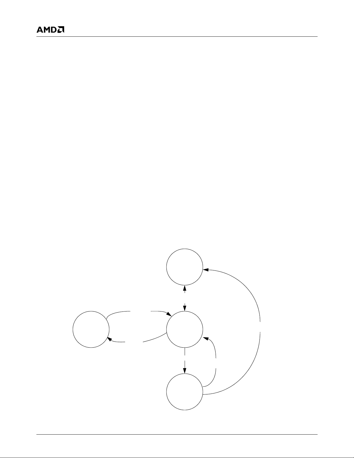
Figure 4-1 illustrates a system with basic power management features. The system has four states, two of them
being power management states, and the other two are the
basic On and Off states that any system will have.
The system shown will transition to either Suspend Modulation or to Mode D, which is a form of Suspend (see Section 4.1.5 "Suspend Modulation").
4.2.5.2 Advanced Power Management States
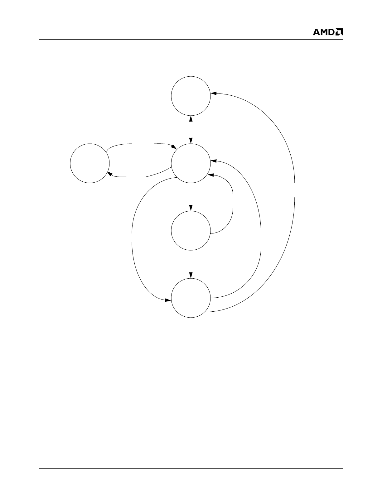
Figure 4-2 on page 11 illustrates a more complex system,
whose hardware is configured similar to that shown in Figure 3-1 "Device Interconnections" on page 2. This system
supports 3 Volt Suspend (Mode I) in addition to simple Suspend and Suspend Modulation. Note the presence of a button-push to immediately put the system into 3 Volt
Suspend.
APM Support
The GX1 and CS5530A provide APM-compliant power
states. The “APM Standby” state is equivalent to the Suspend state. The “APM Suspend” state is equivalent to the 3
V olt Suspend state . The system BIOS (XpressR OM) for the
SP4GX10 contains an APM-compliant BIOS interface.
It is not the purpose of this discussion to give any details on
interfacing to the SP4GX10 XpressROM BIOS, however, a
few general comments regarding APM are made.
Some IA systems rely solely on an APM (Advanced Power
Management) driver for DOS, Microsoft
®
Windows® 95/98,
and other operating systems for enabling the operating
system to power-manage the CPU. APM provides several
services that enhance the system power management by
determining when the CPU is idle. For the CPU, APM is
theoretically the best approach but there are some drawbacks:
• APM is an OS-specific driver, and may not be available
for some operating systems.
• Application support is inconsistent. Some applications in
the foreground may prevent Idle calls.
• APM does not help with Suspend determination or
peripheral power management.
The CS5530A provides two entry points for APM support:
• Software CPU Suspend control via the CPU Suspend
Command Register (F0 Index AEh).
• Software SMI entry via the Software SMI Register (F0
Index D0h). This allows the APM BIOS to be part of the
SMI handler.
The bit formats for these registers are shown in Table 8-3
"CS5530A Suspend/Suspend Modulation Configuration
Related Registers" on pag e 38 .
Suspend
Modulation
(Mode B)
Off
On/Off
Button
IRQs,
Video Speedup
Full-On
(Mode A)
Timer
Timer, Button
SUSP#/
SUSPA#
(Mode D)
Button, any SMI,
Unmasked IRQ
Figure 4-1. Basic Power Management State Transitions
On/Off
Button
10 AMD Geode™ GX1 Processor/CS5530A Companion Device Power Management Implementations
Page 11
Application Note
Revision 1.0 - April 2001 - Confidential
Suspend
Modulation
(Mode B)
IRQs,
Video Speedup
Timer
Off
On/Off
Button
Full-On
(Mode A)
Timer
Any SMI,
Unmasked IRQ
On/Off
Button
SUSP#/
Button
SUSPA#
(Mode E)
Timer
SUSP#/
SUSPA# and
SUSP_3V
(Mode I)
Any SMI,
Unmasked IRQ
Figure 4-2. Advanced Power Management State Transitions
AMD Geode™ GX1 Processor/CS5530A Companion Device Power Management Implementations 11
Page 12
Revision 1.0 - April 2001 - Confidential
5.0 SP4GX10 System Platform Working State Modes
Nine modes for the Working state, labeled A through I,
have been defined for the SP4GX10 system platform; however, many additi onal states are possible when all combinations of peripheral device power states (see Section 6.0
"Peripheral Power Management" on page 30) are considered. Modes A through I describe system-wide effects of
power state changes in the Geode devices (the GX1 processor and CS5530A companion) and do not reflect any
changes in the power status of peripheral devices.
5.1 Mode Programming
The following discussion provides details of each of the
defined Modes A through I. Each mode is briefly discussed
and the GX1/CS5530A register setups are provided.
5.1.1 Mode A: Full-On
This is the fully on and normal state. All power planes are
on and all clocks are running.
Application Note
Modes involving 3 Volt Suspend require that a 32 KHz
oscillator be added to the SP4GX10 board; these are
modes F through I inclusive.
The modes are:
• Mode A: Full-On.
• Mode B: Suspend Modulation.
• Mode C: Suspend-on-Halt (Active Idle).
• Mode D: SUSP#/SUSPA#.
• Mode E: SUSP#/SUSPA# with some clock stopped
(using PM PAL).
• Mode F: SUSP#/SUSPA# with the PM_CNTRL_CSTP
register set in the GX1 for 3 Volt Suspend
(GX_BASE+Memory Offset 8508h[0] = 1).
• Mode G: SUSP#/SUSPA# and SUSP_3V active with all
clocks still running.
• Mode H: SUSP#/SUSPA# and SUSP_3V active with
some PCI clocks stopped.
• Mode I: SUSP#/SUSPA# and SUSP_3V active with all
clocks stopped.
5.1.2 Mode B: Suspend Modulation
This is the first level of power management, and must have
a very quick response latency so that it can be entered very
quickly. The GX1 processor enters Suspend Modulation if
there is no activity after a certain amount of time. Any interrupt and/or SMI causes the system to exit from this state.
• Mode B device status:
— GX1: Suspend Modulation
— CS5530A: Suspend Modulation
— Main memory: Active
— Other devices: Active
• Mode B entry event:
— Timer expiration (e.g., CS5530A GP Timer 1)
— Thermal activity (if applicable)
• Mode B exit event:
— Any unmasked Interrupts
— Any asserted SMI
—NMI
— Accessing the video port
— Video activity (any access to the VGA regis ter space,
the VGA frame buff er, the graphic accelerator control
register and the configured graphic frame buffer)
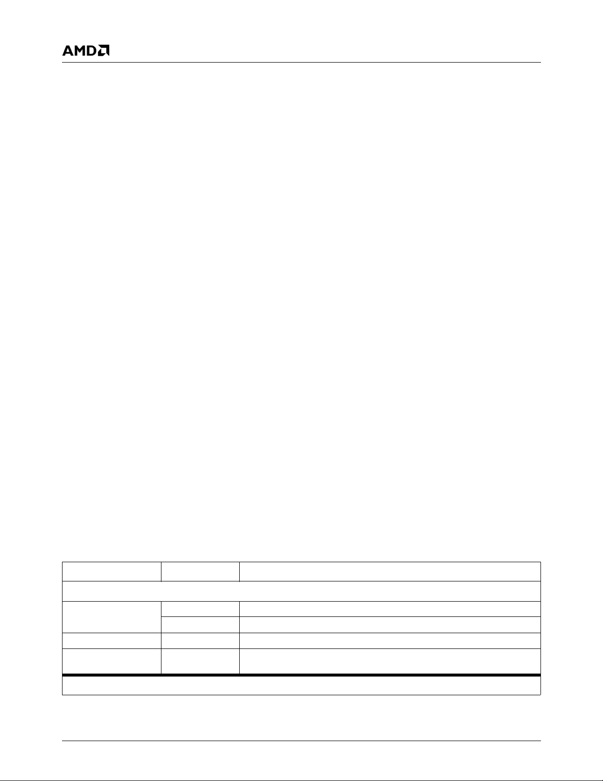
Table 5-1 provides the required register programming for
Mode B.
Table 5-1. Mode B Register Programming
Register Setting Description
GX1 Processor
Index C2h (CCR2) Bit 7 = 1 Suspend Pins (SUSP# and SUSPA#) (1 = Enable)
Bit 3 = 0 Suspend-on-Halt
Index 3Ch (CCR3) Bit 3 = 1 Allow Suspend in SMM Mode (1 = SUSP# recognized in SMM mode)
GX_BASE+Memory
Offset 8508h
CS5530A Companion Device
12 AMD Geode™ GX1 Processor/CS5530A Companion Device Power Management Implementations
Bit 0 = 0 Clock Stop (0 = Suspend Refresh Mode): Core stopped, the clocks to the
memory and display controller remain active
Page 13
Application Note
Revision 1.0 - April 2001 - Confidential
Table 5-1. Mode B Register Programming (Continued)
Register Setting Description
F0 Index 80h Bit 4 = 1 Video Speedup (1 = Enable)
Bit 3 = 1 IRQ Speedup (1 = Enable)
Bit 0 = 1 Global Power Management (1 = Enable)
F0 Index 88h
See Footnote
F0 Index 89h GPT1 Control
Bit 7 = 1 Timebase (1 = 1 ms)
Bit 6 = 0 Re-trigger on UDEF3 (0 = Disable)
Bit 5 = 0 Re-trigger on UDEF2 (0 = Disable)
Bit 4 = 0 Re-trigger on UDEF1 (0 = Disable)
Bit 3 = 1 Re-trigger on Keyboard/Mouse (1 = Enable)
Bit 2 = 1 Re-trigger on Parallel/Serial (1 = Enable)
Bit 1 = 1 Re-trigger on Floppy (1 = Enable)
Bit 0 = 1 Re-trigger on Primary HDD (1 = Enable)
F0 Index 8Ah 00h GP Timer 2 Count
F0 Index 8Bh GPT2 Control
Bit 7 = 0 Re-trigger on Secondary HDD (0 = Disable)
Bit 6 = 0 VGA Timer Base (0 = 1 ms)
Bit 5 = 0 GPT2 shift (0 = No shift)
Bit 4 = 0 GPT1 shift (0 = No shift)
Bit 3 = 1 Timebase for GPT2 (1 = 1 ms)
Bit 2 = 0 Re-trigger on GPT2 (0 = Disable)
Bits [1:0] = 00 Reserved
F0 Index 8Ch See Description
Column
F0 Index 8Dh See Description
Column
F0 Index 94h See Description
Column
F0 Index 95h See Description
Column
F0 Index 96h Bit 1 = 1 Disable Suspend Modulation when an SMI occurs (1 = Yes)
Bit 0 = 1 Suspend Modulation (1 = Enable)
F1BAR+Memory
Any Value Read to re-enable Suspend Modulation at every SMI exit point
Offset 08h
1
GP Timer 1 Count
IRQ Speedup Timer Count (timer load value): 1 ms,
a typical value = 2 to 4 ms
Video Speedup Timer Count (timer load value): 1 ms,
a typical value = 2 to 4 ms
Suspend Signal Deasserted Count (8-bit counter): 32 µs
Suspend Signal Asserted Count (8-bit counter): 32 µs
1. The values for GPT1 and GPT2 are selected by the system designer. This value should be the maximum length of time
(in either seconds or milliseconds, depending on the counter’s timebase) that any device in the re-trigger list may remain
inactive before a power management state is triggered.
AMD Geode™ GX1 Processor/CS5530A Companion Device Power Management Implementations 13
Page 14
Application Note
Revision 1.0 - April 2001 - Confidential
5.1.3 Mode C: Suspend-on-Halt Instruction
This is the second level of power management. The GX1
enters this mode if a HL T (Halt) instruction is ex ecuted. The
SUSPA# pin is active while in this state without asserting of
SUSP#.
When entered, Suspend-on-Halt stops the clocks to the
processor core while the integrated functions (graphics,
memory controller, PCI controller) are still active.
• Mode C entry event:
— APM call
— Execute a HLT instruction
• Mode C exit event:
— Any unmasked Interrupts
— Any asserted SMI
—NMI
— Accessing the video port
— Video activity (any access to the VGA regis ter space,
• Mode C device status:
— GX1: Active Idle
the VGA frame buff er, the graphic accelerator control
register and the configured graphic frame buffer)
— CS5530A: Active
— Main memory: Active
— Other devices: Active
Table 5-2 provides the required register programming for
Mode C.
Table 5-2. Mode C Register Programming
Register Setting Description
GX1 Processor
Index C2h (CCR2) Bit 7 = 1 Suspend Pins (SUSP# and SUSPA#) (1 = Enable)
Bit 3 = 1 Suspend-on-Halt (1 = Enable)
GX_BASE+Memory
Offset 8508h
Bit 0 = 0 Clock Stop (0 = Suspend Refresh Mode): Core stopped, the clocks to the
memory and display controller remain active
14 AMD Geode™ GX1 Processor/CS5530A Companion Device Power Management Implementations
Page 15
Application Note
Revision 1.0 - April 2001 - Confidential
5.1.4 Mode D: SUSP#/SUSPA#
The GX1 enters this mode if the GP Timer 1 in the
CS5530A expires. Upon expiration, the BIOS writes the
CS5530A CPU Suspend Command register (F0 Index
AEh) to cause a SUSP#/SUSPA# handshake. The SUSP#
pin is asserted by the CS5530A and the GX1 responds by
asserting the SUSPA# pin to indicate that the processor
has entered Suspend. If USB is enabled, the SUSPA# signal is deasserted every 1 ms due to the 1 ms REQ1# signal
from the CS5530A (USB controller).
SUSP#/SUSPA is similar to Suspend-on-Hal t except for its
entry and exit method in terms of hardware protocol.
• Mode D device status:
• Mode D entry event:
— Expiration of GP Timer 1
• Mode D exit event:
— Any unmasked interrupts (e.g., keyboard or mouse
activity)
— Any asserted SMI
—NMI
— Accessing the video port
— Video activity (any access to the VGA regis ter space,
the VGA frame buff er, the graphic accelerator control
register and the configured graphic frame buffer)
Table 5-3 on page 15 provides the required register programming for Mode D.
— GX1: Suspend
— CS5530A: Suspend
— Main memory: Active
— Other devices: Active
Table 5-3. Mode D Register Programming
Register Setting Description
GX1 Processor
Index C2h (CCR2) Bit 7 = 1 Suspend Pins (SUSP# and SUSPA#) (1 = Enable)
Bit 3 = X Suspend-on-Halt −−> Don’t care
GX_BASE+Memory
Offset 8508h
CS5530A Companion Device
F0 Index 80h Bit 0 = 1 Global Power Management (1 = Enable)
F0 Index 81h Idle Timer Enable
F0 Index 88h
F0 Index 89h GPT1 Control
Bit 0 = 0 Clock Stop (0 = Suspend Refresh Mode): Core stopped, the clocks to the
memory and display controller remain active
Bit 7 = 0 Video access (0 = Disable)
Bit 6 = 0 UDEF3 (0 = Disable)
Bit 5 = 0 UDEF2 (0 = Disable)
Bit 4 = 0 UDEF1 (0 = Disable)
Bit 3 = 0 Keyboard/Mouse (0 = Disable)
Bit 2 = 0 Parallel/Serial (0 = Disable)
Bit 1 = 0 Floppy (0 = Disable)
Bit 0 = 0 Primary HDD (0 = Disable)
1
See Footnote
GP Timer 1 Count
Bit 7 = 1 Timebase (1 = 1 ms)
Bit 6 = 0 Re-trigger on UDEF3 (0 = Disable)
Bit 5 = 0 Re-trigger on UDEF2 (0 = Disable)
Bit 4 = 0 Re-trigger on UDEF1 (0 = Disable)
Bit 3 = 1 Re-trigger on Keyboard/Mouse (1 = Enable)
Bit 2 = 1 Re-trigger on Parallel/Serial (1 = Enable)
Bit 1 = 1 Re-trigger on Floppy (1 = Enable)
Bit 0 = 1 Re-trigger on Primary HDD (1 = Enable)
AMD Geode™ GX1 Processor/CS5530A Companion Device Power Management Implementations 15
Page 16
Application Note
Revision 1.0 - April 2001 - Confidential
Table 5-3. Mode D Register Programming (Continued)
Register Setting Description
F0 Index 8Ah 00h GP Timer 2 Count
F0 Index 8Bh GPT2 Control
Bit 7 = 0 Re-trigger on Secondary HDD (0 = Disable)
Bit 6 = 0 VGA Timer Base (0 = 1 ms)
Bit 5 = 0 GPT2 shift (0 = No shift)
Bit 4 = 0 GPT1 shift (0 = No shift)
Bit 3 = 1 Timebase for GPT2 (1 = 1 ms)
Bit 2 = 0 Re-trigger on GPT2 (0 = Disable)
Bits [1:0] = 00 Reserved
F0 Index 8Ch See Description
Column
F0 Index 8Dh See Description
Column
F0 Index 94h See Description
Column
F0 Index 95h See Description
Column
F0 Index AEh Any Value S/W CPU Suspend Command
F0 Index BCh Bit 0 = 0 CPU Clock Stop (0 = Normal operation)
1. The values for GPT1 and GPT2 are selected by the system designer. This value should be the maximum length of time
(in either seconds or milliseconds, depending on the counter’s timebase) that any device in the re-trigger list may remain
inactive before a power management state is triggered.
IRQ Speedup Timer Count (timer load value): 1 ms,
a typical value = 2 to 4 ms
Video Speedup Timer Count (timer load value): 1 ms,
a typical value = 2 to 4 ms
Suspend Signal Deasserted Count (8-bit counter): 32 µs
Suspend Signal Asserted Count (8-bit counter): 32 µs
16 AMD Geode™ GX1 Processor/CS5530A Companion Device Power Management Implementations
Page 17
Application Note
Revision 1.0 - April 2001 - Confidential
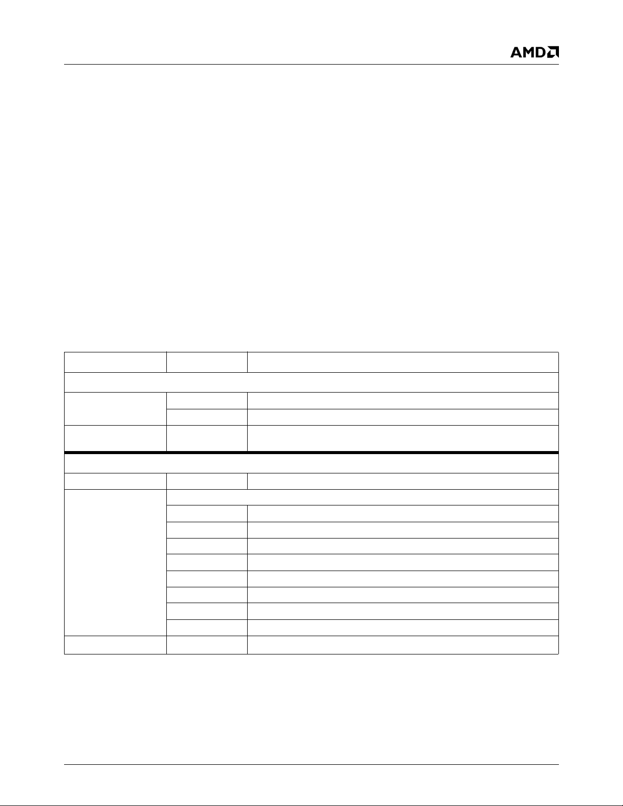
5.1.5 Mode E: SUSP#/SUSPA# with Some PCI
Clocks Stopped (Using the PM PAL)
Mode E is similar to Mode D (i.e., SUSP#/SUSPA) except
the clocks to the PCI slots and the National Semiconductor
DP83815 MacPHYTER are stopped. The PAL asser ts the
signal clocks to the clock generator to stop some PCI
clocks when: SUSPA# is low, PCIRST# is high, SUSP_3V
is high, audio is inactive, USB is inactiv e , INTR is low, SMI#
is high, and wakeup events are inactive. If USB is enabled,
the SUSPA# signal is deasser ted every 1 ms due to the 1
ms REQ1# signal from the CS5530A (USB controller).
• Mode E device status:
— GX1: Suspend
— CS5530A: Suspend
— Main memory: Active
— PCI slots: Clocks stopped
— DP83815: Inactive
— Other devices: Active
• Mode E entry event:
— Expiration of the GP Timer 1 and PAL equation
• Mode E exit event:
— Any unmasked Interrupts (e.g., keyboard or mouse
activity).
— Any asserted SMI
—NMI
— PME# from DP83815
— PME# from PCI slots
— Accessing the video port
— Video activity (any access to the VGA regis ter space,
the VGA frame buff er, the graphic accelerator control
register and the configured graphic frame buffer)
• See Section 5.1.10 "CS5530A Companion Device
Issues" on page 27 for information on interrupt wakeups.
Table 5-4 provides the required register programming for
Mode E.
Table 5-4. Mode E Register Programming
Register Setting Description
GX1 Processor
Index C2h (CCR2) Bit 7 = 1 Suspend Pins (SUSP# and SUSPA#) (1 = Enable)
Bit 3 = X Suspend-on-Halt −−> Don’t care
GX_BASE+Memory
Offset 8508h
Bit 0 = 0 Clock Stop (0 = Suspend Refresh Mode): Core stopped, the clocks to the
memory and display controller remain active
CS5530A Companion Device
F0 Index 80h Bit 0 = 1 Global Power Management (1 = Enable)
F0 Index 81h Idle Timer Enable
Bit 7 = 0 Video access (0 = Disable)
Bit 6 = 0 UDEF3 (0 = Disable)
Bit 5 = 0 UDEF2 (0 = Disable)
Bit 4 = 0 UDEF1 (0 = Disable)
Bit 3 = 0 Keyboard/Mouse (0 = Disable)
Bit 2 = 0 Parallel/Serial (0 = Disable)
Bit 1 = 0 Floppy (0 = Disable)
Bit 0 = 0 Primary HDD (0 = Disable)
F0 Index 88h
See Footnote
1
GP Timer 1 Count
AMD Geode™ GX1 Processor/CS5530A Companion Device Power Management Implementations 17
Page 18
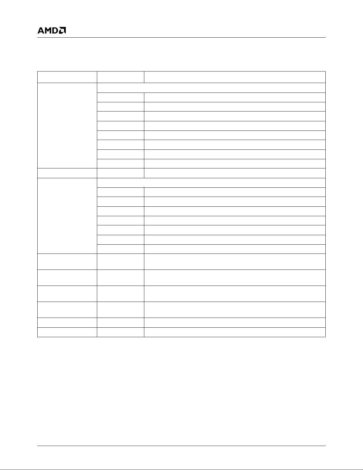
Table 5-4. Mode E Register Programming (Continued)
Register Setting Description
F0 Index 89h GPT1 Control
Bit 7 = 1 Timebase (1 = 1 sec)
Bit 6 = 0 Re-trigger on UDEF3 (0 = Disable)
Bit 5 = 0 Re-trigger on UDEF2 (0 = Disable)
Bit 4 = 0 Re-trigger on UDEF1 (0 = Disable)
Bit 3 = 1 Re-trigger on Keyboard/Mouse (1 = Enable)
Bit 2 = 1 Re-trigger on Parallel/Serial (1 = Enable)
Bit 1 = 1 Re-trigger on Floppy (1 = Enable)
Bit 0 = 1 Re-trigger on Primary HDD (1 = Enable)
F0 Index 8Ah 00h GP Timer 2 Count
F0 Index 8Bh GPT2 Control
Bit 7 = 0 Re-trigger on Secondary HDD (0 = Disable)
Bit 6 = 0 VGA Timer Base (0 = 1 ms)
Bit 5 = 0 GPT2 shift (0 = No shift)
Bit 4 = 0 GPT1 shift (0 = No shift)
Bit 3 = 1 Timebase for GPT2 (1 = 1 ms)
Bit 2 = 0 Re-trigger on GPT2 (0 = Disable)
Bits [1:0] = 00 Reserved
F0 Index 8Ch See Description
Column
F0 Index 8Dh See Description
Column
F0 Index 94h See Description
Column
F0 Index 95h See Description
Column
F0 Index AEh Any Value S/W CPU Suspend Command
F0 Index BCh Bit 0 = 0 CPU Clock Stop (0 = Normal operation)
IRQ Speedup Timer Count (timer load value): 1 ms,
a typical value = 2 to 4 ms
Video Speedup Timer Count (timer load value): 1 ms,
a typical value = 2 to 4 ms
Suspend Signal Deasserted Count (8-bit counter): 32 µs
Suspend Signal Asserted Count (8-bit counter): 32 µs
Application Note
Revision 1.0 - April 2001 - Confidential
1. The values for GPT1 and GPT2 are selected by the system designer. This value should be the maximum length of time
(in either seconds or milliseconds, depending on the counter’s timebase) that any device in the re-trigger list may remain
inactive before a power management state is triggered.
18 AMD Geode™ GX1 Processor/CS5530A Companion Device Power Management Implementations
Page 19
Application Note
Revision 1.0 - April 2001 - Confidential
5.1.6 Mode F: SUSP#/SUSPA# with GX1
Processor SUSP3V Register Set
This mode is the same as SUSP#/SUSPA# except all internal clocks of the GX1 are stopped (set GX_BASE+Memory
Offset 8508h[0] = 1). If USB is enabled, the SUSPA# signal
is deasserted every 1 ms due to the 1 ms REQ1# signal
from the CS5530A (USB controller).
• Mode F device status:
— GX1: Standby
— CS5530A: Suspend
— Main memory: Self refresh
— Other devices: Active
• Mode F entry event:
— Expiration of CS5530A GP Timer 1
• Mode F exit ev ent:
— Any unmasked interrupts (e.g., keyboard or mouse
activity)
— Any asserted SMI
—NMI
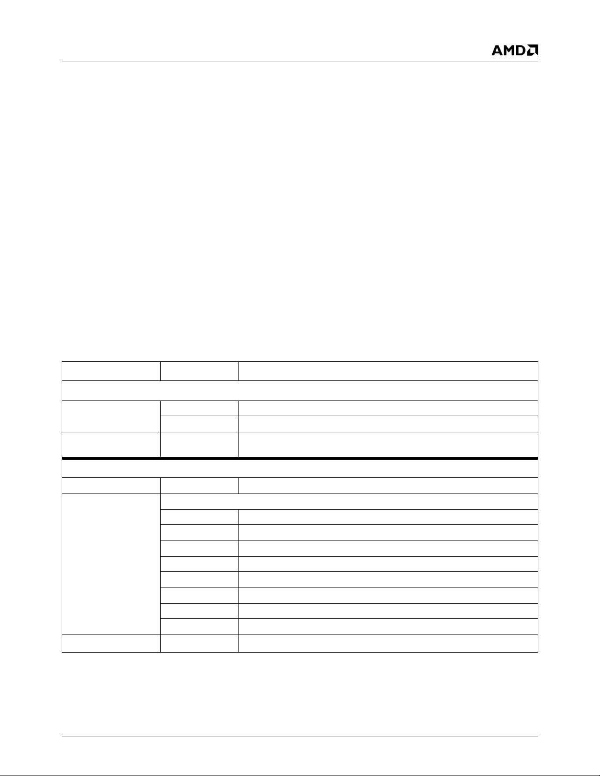
Ta ble 5-5. Mode F Register Programming
Register Setting Description
GX1 Processor
— PME# from DP83815
— PME# from PCI slots
— Accessing the video port
— Video activity (any access to the VGA regis ter space,
the VGA frame buff er, the graphic accelerator control
register and the configured graphic frame buffer)
Table 5-5 provides the required register programming for
Mode F.
5.1.6.1 Mode F: SP4GX10 Required Circuit Modification
A hardware modification is required to allow the CS5530A
to come out of 3 Volt Suspend:
• A 32.726 KHz OSC must be connected to the 32K input
pin (AE3) of CS5530A. Set register F0 Index 44h[5:4] =
10 (CLK_32K is an input) and tie the oscillator power to
.
V
CC3V
Index C2h (CCR2) Bit 7 = 1 Suspend Pins (SUSP# and SUSPA#) (1 = Enable)
Bit 3 = X Suspend-on-Halt −−> Don’t care
GX_BASE+Memory
Bit 0 = 1 Clock Stop (1 = 3 Volt Suspend Mode): The external clock may be stopped
Offset 8508h
CS5530A Companion Device
F0 Index 80h Bit 0 = 1 Global Power Management (1 = Enable)
F0 Index 81h Idle Timer Enable
Bit 7 = 0 Video access (0 = Disable)
Bit 6 = 0 UDEF3 (0 = Disable)
Bit 5 = 0 UDEF2 (0 = Disable)
Bit 4 = 0 UDEF1 (0 = Disable)
Bit 3 = 0 Keyboard/Mouse (0 = Disable)
Bit 2 = 0 Parallel/Serial (0 = Disable)
Bit 1 = 0 Floppy (0 = Disable)
Bit 0 = 0 Primary HDD (0 = Disable)
F0 Index 88h
See Footnote
1
GP Timer 1 Count
AMD Geode™ GX1 Processor/CS5530A Companion Device Power Management Implementations 19
Page 20
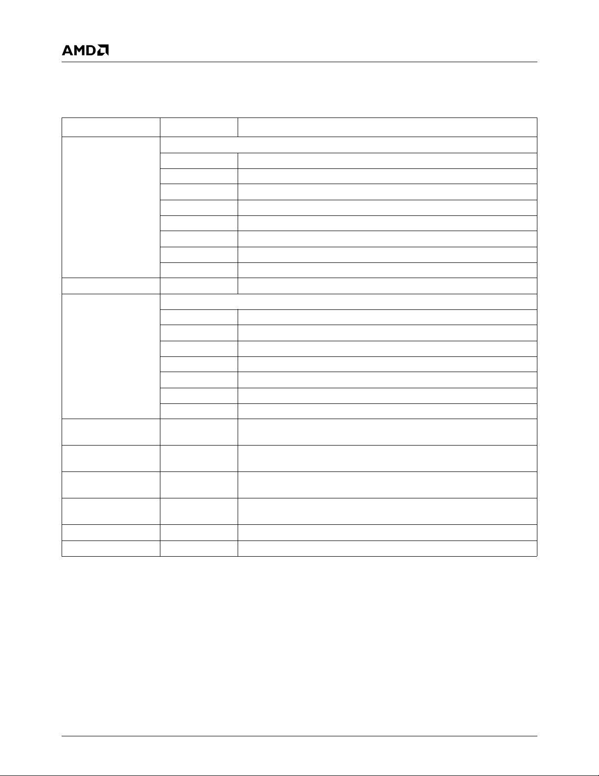
Table 5-5. Mode F Register Programming (Continued)
Register Setting Description
F0 Index 89h GPT1 Control
Bit 7 = 1 Timebase (1 = 1 sec)
Bit 6 = 0 Re-trigger on UDEF3 (0 = Disable)
Bit 5 = 0 Re-trigger on UDEF2 (0 = Disable)
Bit 4 = 0 Re-trigger on UDEF1 (0 = Disable)
Bit 3 = 1 Re-trigger on Keyboard/Mouse (1 = Enable)
Bit 2 = 1 Re-trigger on Parallel/Serial (1 = Enable)
Bit 1 = 1 Re-trigger on Floppy (1= Enable)
Bit 0 = 1 Re-trigger on Primary HDD (1 = Enable)
F0 Index 8Ah 00h GP Timer 2 Count
F0 Index 8Bh GPT2 Control
Bit 7 = 0 Re-trigger on Secondary HDD (0 = Disable)
Bit 6 = 0 VGA Timer Base (0 = 1 ms)
Bit 5 = 0 GPT2 shift (0 = No shift)
Bit 4 = 0 GPT1 shift (0 = No shift)
Bit 3 = 1 Timebase for GPT2 (1 = 1 ms)
Bit 2 = 0 Re-trigger on GPT2 (0 = Disable)
Bits [1:0] = 00 Reserved
F0 Index 8Ch See Description
Column
F0 Index 8Dh See Description
Column
F0 Index 94h See Description
Column
F0 Index 95h See Description
Column
F0 Index AEh Any Value S/W CPU Suspend Command
F0 Index BCh Bit 0 = 0 CPU Clock Stop (0 = Normal operation)
IRQ Speedup Timer Count (timer load value): 1 ms,
a typical value = 2 to 4 ms
Video Speedup Timer Count (timer load value): 1 ms,
a typical value = 2 to 4 ms
Suspend Signal Deasserted Count (8-bit counter): 32 µs
Suspend Signal Asserted Count (8-bit counter): 32 µs
Application Note
Revision 1.0 - April 2001 - Confidential
1. The values for GPT1 and GPT2 are selected by the system designer. This value should be the maximum length of time
(in either seconds or milliseconds, depending on the counter’s timebase) that any device in the re-trigger list may remain
inactive before a power management state is triggered.
20 AMD Geode™ GX1 Processor/CS5530A Companion Device Power Management Implementations
Page 21
Application Note
Revision 1.0 - April 2001 - Confidential
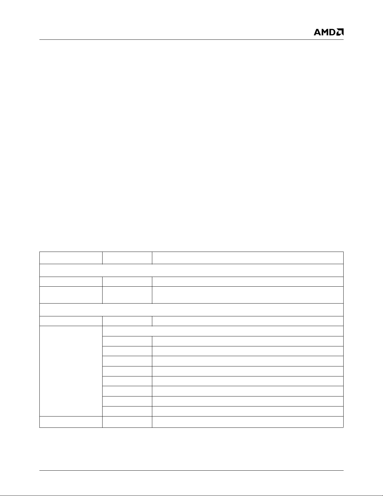
5.1.7 Mode G: SUSP#/SUSPA# and SUSP_3V
Active with All Clocks Running
The CS5530A asserts th e SUSP# signal to the GX1. The
GX1 responds by asserting the SUSPA# signal indicating
that the processor has entered Suspend. The CS5530A
asserts SUSP_3V after it has gone through the
SUSP#/SUSPA# handshake. In Mode G, by hardware
design, the SUSP_3V signal does not cause the clocks to
inhibit; all clocks are still running. The CS5530A monitors
the activity to exit from this mode.
• Mode G device status:
— GX1: Standby
— CS5530A: 3 Volt Suspend
— Main memory: Self refresh
— Other devices: Active
• Mode G entry event:
— CS5530A GP Timer 1 expiration
— Sleep button is activated (located on system board)
• Mode G exit event:
— Any unmasked interrupts (e.g., keyboard or mouse
activity)
— Any asserted SMI
Ta ble 5-6. Mode G Register Programming
—NMI
— PME# from DP83815
— PME# from PCI slots
— Accessing the video port
— Video activity (any access to the VGA regis ter space,
the VGA frame buff er, the graphic accelerator control
register and the configured graphic frame buffer)
Table 5-6 provides the required register programming for
Mode G.
5.1.7.1 Mode G: SP4GX10 Required
Circuit Modification
A hardware modification is required to allow the CS5530A
to come out of 3 Volt Suspend. An additional modification is
required for clock stopping:
• A 32.726 KHz OSC must be connected to the 32K input
pin (AE3) of CS5530A. Set register F0 Index 44h[5:4] =
10 (CLK_32K is an input) and tie the oscillator power to
.
V
CC3V
• Remove R240 from the board and remove a jumper
from J57.
Register Setting Description
GX1 Processor
Index C2h (CCR2) Bit 7 = 1 Suspend Pins (SUSP# and SUSPA#) (1 = Enable)
GX_BASE+Memory
Bit 0 = 1 Clock Stop (1 = 3 Volt Suspend Mode): The external clock may be stopped
Offset 8508h
CS5530A Companion Device
F0 Index 80h Bit 0 = 1 Global Power Management (1 = Enable)
F0 Index 81h Idle Timer Enable
Bit 7 = 0 Video access (0 = Disable)
Bit 6 = 0 UDEF3 (0 = Disable)
Bit 5 = 0 UDEF2 (0 = Disable)
Bit 4 = 0 UDEF1 (0 = Disable)
Bit 3 = 0 Keyboard/Mouse (0 = Disable)
Bit 2 = 0 Parallel/Serial (0 = Disable)
Bit 1 = 0 Floppy (0 = Disable)
Bit 0 = 0 Primary HDD (0 = Disable)
F0 Index 88h
See Footnote
1
GP Timer 1 Count
AMD Geode™ GX1 Processor/CS5530A Companion Device Power Management Implementations 21
Page 22
Application Note
Revision 1.0 - April 2001 - Confidential
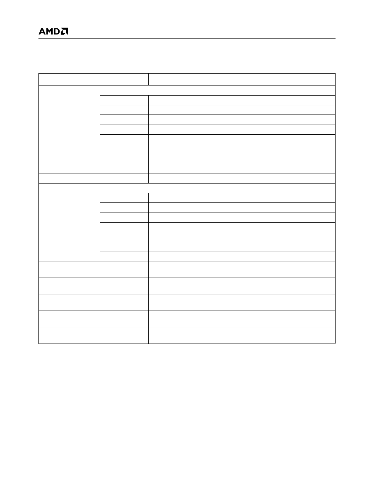
Table 5-6. Mode G Register Programming (Continued)
Register Setting Description
F0 Index 89h GPT1 Control
Bit 7 = 1 Timebase (1 = 1 sec)
Bit 6 = 0 Re-trigger on UDEF3 (0 = Disable)
Bit 5 = 0 Re-trigger on UDEF2 (0 = Disable)
Bit 4 = 0 Re-trigger on UDEF1 (0 = Disable)
Bit 3 = 1 Re-trigger on Keyboard/Mouse (0 = Enable)
Bit 2 = 0 Re-trigger on Parallel/Serial (1 = Enable)
Bit 1 = 0 Re-trigger Floppy (0 = Disable)
Bit 0 = 0 Primary HDD (0 = Disable)
F0 Index 8Ah 00h GP Timer 2 Count
F0 Index 8Bh GPT2 Control
Bit 7 = 0 Re-trigger on Secondary HDD (0 = Disable)
Bit 6 = 0 VGA Timer Base (0 = 1 ms)
Bit 5 = 0 GPT2 shift (0 = No shift)
Bit 4 = 0 GPT1 shift (0 = No shift)
Bit 3 = 1 Timebase for GPT2 (1 = 1 ms)
Bit 2 = 0 Re-trigger on GPT2 (0 = Disable)
Bits [1:0] = 00 Reserved
F0 Index 8Ch See Description
Column
F0 Index 8Dh See Description
Column
F0 Index 94h See Description
Column
F0 Index 95h See Description
Column
F0 Index AFh or
Any Value Suspend Notebook Command or
F0 Index AEh
1. The values for GPT1 and GPT2 are selected by the system designer. This value should be the maximum length of time
(in either seconds or milliseconds, depending on the counter’s timebase) that any device in the re-trigger list may remain
inactive before a power management state is triggered.
IRQ Speedup Timer Count (timer load value): 1 ms,
a typical value = 2 to 4 ms
Video Speedup Timer Count (timer load value): 1 ms,
a typical value = 2 to 4 ms
Suspend Signal Deasserted Count (8-bit counter): 32 µs
Suspend Signal Asserted Count (8-bit counter): 32 µs
S/W CPU Suspend Command
22 AMD Geode™ GX1 Processor/CS5530A Companion Device Power Management Implementations
Page 23
Application Note
Revision 1.0 - April 2001 - Confidential
5.1.8 Mode H: SUSP#/SUSPA# and SUSP3V#
Active with Some PCI Clocks Stopped
This mode is similar to Mode G, with the additional feature
that the SUSP_3V signal, asserted by CS5530A, is used to
stop some PCI clocks. The SUSP3V# signal is connected
to the “P_DOWN#” input of the clock generator.
• Mode H device status:
— GX1: Suspend
— CS5530A: 3 Volt Suspend
— Main memory: Self refresh
— PCI slots: Clocks stopped
— DP83815: Inactive
— Other devices: Active
• Mode H entry event:
— CS5530A GP Timer 1 expiration
— Sleep button is activated (located on system board)
• Mode H exit event:
— Unmasked Interrupts from IRQ1, IRQ3, IRQ4.
— Any SMI events
— PME# from DP83815
— PME# from PCI slots
• See Section 5.1.10 "CS5530A Companion Device
Issues" on page 27 for information on interrupt wakeups.
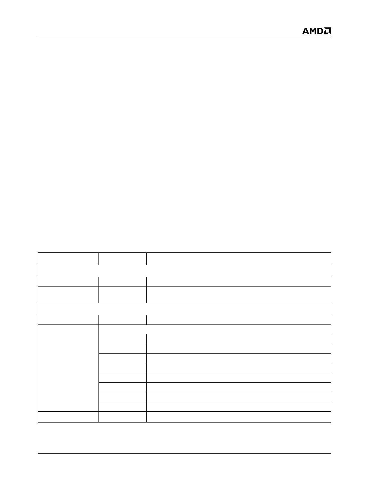
Table 5-7 provides the required register programming for
Mode H.
5.1.8.1 Mode H: SP4GX10 Required Circuit Modification
A hardware modification is required to allow the CS5530A
to come out of 3 Volt Suspend. Additional modifications are
required for clock stopping:
• A 32.726 KHz OSC must be connected to the 32K input
pin (AE3) of CS5530A. Set register F0 Index 44h[5:4] =
10 (CLK_32K is an input) and tie the oscillator power to
.
V
CC3V
• With the clock to the CPU running (KMCLKPEN default
setting):
— Remove R240 from the board.
— Omit jumper from J57.
— Wire pin 1 of R240 and pin 2 of J57.
• With the PCI clock to devices to stopped:
— Populate 10K resistor on R232. MK1491 will not have
any PCIF pins.
— Remove R240 from the board.
— Omit jumper from J57.
— Wire pin 1 of R240 and pin 2 of J57
Table 5-7. Mode H Register Programming
Register Setting Description
GX1 Processor
Index C2h (CCR2) Bit 7 = 1 Suspend Pins (SUSP# and SUSPA#) (1 = Enable)
GX_BASE+Memory
Offset 8508h
CS5530A Companion Device
F0 Index 80h Bit 0 = 1 Global Power Management (1 = Enable)
F0 Index 81h Idle Timer Enable
F0 Index 88h
Bit 0 =1 Clock Stop (1 = 3 Volt Suspend Mode): The external clock ma y be stopped
Bit 7 = 0 Video Access (0 = Disable)
Bit 6 = 0 UDEF3 (0 = Disable)
Bit 5 = 0 UDEF2 (0 = Disable)
Bit 4 = 0 UDEF1 (0 = Disable)
Bit 3 = 0 Keyboard/Mouse (0 = Disable)
Bit 2 = 0 Parallel/Serial (0 = Disable)
Bit 1 = 0 Floppy (0 = Disable)
Bit 0 = 0 Primary HDD (0 = Disable)
1
See Footnote
GP Timer 1 Count
AMD Geode™ GX1 Processor/CS5530A Companion Device Power Management Implementations 23
Page 24
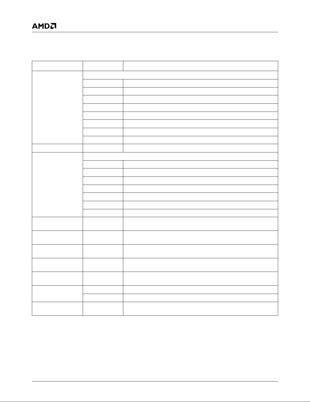
Table 5-7. Mode H Register Programming
Register Setting Description
F0 Index 89h GPT1 Control
Bit 7 = 1 Timebase (1 = 1 sec)
Bit 6 = 0 Re-trigger on UDEF3 (0 = Disable)
Bit 5 = 0 Re-trigger on UDEF2 (0 = Disable)
Bit 4 = 0 Re-trigger on UDEF1 (0 = Disable)
Bit 3 = 1 Re-trigger on Keyboard/Mouse (0 = Enable)
Bit 2 = 0 Re-trigger on Parallel/Serial (1 = Enable)
Bit 1 = 0 Re-trigger Floppy (0 = Disable)
Bit 0 = 0 Primary HDD (0 = Disable)
F0 Index 8Ah 00h GP Timer 2 Count
F0 Index 8Bh GPT2 Control
Bit 7 = 0 Re-trigger on Secondary HDD (0 = Disable)
Bit 6 = 0 VGA Timer Base (0 = 1 ms)
Bit 5 = 0 GPT2 shift (0 = No shift)
Bit 4 = 0 GPT1 shift (0 = No shift)
Bit 3 = 1 Timebase for GPT2 (1 = 1 ms)
Bit 2 = 0 Re-trigger on GPT2 (0 = Disable)
Bits [1:0] = 00 Reserved
F0 Index 8Ch See Description
Column
F0 Index 8Dh See Description
Column
F0 Index 94h See Description
Column
F0 Index 95h See Description
Column
F0 Index AEh or
Any Value S/W CPU Suspend Command or
F0 Index AFh
F0 Index BCh Bits [7:4] = 1111 PLL Delay (1111 = 15 ms)
Bit 0 =1 CPU Clock Stop (1 = Full system Suspend)
F4BAR+Memory
Bit 11 = 0 DOT Clock PLL Disable
Offset 24h
IRQ Speedup Timer Count (timer load value): 1 ms,
a typical value = 2 to 4 ms
Video Speedup Timer Count (timer load value): 1 ms,
a typical value = 2 to 4 ms
Suspend Signal Deasserted Count (8-bit counter): 32 µs
Suspend Signal Asserted Count (8-bit counter): 32 µs
Suspend Notebook Command
Application Note
Revision 1.0 - April 2001 - Confidential
1. The values for GPT1 and GPT2 are selected by the system designer. This value should be the maximum length of time
(in either seconds or milliseconds, depending on the counter’s timebase) that any device in the re-trigger list may remain
inactive before a power management state is triggered.
24 AMD Geode™ GX1 Processor/CS5530A Companion Device Power Management Implementations
Page 25
Application Note
Revision 1.0 - April 2001 - Confidential
5.1.9 Mode I: SUSP#/SUSPA# and SUSP3V#
Active with All Clocks Stopped
This state causes the GX1/CS5530A to go into the 3V Suspend mode. The SUS_3V pin from the CS5530A is tied to
the inhibit input of the clock generator. All GX1 internal
clocks as well as the external PLL are stopped. All other
system clocks are also stopped. Howeve r, power remains
applied to the GX1 and all other devices.The external 32
KHz clock for CS5530A continues to oscillate. Any SMI
event or unmasked interrupt causes the CS5530A to deassert the SUSP_3V pin, restarting the system clock.
• Mode I device status:
— GX1: Suspend
— CS5530A: 3 Volt Suspend
— Clock generator: Inhibited
— Main memory: Self refresh
— Other devices: Inactive
• Mode I entry event
— CS5530A GP Timer 1 expiration
— Sleep button is activated (located on system board)
• Mode I exit event
— Unmasked Interrupts out of IRQ1, IRQ3, IRQ4
— Any SMI events
— PME# from DP83815
— PME# from PCI slots
• See Section 5.1.10 "CS5530A Companion Device
Issues" on page 27 for information on interrupt wakeups.
5.1.9.1 Mode I: SP4GX10 Required Circuit Modification
A hardware modification is required to allow the CS5530A
to come out of 3 Volt Suspend:
• A 32.726 KHz OSC must be connected to the 32K input
pin (AE3) of CS5530A. Set register F0 Index 44h[5:4] =
10 (CLK_32K is an input) and tie the oscillator power to
.
V
CC3V
5.1.9.2 Mode I: SP4GX10 Required
Software Modifications
• Even if all clocks are stopped, the DOT clock from the
CS5530A is still running (14.318 MHz frequency). To
stop this output clock, the BIOS should disable the PLL
inside of CS5530A (F4BAR+Memory Offset 24h[11] = 0)
before going to 3 V olt Suspend and enab le it right after a
normal mode.
• The CS5530A logic that causes wakeup is combinatorial
and looks for a level high, not an edge, so the software
or BIOS needs to setup the SuperI/O to arm IRQ3 and
IRQ4 if they are unmasked and used as wakeup events.
Here is the example code for IRQ4 (COM1).
– UART enable
– Set the baud rate control register
– Out 0x3F9,0x0F; IER set
– Out 0x3FC,0x08; INT enable bit set of MCR
In al,0x3FA; Read IIR to clear possible pending
IRQ sources
– In al,0x3FE; read MSR to clear possible pending
IRQ sources
– In al,0x3FD; read LSR to clear possible pending
IRQ sources
– IRQ line should be low until something happens to
cause IRQ
Table 5-8. Mode I Required Register Programming
Register Setting Description
GX1 Processor
Index C2h (CCR2) Bit 7 = 1 Suspend Pins (SUSP# and SUSPA#) (1 = Enable)
GX_BASE+Memory
Offset 8508h
CS5530A Companion Device
F0 Index 44h Bits [5:4] = 10 CLK_32K is an input
F0 Index 80h Bit 0 = 1 Global Power Management (1 = Enable)
AMD Geode™ GX1 Processor/CS5530A Companion Device Power Management Implementations 25
Bit 0 =1 Clock Stop (1 = 3 Volt Suspend Mode): The external clock ma y be stopped
Page 26
Table 5-8. Mode I Required Register Programming (Continued)
Register Setting Description
F0 Index 81h Idle Timer Enable
Bit 7 = 0 Video access (0 = Disable)
Bit 6 = 0 UDEF3 (0 = Disable)
Bit 5 = 0 UDEF2 (0 = Disable)
Bit 4 = 0 UDEF1 (0 = Disable)
Bit 3 = 0 Keyboard/Mouse (0 = Disable)
Bit 2 = 0 Parallel/Serial (0 = Disable)
Bit 1 = 0 Floppy (0 = Disable)
Bit 0 = 0 Primary HDD (0 = Disable)
F0 Index 88h
See Footnote
F0 Index 89h GPT1 Control
Bit 7 = 1 Timebase (1 = 1 sec)
Bit 6 = 0 Re-trigger on UDEF3 (0 = Disable)
Bit 5 = 0 Re-trigger on UDEF2 (0 = Disable)
Bit 4 = 0 Re-trigger on UDEF1 (0 = Disable)
Bit 3 = 1 Re-trigger on Keyboard/Mouse (1 = Enable)
Bit 2 = 1 Re-trigger on Parallel/Serial (1 = Enable)
Bit 1 = 1 Re-trigger on Floppy (1 = Enable)
Bit 0 = 1 Re-trigger on Primary HDD (1 = Enable)
F0 Index 8Ah 00h GP Timer 2 Count
F0 Index 8Bh GPT2 Control
Bit 7 = 0 Re-trigger on Secondary HDD (0 = Disable)
Bit 6 = 0 VGA Timer Base (0 = 1 ms)
Bit 5 = 0 GPT2 shift (0 = No shift)
Bit 4 =0 GPT1 shift (0 = No shift)
Bit 3 = 1 Timebase for GPT2 (1 = 1 ms)
Bit 2 = 0 Re-trigger on GPT2 (0 = Disable)
Bits [1:0] = 00 Reserved
F0 Index 8Ch See Description
Column
F0 Index 8Dh See Description
Column
F0 Index 94h See Description
Column
F0 Index 95h See Description
Column
F0 Index AEh or
Any Value S/W CPU Suspend Command or Suspend Notebook Command
F0 Index AFh
1
GP Timer 1 Count
IRQ Speedup Timer Count (timer load value): 1 ms,
a typical value = 2 to 4 ms
Video Speedup Timer Count (timer load value): 1 ms,
a typical value = 2 to 4 ms
Suspend Signal Deasserted Count (8-bit counter): 32 µs
Suspend Signal Asserted Count (8-bit counter): 32 µs
Application Note
Revision 1.0 - April 2001 - Confidential
26 AMD Geode™ GX1 Processor/CS5530A Companion Device Power Management Implementations
Page 27
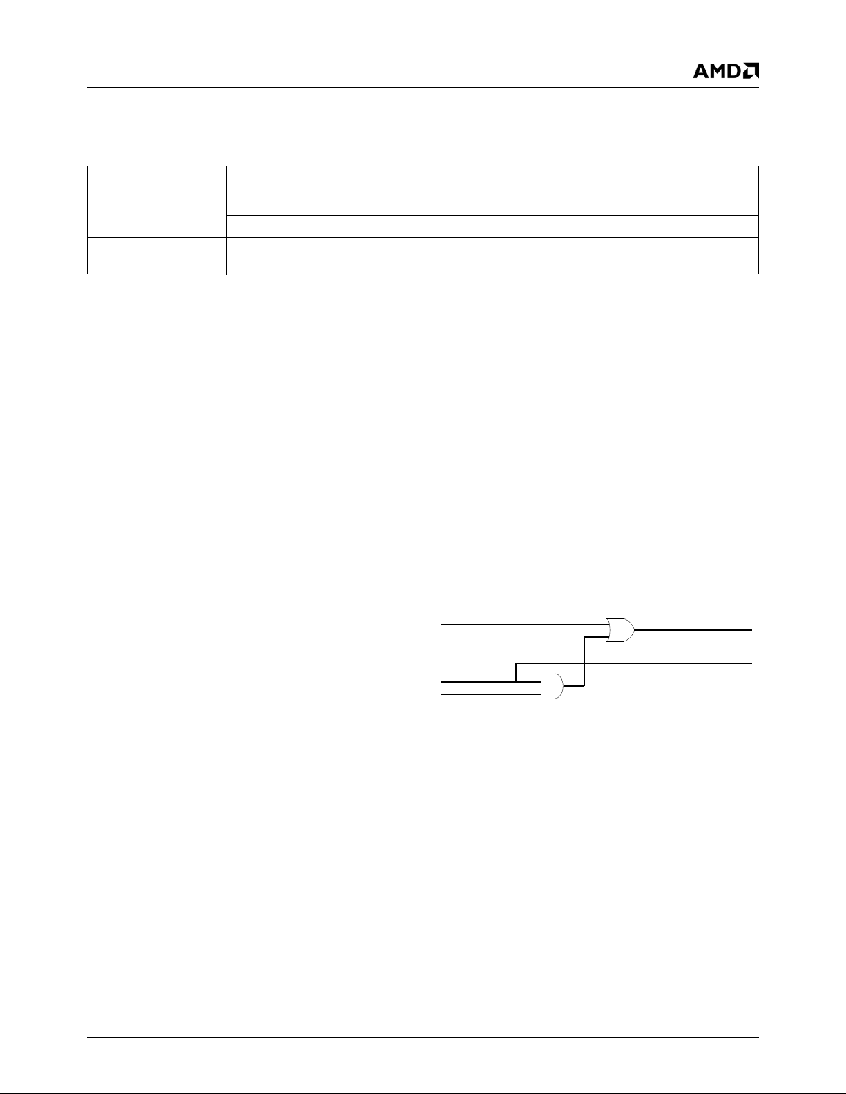
Application Note
Revision 1.0 - April 2001 - Confidential
Table 5-8. Mode I Required Register Programming (Continued)
Register Setting Description
F0 Index BCh Bits [7:4] = 1111 PLL Delay (1111 = 15 ms)
Bit 0 =1 CPU Clock Stop (1 = Full system Suspend)
F4BAR+Memory
Offset 24h
1. The values of GPT1 and GPT2 are selected by the system designer. This value should be the maximum length of time
(in either seconds or milliseconds, depending on the counter’s timebase) that any device in the re-trigger list may remain
inactive before a power management state is triggered.
Bits [11] = 0 DOT Clock PLL Disable
5.1.10 CS5530A Companion Device Issues
The following items, copied verbatim from the specification
update document are reproduced here for completeness.
These issues are referenced in Section 5.1.5 on page 17.
5.1.10.1 CS5530A, Silicon Revision B1 (Document
Revision 5.0): Issues #6 and #13
6. Some GPIO wakeup events do not w ork if the PCI
clock has been stopped in 3V Suspend
Description: The PCI clock is used to clock all
GPIOs into the part. GPIO[2:0] have a combinational
path to the SUSP_3V signal to deassert it. GPIO[7:3]
do not have this path and can not wak e the system. If
the clock is stopped, then GPIO[7:3] can not
generate a wakeup event.
Implications: GPIO[7:3] cannot be used as wakeup
events if the PCI clock is stopped.
Resolution: Do not use GPIO[7:3] as wakeup ev ents
when the PCI clock is stopped in 3V Suspend.
13. All IRQ wakeup events do not work if the PCI
clock has been stopped in 3V Suspend
Description: IRQs can not be used to wake the
system if the PCI clock has been stopped in 3V
Suspend.
Implications: If a system design uses 3V Suspe nd,
an IRQ can not be used to wake the system.
Resolution: Keep the PCI clock running if IRQs are
to be used as wakeup events. If not, a hardware
workaround will be needed to correct this problem by
connecting IRQx to GPIO2, as shown in Figure 2-2.
(Also see issue 6 on page 2.)
The circuit assumes that IRQx is a rising edge
wakeup event and that the SUSP_3V pin is active
high (clocks stop when SUSP_3V is high). With this
connection, GPIO2 will generate an SMI that the
system must handle.
Hence, if 3V Suspend is to be used in the system
design, it is recommended to assign GPIO2 as the
system wakeup with the IRQs as simply additional
wakeup sources.
GPIO2 from system
GPIO2 to CS5530A
IRQx to CS5530A
IRQx
SUSP_3V
Note: Additional inverters may be necessary if IRQx
and/or SUSP_3V have different polarity.
Figure 2-2. IRQx Wakeup Connections
AMD Geode™ GX1 Processor/CS5530A Companion Device Power Management Implementations 27
Page 28
Application Note
Revision 1.0 - April 2001 - Confidential
5.2 Mode Summary
Tables 5-9, 5-10, and 5-11 give a summar y of the clocks,
device status, and peripheral status for each of the Working
state modes. The precise details for implementing each of
these states is detailed in Section 5.1 "Mode Programming"
Table 5-9. Clock Status During Working State Modes
Clock Signal
Name Freq. Device Mode A Mode B Mode C Mode D Mode E Mode F Mode G Mode H Mode I
CLK$PCICPU33MGX1 RRRRRRRSS
CLK$PCIKAH 33M CS5530A RRRRSRRSS
CLK$PCI83815 33M DP83815 RRRRSRRSS
CLK$PCISL133MPCI Slot 1RRRRSRRSS
CLK$PCISL233MPCI Slot 2RRRRSRRSS
CLK$USB 48M CS5530A RRRRRRRRS
CLK$SUP 14M PC97317 RRRRRRRRS
CLK$AUDAC9725MAC97 RRRRRRRRS
CLK$KAH14M 14M CS5530A RRRRRRRRS
CLK$ISAOSC14MISA SlotsRRRRRRRRS
32KHz 32K CS5530A RRRRRRRRR
ETC
SDCLOCKs
Out of GX1
VID_CLK
Out of GX1
PCLK
Out of GX1
DCLK
Out of CS5530A
CLK$ISA
Out of CS5530A
Note: R = Running; S = Stopped.
1. Depends upon graphics mode.
66M~
Main
80M
Memory
1
CS5530A RRRRR R SSS
1
CS5530A RRRRR R SSS
1
GX1 RRRRR R SSS
TBD ISA
Device
RRRRR SR SS
RRRRS R R SS
starting on page 12. Each mode has a detailed description
of entry and exit events, as w ell as a dedicated register programming table that shows how to set up the Geode
devices to support the mode being discussed.
28 AMD Geode™ GX1 Processor/CS5530A Companion Device Power Management Implementations
Page 29
Application Note
Revision 1.0 - April 2001 - Confidential
Table 5-10. Device Status During Worki ng State Modes
Device Mode A Mode B Mode C Mode D Mode E Mode F Mode G Mode H Mode I
GX1
(Processor)
CS5530A
(Companion)
MK1491 (Clock
Generator)
Main Memory Active Active Active Active Active Self
PCI Slots Active Active Active Active Inactive Active Active Inactive Inactive
DP83815
(Ethernet Controller)
PC97317
(SuperI/O)
AC97 (Audio
Codec)
DS90C381
(LVDS)
ISA Slots Active Active Active Active Active Active Active Active Inactive
1. Definitions of the terms and states used in this table are in Section 6.4 "Device and Peripheral Power States" on page 33.
Active Suspend
Modulation
Active Suspend
Modulation
Active Active Active Active Active Active Active PCI_STOP Inhibited
Active Active Active Active Inactive Active Active Inactive Inactive
Active Active Active Active Active Active Active Active Inactive
Active Active Active Active Active Active Active Active Inactive
Active Active Active Active Active Active Active Active Inactive
Active Idle Suspend Suspend Suspend Suspend Suspend 3 Volt
Active Idle Suspend Suspend Suspend Suspend Suspend 3 Volt
Refresh
1
Self
Refresh
Self
Refresh
Suspend
Suspend
Self
Refresh
Table 5-11. Peripheral Status During Working State Modes
Device Mode A Mode B Mode C Mode D Mode E Mode F Mode G Mode H Mode I
External
Monitor
TFT LCD
Panel
DSTN LCD
Panel
HDD Active Active Active Active Active Active Inactive Inactive Inactive
CD-ROM Active Active Active Active Active Active Inactive Inactive Inactive
FDD Active Active Active Active Active Active Inactive Inactive Inactive
1. Definitions of the terms and states used in this table are in Section 6.4 "Device and Peripheral Power States" on page 33.
Active Active Active Inactive Inactive Inactive Inactive Inactive Inactive
Active Active Active Inactive Inactive Inactive Inactive Inactive Inactive
Active Active Active Inactive Inactive Inactive Inactive Inactive Inactive
1
AMD Geode™ GX1 Processor/CS5530A Companion Device Power Management Implementations 29
Page 30

6.0 Peripheral Power Management
The CS5530A provides peripheral power management
using a combination of device idle timers, address traps,
and general purpose I/O pins. Idle timers are used in conjunction with traps to support powering down peripheral
devices. Eight programmable GPIO (general purpose I/O)
pins are included for external device power control as well
as other functions. All I/O addresses are decoded in 16
bits. All memory addresses are decoded in 32 bits.
Peripheral power management is handled independently of
system power management by means of the device idle
timers and traps.
6.1 Device Idle Timers and Traps
Idle timers are used to power manage a peripheral by
determining when the peripheral has been inactive for a
specified period of time, and removing power from the
peripheral at the end of that time period.
Idle timers are provided by the CS5530A for the commonlyused peripherals (FDC, IDE, parallel/serial ports, and
mouse/keyboard). In addition, there are three user-defined
timers that can be configured for either I/O or memory
ranges. The Power Management enable bit (F0 Index
80h[1]) enables and disables the power management idle
timers. The Trap bit in the sa me register (F0 Index 80h[2])
enables and disables device I/O traps.
The idle timers are 16-bit countdown timers with a 1 second timebase, providing a time-out range of 1 to 65536
seconds (1092 minutes) (18 hours). General purpose timers can be programmed to count milliseconds instead of
seconds.
When the idle timers are enabled, the timers are loaded
from the timer count registers and start to decrement at the
next timebase clock, but cannot trigger an interrupt on that
cycle. If an idle timer is initially set to 1, it decrements to 0
on the first cycle and continues counting with 65535 on the
next cycle. Starting at 2 gives 1 on the first cycle, and 0 on
the second cycle, generating the interrupt. Since the timebase is one second, the minimum interval before the next
interrupt from this timer is variable, from one to two seconds with a setting of two.
The idle timers continue to independently decrement until
one of two possibilities occurs: a bus cycle occurs at that
I/O or memory range, or the timer decrements to zero.
When a bus cycle occurs, the idle timer is reloaded with its
starting value. It then resumes decrementing from the new
value.
When the timer decrements to zero, if power management
is enabled (F0 Index 80h[0] = 1), the timer generates an
SMI. (F0 Index 80h[0] = 0 does not disable these timers
from running, but only from generating an SMI.)
Application Note
Revision 1.0 - April 2001 - Confidential
When an idle timer generates an SMI, the SMI handler
manages the peripheral power, disables the timer, and
enables the trap. The next time an event occurs, the trap
generates an SMI. This time, the SMI handler applies
power to the peripheral, enables the timer (thus reloading
its starting value), and disables the trap.
Tables 8-11 (star ting on page 50) through 8-19 sh ow the
device associated idle timers’ and traps’ programming bits.
Although not considered as device idle timers, two additional timers are provided by the CS5530A. The Video Idle
Timer used for Suspend determination and the VGA Timer
used for SoftVGA. These timers and their associated programming bits are listed in Tables 8-20 and 8-21.
6.2 General Purpose Timers
The CS5530A contains two general purpose timers, General Purpose Timer 1 (F0 Index 88h) and General Purpose
Timer 2 (F0 Index 8Ah). These two timers are similar to the
Device Idle Timers in that they count down to zero unless
re-triggered, and generate an SMI when they reach zero.
However, these are 8-bit timers instead of 16 bits, they
have a programmable timebase, they are not enabled or
disabled by Global Power Management bits F0 Index
80h[1:0], and the events that reload these timers are configurable. These timers are typically used for an indication
of system inactivity for Suspend determination.
General Purpose Timer 1 can be re-tr iggered by activity to
any of the configured user defined devices, keyboard and
mouse, parallel and serial, floppy disk, or hard disk.
General Purpose Timer 2 can be re-triggered by a transition on the GPIO7 pin (if GPIO7 is properly configured).
(Refer to the CS5530A data book for GPIO programming
information.)
The timebase for both general purpose timers can be configured as either 1 second (default) or 1 millisecond. The
registers at F0 Index 89h and 8Bh are the control registers
for the general purpose timers. Table 8-11 on page 50
show the bit formats for these registers.
After a general purpose timer is e nabled or after an event
reloads the timer, the timer is loaded with the configured
count value. Upon expiration of the timer an SMI is generated and a status flag is set. Once expired, this timer must
be re-initialized by disabling and enabling it.
30 AMD Geode™ GX1 Processor/CS5530A Companion Device Power Management Implementations
Page 31

Application Note
Revision 1.0 - April 2001 - Confidential
The general purpose timer is not loade d immediately, but
when the free-running timebase counter reaches its maximum value. Depending on the count at the time, this could
be on the next 32 KHz clock (CLK_32K), or after a full
count of 32, or 32,768 clocks (approximately 1 msec, or
exactly 1 sec). The general purpose timer cannot trigger an
interrupt until after the first count. Thus, the minimum time
before the next SMI from the timer can be either from 12 msec or 1-2 sec with a setting of 02h.
6.2.1 ACPI Timer Register
The ACPI Timer Count register (F1BAR+Memory Offset
1Ch or a fixed I/O P ort at 121Ch) provides the current value
of the ACPI timer. The timer counts at 14.31818/4 MHz
(3.579545 MHz). If SMI generation is enabled (F0 Index
83h[5] = 1), an SMI is generated when bit 23 toggles.
Table 8-6 on page 43 shows the ACPI Timer Count register
and the ACPI Timer SMI enable bit.
6.2.2 V-ACPI I/O Register Space
The register space designated as V-ACPI (Virtualized
ACPI) I/O does not physically exist in the CS5530A. ACPI
is supported in the CS5530A by virtualizing this register
space. In order for ACPI to be supported, the V-ACPI module must be included in the BIOS.
Fixed Feature space registers are required to be implemented by all ACPI-compatible hardware. The Fixed Feature registers in the V-ACPI solution are mapped to normal
I/O space starting at Offset AC00h. However, the designer
can relocate this register space at compile time, hereafter
referred to as A C PI_BA SE. Re gisters w ithi n the V-ACPI I/O
space must only be accessed on their defined boundaries.
For example, BYTE aligned registers must not be
accessed via WORD I/O instructions, WORD aligned registers must not be accessed as DW OR D I/O instructions, etc.
The register descriptions provided in Table 8-7 on page 44
are for reference only. Refer to the CS5530A data book for
detailed bit descriptions.
6.3 Power Management SMI Status Reporting Registers
The CS5530A updates status registers to reflect the SMI
sources. Power management SMI sources are the device
idle timers, address traps, and general purpose I/O pins.
Power management events are repor ted to the processor
through the active low SMI# pin. When an SMI is initiated,
the SMI# pin is asserted l ow and is held low until all SMI
sources are cleared. At that time, SMI# is deasserted.
All SMI sources report to the CS5530A Top Level SMI Status Register (F1BAR+Memory Offset 02h) and the Top
Level SMI Status Mirror Register (F1BAR+Memory Offset
00h). The Top SMI Status and Status Mirror Registers are
the top level of hierarch y for the SMI handler in determining
the source of an SMI. These two registers are identical
except that reading the register at F1BAR+Memory Offset
02h clears the status.
Since all SMI sources report to the Top Level SMI Status
Register, many of its bits combine a large number of ev ents
requiring a second level of SMI status reporting. The second level of SMI status reporting is set up very much like
the top level. There are two status reporting registers, one
“read only” (mirror) and one “read to clear”. The data
returned by reading either offset is the same, the difference
between the two being that the SMI can not be cleared by
reading the mirror register.
Figure 6-1 shows an example SMI tree for checking and
clearing the source of general purpose timer and the user
defined trap generated SMIs.
Table 8-8 on page 44 shows the bit formats of the read to
clear Top Level SMI Status Register (F1BAR+Memory Offset 02h). Table 8-9 star ting on page 45 shows the bit formats of the read to clear second level SMI status registers.
For information regarding the location of the corresponding
mirror register, refer to the note in the footer of the register
description.
Keep in mind, all SMI sources in the CS5530A are reported
into the Top Level SMI Status Registers (F1BAR+Memory
Offset 00h/02h); however, this discussion is regarding
power management SMIs.
AMD Geode™ GX1 Processor/CS5530A Companion Device Power Management Implementations 31
Page 32
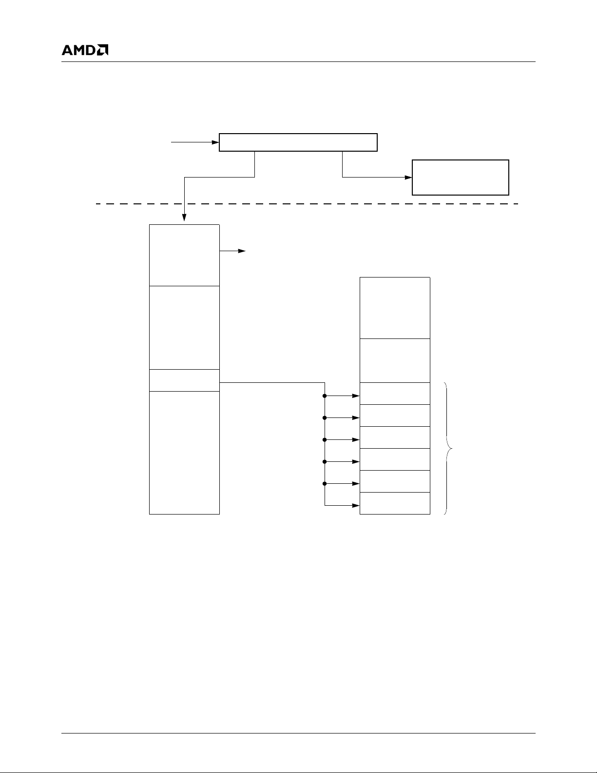
SMI# Asserted SMM software reads SMI Header
Application Note
Revision 1.0 - April 2001 - Confidential
AMD Geode™
GX1 Processor
AMD Geode™
CS5530A
Companion
Device
If Bit X = 1
(External SMI)
F1BAR+Memory
Offset 02h
Read to Clear
to determine
top-level source
of SMI
Bits [15:10]
Other_SMI
Bit 9
GTMR_TRP_SMI
Bits [8:0]
Other_SMI
Top Level Second Level
SMI Deasserted after all SMI Sources are Cleared
(i.e., Top and Second Levels - note some sources may have a Third Level)
If bit 9 = 1,
Source of SMI
is GP Timer or UDEF Trap
If Bit X = 0
(Internal SMI)
F1BAR+Memory
Offset 06h
Read to Clear
to determine
second-level
source of SMI
Bits 15:6
RSVD
Bit 5
PCI_TRP_SMI
Bit 4
UDEF3_TRP_SMI
Bit 3
UDEF2_TRP_SMI
Bit 2
UDEF1_TRP_SMI
Bit 1
GPT2_SMI
Bit 0
GPT1_SMI
Call internal SMI handler
to take appropriate action
Take
Appropriate
Action
Figure 6-1. General Purpose Timer and UDEF Trap SMI Tree Example
32 AMD Geode™ GX1 Processor/CS5530A Companion Device Power Management Implementations
Page 33

Application Note
Revision 1.0 - April 2001 - Confidential
6.4 Device and Peripheral Power States
In this section, the details of power states are defined for
each major device and peripheral on the SP4GX10. Specific designs may omit certain devices or peripherals, or
include others not described here. Note that the SP4GX10
contains or supports all the devices and peripherals
described here. These state descriptions are referred to
using their one-word titles, in Table 5-10 and Table5-11 on
page 29.
6.4.1 GX1 Processor
The GX1 processor supports a wide variety of hardware
and software controlled modes. The information summarized here is explained in much greater detail in Section 4.1
"GX1 Processor/CS5530A Companion Device Power
States" on page 3 of this application note.
• Full-On
• Suspend Modulation: Automatic throttling of CPU core.
• Suspend-On-Halt, also called Active Idle: Core stopped,
display active; the clocks to the memory and display
controller remain active.
— To support these modes, the CLK_STP bit
(GX_BASE+Memory Offset 8508h[0]) must be
cleared to 0; enabling the Suspend Refresh mode. In
Suspend Refresh mode the clocks to the memory
and display controller remain active during Suspend.
• Suspend: Core and all integrated functions halted; all
internal clocks are stopped and the external SYSCLK
input is still running.
• 3 V olt Suspend: Core and all integrated functions halted
with the external SYSCLK input stopped.
— To support this mode, the CLK_STP bit
(GX_BASE+Memory Offset 8508h[0]) must be set to
1; enabling 3 Vol t Suspend mode. In 3 Volt Suspen d
mode the external clock may be stopped.
6.4.2 CS5530A Companion Device
The CS5530A supports a wide variety of hardware and
software controlled modes. The information summarized
here is explained in much greater detail in Section 4.1
"GX1 Processor/CS5530A Companion Device Power
States" on page 3 of this application note.
• Suspend Modulation: Automatic duty-cycle control of
CPU core.
• Suspend: In this mode, all external clocks are running.
The CS5530A asserts the SUSP# signal to the GX1
processor and the processor responds by asserting the
SUSPA# signal, indicating that the processor has
entered Suspend. The CS5530A monitors the activity to
exit from this mode.
• 3 V olt Suspend: In this mode, either all or some external
clocks are stopped. The CS5530A asserts the SUSP#
signal to GX1 processor and the processor responds by
asserting the SUSPA# signal indicating that the
processor has entered Suspend. The CS5530A asserts
the SUSP3V# upon completion of the SUSP#/SUSPA#
handshake. SUSP3V# is intended to be connected to
the output enable of a clock generator so that the clock
to the GX1 processor and CS5530A will be stopped.
The CS5530A monitors the activity to exit from this
mode.
6.4.3 Main Memory
Memory can operate in two modes.
• Active: Normal operation.
• Self Refresh: The clock to the input pin is stopped. The
SDRAM disables the internal clock and all the input
buffers except CKE. The refresh addressing and timing
are internally generated to reduce power consumption.
This mode is entered when the banks are in the Idle
state by asserting low on CS#, RAS#, CAS#, and CKE
with high on WE#.
6.4.4 MK1491 Clock Generator
The ICS MicroClock MK1491 has three operational modes.
• Active: Normal operation.
• PCI_STOP: The output of PCI clocks will be low except
for the PCIF pin. The PCIF pin is determined by a
resistor option.
• Inactive: All outputs are low and the PLL and oscillator
(inside of MK1491) are off.
6.4.5 DP83815 Ethernet Controller
The National Semiconductor DP83815 MacPHYTER has
two operational modes.
• Active: Normal operation.
• Inactive: The external PCI clock is stopped and the
device is in power-down mode. However, the circuit for
Wake-on-LAN is activ e.
6.4.6 PC97317 SuperI/O
The National Semiconductor PC97317 SuperI/O has two
operational modes.
• Active: Normal operation.
• Inactive: The external 14.318 MHz clock to this device is
stopped and the device is in the power-down mode.
Howeve r, the circuit for Advanced Power Control and
RTC is active through 32 KHz and 5.0V standby.
AMD Geode™ GX1 Processor/CS5530A Companion Device Power Management Implementations 33
Page 34

Application Note
Revision 1.0 - April 2001 - Confidential
6.4.7 Audio AC97
• Active: Normal operation.
• Inactive: The external DOT clock to this device is
stopped.
6.4.8 External Monitor
• Active: Normal operation.
• Inactive: If there is no activity on the SYNC input, the
monitor will power-down.
6.4.9 TFT LCD Panel
• Active: Normal operation.
• Inactive: The display output on the panel is off, including
the backlight. Mode is controlled by the CS5530A.
6.4.10 DSTN LCD Panel
• Active: Normal operation.
• Inactive: The display output on the panel is off, including
the backlight.
6.4.11 Hard Disk Drive (HDD)
• Active: Normal operation.
• Inactive: The device interface is capable of accepting
commands. The spindle motor is stopped and all
circuitry except the host interface is in the power saving
mode. The execution of commands is delayed until the
spindle is ready .
6.4.12 CD-ROM
• Active: Normal operation.
• Inactive: The device interface is capable of accepting
commands. The spindle motor is stopped and all
circuitry except the host interface is in the power saving
mode. The execution of commands is delayed until the
spindle is ready .
6.4.13 Floppy Disk Drive (FDD)
• Active: Normal operation.
• Inactive: The device interface is capable of accepting
commands. The spindle motor is stopped and all
circuitry except the host interface is in the power saving
mode. The execution of commands is delayed until the
the spindle is ready.
34 AMD Geode™ GX1 Processor/CS5530A Companion Device Power Management Implementations
Page 35
Application Note
Revision 1.0 - April 2001 - Confidential
7.0 Power Measurements
Actual power measurements were made on an SP4GX10.
These measurements may be used to give an indication of
the relative power savings that can be realized by using the
various Working state Modes A through I presented in Section 5.0 on page 12.
7.1 Method of Measurement
The SP4GX10 has four primary power planes:
• RTC battery power plane:
— Pow er to the real-time clock and NVRAM in external
RTC. The plane is powered via “coin-cell” lithium
battery.
• Standby power plane:
— This plane will be on to control the main power plane
and wakeup event. It supplies the pow er for the
Advanced Power Control circuit inside the PC97317.
POWERON# from the PC97317 turns on the main
power plane and deasserting POWERON# (driven
high) will cut the main power. This state is ref erred as
the Off state in previous sections. The minimum
circuit to support the on and wakeup event is
powered by this plane. This plane is always powered
except during the Mechanical Off state. (Refer to
Section 4.2 "System Platform Pow er States" on page
7 for descriptions of “Off” and “Mechanical Off”
states.)
• 3 Volt Standby power plane:
— To support the Wake-on-LAN event, this plane is
powered to the DP83815 and is always powered
except during the Mechanical Off state.
• Main power plane
— Contains all the rest of the system power (5V, 3.3V,
+12V, -12V, -5V).
7.2 Measurement Results
Figure 7-1 presents a stacked-bar chart showing the contributions of each major system element to the overall power
consumption, under each Working state Mode A through I.
Each bar contains, from the top to the bottom, power measurements for the GX1, memories, clock generator, and
CS5530A. The system on which these measurements
were taken was a standard SP4GX10, with an external
video card in one of the PCI slots. No regular SMI events
were occurring during these measurements. If SMI events
were regularly occurring, the system would periodically
wakeup to service them, thus registering an increase in
power during times when the system would otherwise be in
a low-power state.
In this chart, the detailed power numbers are not of interest; the reader should instead compare the relative
changes in overall system power consumption from one
mode to the next. System designers may use this information to evaluate the potential power savings that may be
realized by implementing any of the modes described, and
may then make a decision as to whether or not implementing that mode would be of benefit to the end product.
4
3.5
3
Watts
2.5
2
1.5
1
0.5
0
ABCDEFGH I
Mode
GX1
Mem o ry
Clk Gen
CS5530A
Figure 7-1. Power Consumption For Each Working State Mode
AMD Geode™ GX1 Processor/CS5530A Companion Device Power Management Implementations 35
Page 36
8.0 Register Programming Tables
The tables in this section are provided for reference. This
information is extracted from the GX1 and CS5530A data
books (hence, table number references within these tables
refer to the table/page number in the data book). These
tables provide the details necessary for a detailed designer
to configure the Geode devices for the modes and states
selected by the system designer.
8.1 GX1 Processor Power Management Registers
Table 8-1 provides the bit formats for the Serial Packet register. Details regarding the usage of this register can be
found in Section 3.1 "GX1 Processor Serial Packet Interface" on page 2.
Table 8-1. GX1 Processor Power Management Serial Packet Register
Bit Name Description
Application Note
Revision 1.0 - April 2001 - Confidential
Table 8-2 on page 37 shows the bits related to configuring
the GX1 for Suspend mode. Usage information for these
bits can be found in:
• Index C2h: Section 4.1.3 "Suspend-on-Halt" and Section
4.1.4 "CPU Suspend" on page 3.
• Index C3h: Section 4.1.2 "System Management Mode"
and Section 4.1.4 "CPU Suspend" on page 3.
• GX_BASE+Memory Offset 8508h: Section 4.1.6 "3 Volt
Suspend" on page 5, Section 5.1.6 "Mode F:
SUSP#/SUSPA# with GX1 Processor SUSP3V Register
Set" on page 19, and Section 6.4.1 "GX1 Processor" on
page 33.
GX_BASE+Memory Offset 850Ch-850Fh PM_SER_PACK Register (R/O) Default Value = xxxxxx00h
31:8 RSVD Reserved: These bits are not used. Do not write to these bits.
7VID_IRQVideo IRQ: This bit indicates the occurrence of a video vertical sync pulse. This bit is set at the same time
that the VINT (Vertical Interrupt) bit is set in the DC_TIMING_CFG register. The VINT bit has a corresponding enable bit (VIEN) in the DC_TIM_CFG register (Table 4-29 on page 145).
6CPU_ACTCPU Activity: This bit indicates the occurrence of a level 1 cache miss that was not a result of an instruc-
tion fetch. This bit has a corresponding enable bit in the PM_CNTL_TEN register.
5:2 RSVD Reserved: Set to 0.
1USR_DEFProgrammable Address Decode: This bit indicates the occurrence of a programmable memory address
decode. This bit is set based on the values of the PM_BASE register and the PM_MASK register (see
Table 5-3 on page 184). The PM_BASE register can be initialized to any address in the full 256 MB
address range.
0VID_DECVideo Decode: This bit indicates that the CPU has accessed either the display controller registers or the
graphics memory region. This bit has a corresponding enable bit in the PM_CNTRL_TEN.
Note: The AMD Geode™ GX1 processor transmits the contents of the serial packet only when a bit in the packet register is set and
the interval counter has elapsed. The AMD Geode™ CS5530A companion device decodes the serial packet after each transmission. Once a bit in the packet is set, it will remain set until the completion of the next packet transmission. Successive
events of the same type that occur between packet transmissions are ignored. Multiple unique events between packet transmissions will accumulate in this register.
36 AMD Geode™ GX1 Processor/CS5530A Companion Device Power Management Implementations
Page 37
Application Note
Revision 1.0 - April 2001 - Confidential
Table 8-2. GX1 Processor Suspend Mode Related Bits
Bit Name Description
Index C2h CCR2: Configuration Control Register 2 (R/W) Default Value = 00h
7 USE_SUSP Enable Suspend Pins:
If = 1: SUSP# input and SUSPA# output are enabled.
If = 0: SUSP# input is ignored.
3 SUSP_HLT Suspend-on-Halt:
If = 1: CPU enters Suspend mode following execution of a HLT instruction.
Note: All bits are cleared to zero at reset.
Index C3h CCR3: Configuration Control Register 3 (R/W) Default Value = 00h
3 SUSP_SMM_EN Enable Suspend in SMM Mode:
If = 0: SUSP# ignored in SMM mode.
If = 1: SUSP# recognized in SMM mode.
Note: All bits are cleared to zero at reset.
GX_BASE+Memory Offset 8508h-850Bh PM_CNTRL_CSTP Register (R/W) Default Value = xxxxxx00h
0 CLK_STP Clock Stop: This bit configures the GX1 processor for Suspend Refresh Mode or 3 Volt Suspend
Note: When bit 0 is set high and the Suspend input pin (SUSP#) is asserted, the AMD Geode™ GX1 processor stops all it’s internal
clocks, and asserts the Suspend Acknowledge output pin (SUSPA#). Once SUSPA# is asserted the GX1 processor’s
SYSCLK input can be stopped. If bit 0 is cleared, the internal memory controller and display controller clocks are not stopped
on the SUSP#/SUSPA# sequence, and the SYSCLK input can not be stopped.
Mode:
0 = Suspend Refresh Mode. The clocks to the memory and display controller remain active during
Suspend.
1 = 3 Volt Suspend Mode. The external clock may be stopped during Suspend.
AMD Geode™ GX1 Processor/CS5530A Companion Device Power Management Implementations 37
Page 38
Revision 1.0 - April 2001 - Confidential
8.2 CS5530A Companion Device Power Management Registers
Table 8-3 shows the bits related to configuring the
CS5530a for Suspend mode. Usage information for these
bits can be found in:
• F0 Index A8h:
— No specific text reference, works in conjunction with
the Video Speedup timer (F0 Index 8Dh)
Application Note
• F0 Index 80h:
— Section 4.1.5.3 "Configuring Suspend Modulation" on
page 5
— Section 4.1.7 "Trigg ering Suspend State" on page 6
— Section 6.1 "Device Idle Timers and Traps" on page
30
— Section 6.2 "General Purpose Timers" on page 30
• F0 Index 8Ch, 8Dh, 94h, 95h:
— Section 4.1.5.3 "Configuring Suspend Modulation" on
page 5
• F0 Index 96h:
— Section 4.1.3 "Suspend-on-Halt" on page 3
— Section 4.1.5.3 "Configuring Suspend Modulation" on
page 5
• F0 Index AEh:
— Section 4.1.7 "Triggering Suspend State" on page 6
— Section 4.2.5.2 "Advanced Power Management
States" on page 10
• F0 Index BCh:
— Section 4.1.4 "CPU Suspend" on page 3
— Section 4.1.6 "3 Volt Suspend" on page 5
— Section 4.1.7 "Triggering Suspend State" on page 6
• F0 Index D0h:
— Section 4.2.5.2 "Advanced Power Management
States" on page 10
• F1BAR+Memory Offset 08h-09h:
— Section 4.1.5.4 "SMI Speedup Disable" on page 5
Table 8-3. CS5530A Suspend/Suspend Modulation Configuration Related Registers
Bit Description
F0 Index 80h Power Management Enable Register 1 (R/W) Reset Value = 00h
7:6 Reserved: Set to 0.
5 Codec SDATA_IN SMI: Allow AC97 codec to generate an SMI due to codec producing a positive edge on SDATA_IN.
0 = Disable; 1 = Enable.
Top level SMI status is reported at F1BAR+Memory Offset 00h/02h[0].
Second level SMI status is reported at F0 Index 87h/F7h[2].
4 Video Speedup: Any video activity, as decoded from the serial connection (PSERIAL register, bit 0) from the GX-series pro-
cessor disables clock throttling (via SUSP#/SUSPA# handshake) for a configurable duration when the system is power managed using CPU Suspend modulation. 0 = Disable; 1 = Enable.
The duration of the speedup is configured in the Video Speedup Timer Count Register (F0 Index 8Dh). Detection of an
external VGA access (3Bxh, 3Cxh, 3Dxh and A000h-B7FFh) on the PCI bus is also supported. This configuration is nonstandard, but it does allow the power management routines to support an external VGA chip.
3 IRQ Speedup: Any unmasked IRQ (per I/O Port 021h/0A1h) or SMI disables clock throttling (via SUSP#/SUSPA# hand-
shake) for a configurable duration when the system is power managed using CPU Suspend modulation.
0 = Disable; 1 = Enable.
The duration of the speedup is configured in the IRQ Speedup Timer Count Register (F0 Index 8Ch).
2 Traps: Globally enable all power management device I/O traps. 0 = Disable; 1 = Enable.
This excludes the audio I/O traps. They are enabled at F3BAR+Memory Offset 18h.
1 Idle Timers: Globally enable all power management device idle timers. 0 = Disable; 1 = Enable.
Note, disable at this level does not reload the timers on the enable. The timers are disabled at their current counts.
This bit has no effect on the Suspend Modulation OFF/ON Timers (F0 Index 94h/95h), nor on the General Purpose (UDEFx)
Timers (F0 Index 88h-8Bh). This bit must be set for the command to trigger the SUSP#/SUSP A# feature to function (see F0
Index AEh).
0 Power Ma nagement: Global power management. 0 = Disable; 1 = Enable.
This bit must be set (1) immediately after POST for some power management resources to function. Until this is done, the
command to trigger the SUSP#/SUSPA# feature is disabled (see F0 Index AEh) and all SMI# trigger events listed for
F0 Index 84h-87h are disabled. A ‘0’ in this bit does NOT stop the Idle Timers if bit 1 of this register is a ‘1’, but only prevents
them from generating an SMI# interrupt. It also has no effect on the UDEF traps.
38 AMD Geode™ GX1 Processor/CS5530A Companion Device Power Management Implementations
Page 39
Application Note
Revision 1.0 - April 2001 - Confidential
Table 8-3. CS5530A Suspend/Suspend Modulation Configuration Related Registers
Bit Description
F0 Index 8Ch IRQ Speedup Timer Count Register (R/W) Reset Value = 00h
7:0 IRQ Speedup Timer Count: This register holds the load value for the IRQ speedup timer. It is loaded into the timer when
Suspend Modulation is enabled (F0 Index 96h[0] = 1) and an INTR or an access to I/O Port 061h occurs. When the event
occurs, the Suspend Modulation logic is inhibited, permitting full performance operation of the CPU. Upon expiration, no SMI
is generated; the Suspend Modulation begins again. The IRQ speedup timer’s timebase is 1 ms.
This speedup mechanism allows instantaneous response to system interrupts for full-speed interrupt processing. A typical
value here would be 2 to 4 ms.
F0 Index 8Dh Video Speedup Timer Count Register (R/W) Reset Value = 00h
7:0 Video Speedup Timer Count: This register holds the load value for the Video speedup timer. It is loaded into the timer
F0 Index 94h Suspend Modulation OFF Count Register (R/W) Reset Value = 00h
7:0 Suspend Signal Deasserted Count: This 8-bit value represents the number of 32 µs intervals that the SUSP# pin will be
F0 Index 95h Suspend Modulation ON Count Register (R/W) Reset Value = 00h
7:0 Suspend Signal Asserted Count: This 8-bit value represents the number of 32 µs intervals that the SUSP# pin will be
F0 Index 96h Suspend Configuration Register (R/W) Reset Value = 00h
7:5 Reserved: Set to 0.
when Suspend Modulation is enabled (F0 Index 96h[0] = 1) and any access to the graphics controller occurs. When a video
access occurs, the Suspend Modulation logic is inhibited, permitting full-performance operation of the CPU. Upon expiration, no SMI is generated; the Suspend Modulation begins again. The video speedup timer’s timebase is 1 ms.
This speedup mechanism allows instantaneous response to video activity for full speed during video processing calculations. A typical value here would be 50 to 100 ms.
deasserted to the GX-series processor. This timer, together with the Suspend Modulation ON Count Register (F0 Index
95h), perform the Suspend Modulation function for CPU power management. The ratio of the on-to-off count sets up an
effective (emulated) clock frequency, allowing the power manager to reduce CPU power consumption.
This timer is prematurely reset if an enabled speedup event occurs. The speedup events are IRQ speedups and video
speedups.
asserted. This timer, together with the Suspend Modulation OFF Count Register (F0 Index 94h), perform the Suspend Modulation function for CPU power management. The ratio of the on-to-off count sets up an effective (emulated) clock frequency, allowing the power manager to reduce CPU power consumption.
This timer is prematurely reset if an enabled speedup event occurs. The speedup events are IRQ speedups and video
speedups.
4 Power Savings: 0 = Enable; 1 = Disable. Never set this bit to 1.
3 Include ISA Clock in Power Savings Mode: 0 = ISA clock not included; 1 = ISA clock included.
2 Suspend Mode Configuration: “Special 3 Volt Suspend” mode to support powering down a GX-series processor during
Suspend. 0 = Disable; 1 = Enable.
1 SMI Speedup Configuration: Selects how Suspend Modulation function reacts when an SMI occurs.
0 = Use the IRQ Speedup Timer Count Register (F0 Index 8Ch) to temporarily disable Suspend Modulation when an SMI
occurs.
1 = Disable Suspend Modulation when an SMI occurs until a read to the SMI Speedup Disable Register (F1BAR+Memory
Offset 08h).
The purpose of this bit is to disable Suspend Modulation while the CPU is in the System Management Mode so that VSA
technology and power management operations occur at full speed. Two methods for accomplishing this are either to map
the SMI into the IRQ Speedup Timer Count Register (F0 Index 8Ch), or to have the SMI disable Suspend Modulation until
the SMI handler reads the SMI Speedup Disable Register (F1BAR+Memory Offset 08h). The latter is the preferred method.
The IRQ speedup method is provided for software compatibility with earlier revisions of the CS5530A. This bit has no effect
if the Suspend Modulation feature is disabled (bit 0 = 0).
0 Suspend Modulation Feature: 0 = Disable; 1 = Enable.
When enabled, the SUSP# pin will be asserted and deasserted for the durations programmed in the Suspend Modulation
OFF/ON Count Registers (F0 Index 94h/95h).
AMD Geode™ GX1 Processor/CS5530A Companion Device Power Management Implementations 39
Page 40
Application Note
Revision 1.0 - April 2001 - Confidential
Table 8-3. CS5530A Suspend/Suspend Modulation Configuration Related Registers
Bit Description
F0 Index A8h-A9h Video Overflow Count Register (R/W) Reset Value = 0000h
15:0 Video Overflow Count: Each time the Video Speedup timer (F0 Index 8Dh) is triggered, a 100 ms timer is started. If the
100 ms timer expires before the Video Speedup timer lapses, the Video Overflow Count Register increments and the 100
ms timer re-triggers. Software clears the overflow register when new evaluations are to begin. The count contained in this
register may be combined with other data to determine the type of video accesses present in the system.
F0 Index AEh CPU Suspend Command Register (WO) Reset Value = 00h
7:0 Software CPU Suspend Command (Write Only): If bit 0 in the Clock Stop Control Register is set low (F0 Index BCh[0] =
0) and all SMI status bits are 0, a write to this register causes a SUSP#/SUSPA# handshake with the CPU, placing the CPU
in a low-power state. The data written is irrelevant. Once in this state, any unmasked IRQ or SMI releases the CPU halt condition.
If F0 Index BCh[0] = 1, writing to this register invokes a full system Suspend. In this case, the SUSP_3V pin is asserted after
the SUSP#/SUSP A# halt. Upon a Resume e vent (see Note), the PLL dela y programmed in the F0 Inde x BCh[7:4] is inv oked,
allowing the clock chip and CPU PLL to stabilize before deasserting the SUSP# pin.
Note: If the clocks are stopped, the e xternal IRQ4 and IRQ3 pins, when enabled (F3BAR+Memory Offset 1Ah[4:3]), are the
only IRQ pins that can be used as a Resume event. If GPIO2, GPIO1, and GPIO0 are enabled as an external SMI
source (F0 Index 92h[2:0]), they too can be used as a Resume event. No other CS5530A pins can be used to
wakeup the system from Suspend when the clocks are stopped. As long as the 32 KHz cloc k remains active, internal
SMI events are also Resume events.
F0 Index BCh Clock Stop Control Register (R/W) Reset Value = 00h
7:4 PLL Delay: The programmed value in this field sets the delay (in milliseconds) after a break event occurs bef ore the SUSP#
pin is deasserted to the CPU. This delay is designed to allow the clock chip and CPU PLL to stabilize before starting execution. This delay is only invoked if the STP_CLK bit (bit 0) was set.
The four-bit field allows values from 0 to 15 ms.
0000 = 0 ms 0100 = 4 ms 1000 = 8 ms 1100 = 12 ms
0001 = 1 ms 0101 = 5 ms 1001 = 9 ms 1101 = 13 ms
0010 = 2 ms 0110 = 6 ms 1010 = 10 ms 1110 = 14 ms
0011 = 3 ms 0111 = 7 ms 1011 = 11 ms 1111 = 15 ms
3:1 Reserved: Set to 0.
0 CPU Clock Stop: 0 = Normal SUSP#/ SUSPA# handshake; 1 = Full system Suspend.
Note: This register configures the CS5530A to support a 3 Volt Suspend. Setting bit 0 causes the SUSP_3V pin to assert after the
appropriate conditions, stopping the system clocks. A delay of 0 to 15 ms is programmable (bits 7:4) to allow for a delay for the
clock chip and CPU PLL to stabilize when an event Resumes the system.
A write to the CPU Suspend Command Register (F0 Index AEh) with bit 0 written as:
0 = SUSP#/SUSPA# handshake occurs. The CPU is put into a low-power state, and the system clocks are not stopped. When a
break/resume event occurs, it releases the CPU halt condition.
1 = SUSP#/SUSPA# handshake occurs and the SUSP_3V pin is asserted, thus invoking a full system Suspend (both CPU and
system clocks are stopped). When a break event occurs, the SUSP_3V pin will deassert, the PLL delay programmed in bits [7:4]
will be invoked which allows the clock chip and CPU PLL to stabilize before deasserting the SUSP# pin.
F0 Index D0h Software SMI Register (WO) Reset Value = 00h
7:0 Software SMI (Write Only): A write to this location generates an SMI. The data written is irrelevant. This register allows
software entry into SMM via normal bus access instructions.
F1BAR+Memory Offset 08h-09h SMI Speedup Disable Register (Read to Enable) Reset Value = 0000h
15:0 SMI Speedup Disable: If bit 1 in the Suspend Configuration Register is set (F0 Index 96h[1] = 1), a read of this register
invokes the SMI handler to re-enable Suspend Modulation.
The data read from this register can be ignored. If the Suspend Modulation feature is disabled, reading this I/O location has
no effect.
40 AMD Geode™ GX1 Processor/CS5530A Companion Device Power Management Implementations
Page 41
Application Note
Revision 1.0 - April 2001 - Confidential
Table 8-4 provides the bit formats for the shadow registers of the CS5530A. Usage information regarding these registers
can be found in Section 4.2.4.2 "Shadow Registers" on page 9.
Table 8-4. Power Management Shadow Registers
Bit Description
F0 Index B4h Floppy Port 3F2h Shadow Register (RO) Reset Value = xxh
7:0 Floppy Port 3F2h Shadow (Read Only): Last written value of I/O Port 3F2h. Required for support of FDC power ON/OFF
F0 Index B5h Floppy Port 3F7h Shadow Register (RO) Reset Value = xxh
7:0 Floppy Port 3F7h Shadow (Read Only): Last written value of I/O Port 3F7h. Required for support of FDC power ON/OFF
F0 Index B6h Floppy Port 1F2h Shadow Register (RO) Reset Value = xxh
7:0 Floppy Port 1F2h Shadow (Read Only): Last written value of I/O Port 1F2h. Required for support of FDC power ON/OFF
F0 Index B7h Floppy Port 1F7h Shadow Register (RO) Reset Value = xxh
7:0 Floppy Port 1F7h Shadow (Read Only): Last written value of I/O Port 1F7h. Required for support of FDC power ON/OFF
F0 Index B8h DMA Shadow Register (RO) Reset Value = xxh
7:0 DMA Shadow (Read Only): This 8-bit port sequences through the following list of shadowed DMA Controller registers. At
and Save-to-Disk/RAM coherency.
This register is a copy of an I/O register that cannot safely be directly read. Value in register is not deterministic of when the
register is being read. It is provided here to assist in a Save-to-Disk operation.
and Save-to-Disk/RAM coherency.
This register is a copy of an I/O register that cannot safely be directly read. Value in register is not deterministic of when the
register is being read. It is provided here to assist in a Save-to-Disk operation.
and Save-to-Disk/RAM coherency.
This register is a copy of an I/O register that cannot safely be directly read. Value in register is not deterministic of when the
register is being read. It is provided here to assist in a Save-to-Disk operation.
and Save-to-Disk/RAM coherency.
This register is a copy of an I/O register that cannot safely be directly read. Value in register is not deterministic of when the
register is being read. It is provided here to assist in a Save-to-Disk operation.
power on, a pointer starts at the first register in the list and consecutively reads incrementally through it. A write to this register resets the read sequence to the first register. Each shadow register in the sequence contains the last data written to
that location.
The read sequence for this register is:
1. DMA Channel 0 Mode Register
2. DMA Channel 1 Mode Register
3. DMA Channel 2 Mode Register
4. DMA Channel 3 Mode Register
5. DMA Channel 4 Mode Register
6. DMA Channel 5 Mode Register
7. DMA Channel 6 Mode Register
8. DMA Channel 7 Mode Register
9. DMA Channel Mask Register (bit 0 is channel 0 mask, etc.)
10. DMA Busy Register (bit 0 or 1 means a DMA occurred within last 1 ms, all other bits are 0)
AMD Geode™ GX1 Processor/CS5530A Companion Device Power Management Implementations 41
Page 42
Application Note
Revision 1.0 - April 2001 - Confidential
Table 8-4. Power Management Shadow Registers (Continued)
Bit Description
F0 Index B9h PIC Shadow Register (RO) Reset Value = xxh
7:0 PIC Shadow (Read Only): This 8-bit port sequences through the following list of shadowed Programmable Interrupt Con-
troller registers. At power on, a pointer starts at the first register in the list and consecutively reads incrementally through it.
A write to this register resets the read sequence to the first register. Each shadow register in the sequence contains the last
data written to that location.
The read sequence for this register is:
1. PIC1 ICW1
2. PIC1 ICW2
3. PIC1 ICW3
4. PIC1 ICW4 - Bits [7:5] of ICW4 are always 0
5. PIC1 OCW2 - Bits [6:3] of OCW2 are always 0 (Note)
6. PIC1 OCW3 - Bits [7, 4] are 0 and bit [6, 3] are 1
7. PIC2 ICW1
8. PIC2 ICW2
9. PIC2 ICW3
10. PIC2 ICW4 - Bits [7:5] of ICW4 are always 0
11. PIC2 OCW2 - Bits [6:3] of OCW2 are always 0 (Note)
12. PIC2 OCW3 - Bits [7, 4] are 0 and bit [6, 3] are 1
Note: To restore OCW2 to shadow register value, write the appropriate address twice. First with the shadow register value,
then with the shadow register value ORed with C0h.
F0 Index BAh PIT Shadow Register (RO) Reset Value = xxh
7:0 PIT Shadow (Read Only): This 8-bit port sequences through the following list of shadowed Programmable Interval Timer
registers. At power on, a pointer starts at the first register in the list and consecutively reads to increment through it. A write
to this register resets the read sequence to the first register. Each shadow register in the sequence contains the last data
written to that location.
The read sequence for this register is:
1. Counter 0 LSB (least significant byte)
2. Counter 0 MSB
3. Counter 1 LSB
4. Counter 1 MSB
5. Counter 2 LSB
6. Counter 2 MSB
7. Counter 0 Command Word
8. Counter 1 Command Word
9. Counter 2 Command Word
Note: The LSB/MSB of the count is the Counter base value, not the current value.
Bits [7:6] of the command words are not used.
F0 Index BBh RTC Index Shadow Register (RO) Reset Value = xxh
7:0 RTC Index Shadow (Read Only): The RTC Shadow register contains the last written value of the RTC Index
register (I/O Port 070h).
42 AMD Geode™ GX1 Processor/CS5530A Companion Device Power Management Implementations
Page 43
Application Note
Revision 1.0 - April 2001 - Confidential
The SMI status and ACPI timer registers are memory
mapped. Table 8-5 shows the Base Address Register
(BAR) used for accessing the registers. Usage information
regarding the ACPI timer register can be found in Section
6.2.1 "ACPI Timer Register" on page 31. Note that the
ACPI SMI enable bit is not memory mapped, but is
Table 8-8 on page 44 shows the Top Level SMI Status
reporting register and Table 8-9 on page 45 shows the
Second Level Power Management SMI Status Reporting
Registers. Usage information regarding these registers can
be found in Section 6.3 "Power Management SMI Status
Reporting Registers" on page 31.
included in Table 8-6 for completeness.
Table 8-5. Base Address Register (F1BAR) for SMI Status and ACPI Timer Support
Bit Description
F1 Index 10h-13h Base Address Register — F1BAR (R/W) Reset Value = 00000000h
This register sets the base address of the memory mapped SMI status and ACPI timer related registers. Bits [7:0] are read only (00h),
indicating a 256-byte memory address range. Refer to Table 4-16 for the SMI status and ACPI timer registers bit formats and reset values. The upper 16 bytes are always mapped to the ACPI timer, and are always memory mapped.
Note: The ACPI Timer Count Register is accessible through F1BAR+Memory Offset 1Ch and I/O Port 121Ch.
31:8 SMI Status/Power Management Base Address
7:0 Address Range (Read Only)
Table 8-6. ACPI Timer Related Registers/Bits
Bit Description
F1BAR+Memory Offset 1Ch-1Fh (Note) ACPI Timer Count Register (RO) Reset Value = 00FFFFFCh
ACPI_COUNT (Read Only): This read-only register provides the current value of the ACPI timer. The timer counts at 14.31 818/4 MHz
(3.579545 MHz). If SMI generation is enabled via F0 Index 83h[5], an SMI is generated when the MSB toggles. The MSB toggles every
2.343 seconds.
Top level SMI status is reported at F1BAR+Memory Offset 00h/02h[0].
Second level SMI status is reported at F0 Index 87h/F7h[0].
31:24 Reserved: Always returns 0.
23:0 Counter
Note: The ACPI Timer Count Register is also accessible through I/O Port 121Ch.
F0 Index 83h Power Management Enable Register 4 (R/W) Reset Value = 00h
5 ACPI Timer SMI: Allow SMI generation for MSB toggles on the ACPI Timer (F1BAR+Memory Offset 1Ch or I/O Port
121Ch). 0 = Disable; 1 = Enable.
Top level SMI status is reported at F1BAR+Memory Offset 00h/02h[0].
Second level SMI status is reported at F0 Index 87h/F7h[0].
AMD Geode™ GX1 Processor/CS5530A Companion Device Power Management Implementations 43
Page 44
Application Note
Revision 1.0 - April 2001 - Confidential
Table 8-7. V-ACPI I/O Register Space Summary
ACPI_
BASE Type Align Length Name
00h-03h R/W 4 4 P_CNT: Processor Control Register 00000000h
04h RO 1 1 P_LVL2: Enter C2 Power State Register 00h
05h -- 1 1 Reserved 00h
06h R/W 1 1 SMI_CMD: OS/BIOS Requests Register (ACPI Enable/Disable Port) 00h
07h -- 1 1 Reserved 00h
08h-09h R/W 2 2 PM1A_STS: PM1A Status Register 0000h
0Ah-0Bh R/W 2 2 PM1A_EN: PM1A Enable Register 0000h
0Ch-0Dh R/W 4 2 PM1A_CNT: PM1A Control Register 0000h
0Eh-0Fh R/W 2 2 SETUP_IDX: Setup Index Register (V-ACPI internal index register) 0000h
10h-11h R/W 2 2 GPE0_STS: General Purpose Event 0 Status Register 0000h
12h-13h R/W 2 2 GPE0_EN: General Purpose Event 0 Enable Register 0000h
14h-17h R/W 4 4 SETUP_DATA: Setup Data Register (V-ACPI internal data register) 00000000h
18h-1Fh -- 8 Reserved: For Future V-ACPI Implementations --
1. Refer to the AMD Geode™ CS5530A Companion Device Data Book for detailed descriptions of these registers.
1
Reset
Value
Table 8-8. Top Level SMI Status Register (Read to Clear)
Bit Description
F1BAR+Memory Offset 02h-03h Top Level SMI Status Register (RC) Reset Value = 0000h
15 Suspend Modulation Enable Mirror (Read to Clear): This bit mirrors the Suspend Mode Configuration bit (F0 Index
14 SMI Source is USB (Read to Clear): SMI was caused by USB activity? 0 = No; 1 = Yes.
13 SMI Source is Warm Reset Command (Read to Clear): SMI was caused by Warm Reset command?
12 SMI Source is NMI (Read to Clear): SMI was caused by NMI activity? 0 = No; 1 = Yes.
11:10 Reserved (Read to Clear): Always reads 0.
4:2 Reserved (Read to Clear): Always reads 0.
96h[0]). It is used by the SMI handler to determine if the SMI Speedup Disable Register (F1BAR+Memory Offset 08h) must
be cleared on exit.
SMI generation is configured in F0 Index 42h[7:6].
0 = No; 1 = Yes.
9 SMI Source is General Purpose Timers/User Defined Device Traps/Register Space Trap (Read to Clear): SMI was
caused by expiration of GP Timer 1/2; trapped access to UDEF3/2/1; trapped access to F1-F4 or ISA Legacy Register
Space? 0 = No; 1 = Yes.
The next level of status is found at F1BAR+Memory Offset 04h/06h.
8 SMI Source is Software Generated (Read to Clear): SMI was caused by software? 0 = No; 1 = Yes.
7 SMI on an A20M# Toggle (Read to Clear): SMI was caused by an access to either Port 092h or the keyboard command
which initiates an A20M# SMI? 0 = No; 1 = Yes.
This method of controlling the internal A20M# in the GX-series processor is used instead of a pin.
SMI generation enabling is at F0 Index 53h[0].
6 SMI Source is a VGA Timer Event (Read to Clear): SMI was caused by the expiration of the VGA Timer (F0 Index 8Eh)?
0 = No; 1 = Yes.
SMI generation enabling is at F0 Index 83h[3].
5 SMI Source is Video Retrace (IRQ2) (Read to Clear): SMI was caused by a video retrace event as decoded from the
serial connection (PSERIAL register, bit 7) from the GX-series processor? 0 = No; 1 = Yes.
SMI generation enabling is at F0 Index 83h[2].
1 SMI Source is Audio Interface (Read to Clear): SMI was caused by the audio interface? 0 = No; 1 = Yes.
The next level SMI status registers is found in F3BAR+Memory Offset 10h/12h.
44 AMD Geode™ GX1 Processor/CS5530A Companion Device Power Management Implementations
Page 45
Application Note
Revision 1.0 - April 2001 - Confidential
Table 8-8. Top Level SMI Status Register (Read to Clear)
Bit Description
0 SMI Source is Power Management Event (Read to Clear): SMI was caused by one of the power management resources?
0 = No; 1 = Yes.
The next level of status is found at F0 Index 84h-87h/F4h-F7h.
Note: The status for the General Purpose Timers and the User Device Defined Traps are checked separately in bit 9.
Note: Reading this register clears all the SMI status bits. Note that bits 9, 1, and 0 have another level (second) of status reporting.
A read-only “Mirror” version of this register exists at F1BAR+Memory Offset 00h. If the value of the register must be read without
clearing the SMI source (and consequently deasserting SMI), the Mirror register may be read instead.
Table 8-9. Second Level Pwr Mgmnt SMI Status Reporting Registers (Read to Clear)
Bit Description
F1BAR+Memory Offset 06h-07h Second Level Gen. Traps/Timers SMI Status Register (RC) Reset Value = 0000h
15:6 Reserved (Read to Clear)
5 PCI Function Trap (Read to Clear): SMI was caused by a trapped configuration cycle (listed below)?
0 = No; 1 = Yes.
This is the second level of SMI status reporting. The top level is reported in F1BAR+Memory Offset 00h/02h[9].
Trapped access to F0 PCI header registers other than Index 40h-43h; SMI generation enabling is at F0 Index 41h[0].
Trapped access to F1 PCI header registers; SMI generation enabling is at F0 Index 41h[3].
Trapped access to F2 PCI header registers; SMI generation enabling is at F0 Index 41h[6].
Trapped access to F3 PCI header registers; SMI generation enabling is at F0 Index 42h[0].
Trapped access to F4 PCI header registers; SMI generation enabling is at F0 Index 42h[1].
4 SMI Source is Trapped Access to User Defined Device 3 (Read to Clear): SMI was caused by a trapped I/O or memory
access to the User Defined Device 3 (F0 Index C8h)? 0 = No; 1 = Yes.
This is the second level of SMI status reporting. The top level is reported in F1BAR+Memory Offset 00h/02h[9].
SMI generation enabling is at F0 Index 82h[6].
3 SMI Source is Trapped Access to User Defined Device 2 (Read to Clear): SMI was caused by a trapped I/O or memory
access to the User Defined Device 2 (F0 Index C4h)? 0 = No; 1 = Yes.
This is the second level of SMI status reporting. The top level is reported in F1BAR+Memory Offset 00h/02h[9].
SMI generation enabling is at F0 Index 82h[5].
2 SMI Source is Trapped Access to User Defined Device 1 (Read to Clear): SMI was caused by a trapped I/O or memory
access to the User Defined Device 1 (F0 Index C0h)? 0 = No; 1 = Yes.
This is the second level of SMI status reporting. The top level is reported in F1BAR+Memory Offset 00h/02h[9].
SMI generation enabling is at F0 Index 82h[4].
1 SMI Source is Expired General Purpose Timer 2 (Read to Clear): SMI was caused by the expiration of General
Purpose Timer 2 (F0 Index 8Ah)? 0 = No; 1 = Yes.
This is the second level of SMI status reporting. The top level is reported in F1BAR+Memory Offset 00h/02h[9].
SMI generation enabling is at F0 Index 83h[1].
0 SMI Source is Expired General Purpose Timer 1 (Read to Clear): SMI was caused by the expiration of General
Purpose Timer 1 (F0 Index 88h)? 0 = No; 1 = Yes.
This is the second level of SMI status reporting. The top level is reported in F1BAR+Memory Offset 00h/02h[9].
SMI generation enabling is at F0 Index 83h[0].
Note: Reading this register clears all the SMI status bits.
A read-only “Mirror” version of this register exists at F1BAR+Memory Offset 04h. If the value of the register must be read without
clearing the SMI source (and consequently deasserting SMI), the Mirror register may be read instead.
AMD Geode™ GX1 Processor/CS5530A Companion Device Power Management Implementations 45
Page 46
Application Note
Revision 1.0 - April 2001 - Confidential
Table 8-9. Second Level Pwr Mgmnt SMI Status Reporting Registers (Read to Clear) (Continued)
Bit Description
F0 Index F4h Second Level Power Management Status Register 1 (RC) Reset Value = 84h
7:5 Reserved
4 Game Port SMI Status (Read to Clear): SMI was caused by a R/W access to game port (I/O Port 200h and 201h)?
0 = No; 1 = Yes.
This is the second level of SMI status reporting. The top level is reported in F1BAR+Memory Offset 00h/02h[0].
Game Port Read SMI generation enabling is at F0 Index 83h[4].
Game Port Write SMI generation enabling is at F0 Index 53h[3].
3 GPIO7 SMI Status (Read to Clear): SMI was caused by transition on (properly-configured) GPIO7 pin? 0 = No; 1 = Yes.
This is the second level of SMI status reporting. The top level is reported in F1BAR+Memory Offset 00h/02h[0].
SMI generation enabling is at F0 Index 97h[3].
2 GPIO5 SMI Status (Read to Clear): SMI was caused by transition on (properly-configured) GPIO5 pin? 0 = No; 1 = Yes.
This is the second level of SMI status reporting. The top level is reported in F1BAR+Memory Offset 00h/02h[0].
SMI generation enabling is at F0 Index 97h[2].
1 GPIO4 SMI Status (Read to Clear): SMI was caused by transition on (properly-configured) GPIO4 pin? 0 = No; 1 = Yes.
This is the second level of SMI status reporting. The top level is reported in F1BAR+Memory Offset 00h/02h[0].
SMI generation enabling is at F0 Index 97h[1].
0 GPIO3 SMI Status (Read to Clear): SMI was caused by transition on (properly-configured) GPIO3 pin? 0 = No; 1 = Yes.
This is the second level of SMI status reporting. The top level is reported in F1BAR+Memory Offset 00h/02h[0].
SMI generation enabling is at F0 Index 97h[0].
Note: Properly-configured means that the GPIO pin must be enabled as a GPIO, an input, and to cause an SMI.
This register provides status on various power-management SMI events. Reading this register clears the SMI status bits. A readonly (mirror) version of this register exists at F0 Index 84h.
F0 Index F5h Second Level Power Management Status Register 2 (RC) Reset Value = 00h
7 Video Idle Timer SMI Status (Read to Clear): SMI was caused by expiration of the Video Idle Timer Count Register
(F0 Index A6h)? 0 = No; 1 = Yes.
This is the second level of SMI status reporting. The top level is reported in F1BAR+Memory Offset 00h/02h[0].
SMI generation enabling is at F0 Index 81h[7].
6 User Defined Device 3 (UDEF3) Idle Timer SMI Status (Read to Clear): SMI was caused by expiration of the UDEF3 Idle
Timer Count Register (F0 Index A4h)? 0 = No; 1 = Yes.
This is the second level of SMI status reporting. The top level is reported in F1BAR+Memory Offset 00h/02h[0].
SMI generation enabling is at F0 Index 81h[6].
5 User Defined Device 2 (UDEF2) Idle Timer SMI Status (Read to Clear): SMI was caused by expiration of the UDEF2 Idle
Timer Count Register (F0 Index A2h)? 0 = No; 1 = Yes.
This is the second level of SMI status reporting. The top level is reported in F1BAR+Memory Offset 00h/02h[0].
SMI generation enabling is at F0 Index 81h[5].
4 User Defined Device 1 (UDEF1) Idle Timer SMI Status (Read to Clear): SMI was caused by expiration of the UDEF1 Idle
Timer Count Register (F0 Index A0h)? 0 = No; 1 = Yes.
This is the second level of SMI status reporting. The top level is reported in F1BAR+Memory Offset 00h/02h[0].
SMI generation enabling is at F0 Index 81h[4].
3 Keyboard/Mouse Idle Timer SMI Status (Read to Clear): SMI was caused by expiration of the Keyboard/Mouse Idle
Timer Count Register (F0 Index 9Eh)? 0 = No; 1 = Yes.
This is the second level of SMI status reporting. The top level is reported in F1BAR+Memory Offset 00h/02h[0].
SMI generation enabling is at F0 Index 81h[3].
2 Parallel/Serial Idle Timer SMI Status (Read to Clear): SMI was caused by expiration of the Parallel/Serial Port Idle Timer
Count Register (F0 Index 9Ch)? 0 = No; 1 = Yes.
This is the second level of SMI status reporting. The top level is reported in F1BAR+Memory Offset 00h/02h[0].
SMI generation enabling is at F0 Index 81h[2].
46 AMD Geode™ GX1 Processor/CS5530A Companion Device Power Management Implementations
Page 47
Application Note
Revision 1.0 - April 2001 - Confidential
Table 8-9. Second Level Pwr Mgmnt SMI Status Reporting Registers (Read to Clear) (Continued)
Bit Description
1 Floppy Disk Idle Timer SMI Status (Read to Clear): SMI was caused by expiration of the Floppy Disk Idle Timer Count
Register (F0 Index 9Ah)? 0 = No; 1 = Yes.
This is the second level of SMI status reporting. The top level is reported in F1BAR+Memory Offset 00h/02h[0].
SMI generation enabling is at F0 Index 81h[1].
0 Primary Hard Disk Idle Timer SMI Status (Read to Clear): SMI was caused by expiration of the Primary Hard Disk Idle
Timer Count Register (F0 Index 98h)? 0 = No; 1 = Yes.
This is the second level of SMI status reporting. The top level is reported in F1BAR+Memory Offset 00h/02h[0].
SMI generation enabling is at F0 Index 81h[0].
Note: This register provides status on the Device Idle Timers to the SMI handler . A bit set here indicates that the device was idle for the
duration configured in the Idle Timer Count register for that device, causing an SMI. Reading this register clears the SMI status
bits. A read-only (mirror) version of this register exists at F0 Index 85h. If the value of the register must be read without clearing
the SMI source (and consequently deasserting SMI), F0 Index 85h may be read instead.
F0 Index F6h Second Level Power Management Status Register 3 (RC) Reset Value = 00h
7 Video Access Trap SMI Status (Read to Clear): SMI was caused by a trapped I/O access to the Video I/O Trap?
0 = No; 1 = Yes.
This is the second level of SMI status reporting. The top level is reported in F1BAR+Memory Offset 00h/02h[0].
SMI generation enabling is at F0 Index 82h[7].
6 Reserved (Read Only)
5 Secondary Hard Disk Access Trap SMI Status (Read to Clear): SMI was caused by a trapped I/O access to the
secondary hard disk? 0 = No; 1 = Yes.
This is the second level of SMI status reporting. The top level is reported in F1BAR+Memory Offset 00h/02h[0].
SMI generation enabling is at F0 Index 83h[6].
4 Secondary Hard Disk Idle Timer SMI Status (Read to Clear): SMI was caused by expiration of the Hard Disk Idle Timer
Count Register (F0 Index ACh)? 0 = No; 1 = Yes.
This is the second level of SMI status reporting. The top level is reported in F1BAR+Memory Offset 00h/02h[0].
SMI generation enabling is at F0 Index 83h[7].
3 Keyboard/Mouse Access Trap SMI Status (Read to Clear): SMI was caused by a trapped I/O access to the keyboard or
mouse? 0 = No; 1 = Yes.
This is the second level of SMI status reporting. The top level is reported in F1BAR+Memory Offset 00h/02h[0].
SMI generation enabling is at F0 Index 82h[3].
2 Parallel/Serial Access Trap SMI Status (Read to Clear): SMI was caused by a trapped I/O access to either the serial or
parallel ports? 0 = No; 1 = Yes.
This is the second level of SMI status reporting. The top level is reported in F1BAR+Memory Offset 00h/02h[0].
SMI generation enabling is at F0 Index 82h[2].
1 Floppy Disk Access Trap SMI Status (Read to Clear): SMI was caused by a trapped I/O access to the
floppy disk? 0 = No; 1 = Yes.
This is the second level of SMI status reporting. The top level is reported in F1BAR+Memory Offset 00h/02h[0].
SMI generation enabling is at F0 Index 82h[1].
0 Primary Hard Disk Access Trap SMI Status (Read to Clear): SMI was caused by a trapped I/O access to the
primary hard disk? 0 = No; 1 = Yes.
This is the second level of SMI status reporting. The top level is reported in F1BAR+Memory Offset 00h/02h[0].
SMI generation enabling is at F0 Index 82h[0].
Note: This register provides status on the Device Traps to the SMI handler. A bit set here indicates that an access occurred to the
device while the trap was enabled, causing an SMI. Reading this register clears the SMI status bits. A read-only (mirror) version
of this register exists at F0 Index 86h. If the value of the register must be read without clearing the SMI source (and consequently
deasserting SMI), F0 Index 86h may be read instead.
AMD Geode™ GX1 Processor/CS5530A Companion Device Power Management Implementations 47
Page 48
Application Note
Revision 1.0 - April 2001 - Confidential
Table 8-9. Second Level Pwr Mgmnt SMI Status Reporting Registers (Read to Clear) (Continued)
Bit Description
F0 Index F7h Second Level Power Management Status Register 4 (RO/RC) Reset Value = 00h
7 GPIO2 SMI Status (Read to Clear): SMI was caused by transition on (properly-configured) GPIO2 pin? 0 = No; 1 = Yes.
This is the second level of SMI status reporting. The top level is reported in F1BAR+Memory Offset 00h/02h[0].
SMI generation enabling is at F0 Index 92h[2].
6 GPIO1 SMI Status (Read to Clear): SMI was caused by transition on (properly-configured) GPIO1 pin? 0 = No; 1 = Yes.
This is the second level of SMI status reporting. The top level is reported in F1BAR+Memory Offset 00h/02h[0].
SMI generation enabling is at F0 Index 92h[1].
5 GPIO0 SMI Status (Read to Clear): SMI was caused by transition on (properly-configured) GPIO0 pin? 0 = No; 1 = Yes.
This is the second level of SMI status reporting. The top level is reported in F1BAR+Memory Offset 00h/02h[0].
SMI generation enabling is at F0 Index 92h[0].
4 Lid Position (Read Only): This bit maintains the current status of the lid position. If the GPIO6 pin is configured as the lid
switch indicator, this bit reflects the state of the pin.
3 Lid Switch SMI Status (Read to Clear): SMI was caused by a transition on the GPIO6 (lid switch) pin? 0 = No; 1 = Yes.
For this to happen, the GPIO6 pin must be configured both as an input (F0 Index 90h[6] = 0) and as the lid switch (F0 Index
92h[6] =1).
2 Codec SDATA_IN SMI Status (Read to Clear): SMI was caused by an AC97 codec producing a positive edge on
SDATA_IN? 0 = No; 1 = Yes.
This is the second level of status is reporting. The top level status is reported in F1BAR+Memory Offset 00h/02h[0].
SMI generation enabling is at F0 Index 80h[5].
1 RTC Alarm (IRQ8) SMI Status (Read to Clear): SMI was caused by an RTC interrupt? 0 = No; 1 = Yes.
This SMI event can only occur while in 3 Volt Suspend and RTC interrupt occurs.
This is the second level of SMI status reporting. The top level is reported in F1BAR+Memory Offset 00h/02h[0].
0 ACPI Timer SMI Status (Read to Clear): SMI was caused by an ACPI Timer MSB toggle? 0 = No; 1 = Yes.
This is the second level of SMI status reporting. The top level is reported in F1BAR+Memory Offset 00h/02h[0].
SMI generation configuration is at F0 Index 83h[5].
Note: Properly-configured means that the GPIO pin must be enabled as a GPIO, an input, and to cause an SMI.
This register provides status on several miscellaneous power management events that generate SMIs, as well as the status of
the Lid Switch. Reading this register clears the SMI status bits. A read-only (mirror) version of this register exists at
F0 Index 87h.
48 AMD Geode™ GX1 Processor/CS5530A Companion Device Power Management Implementations
Page 49
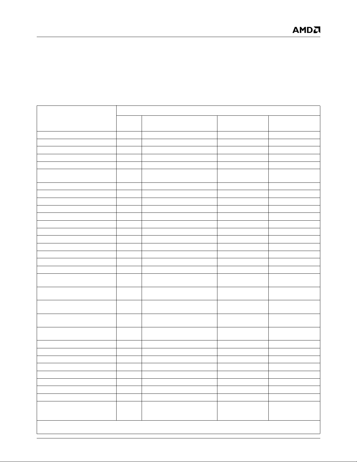
Application Note
Revision 1.0 - April 2001 - Confidential
8.2.1 Power Management Register
Programming Summary
Table 8-10 provides a programming register summary of
the device idle timers, address traps, and general purpose
I/O pins. The tables that follow, provide the bit formats for
the bits listed in the summary. For complete bit in formation
regarding the registers listed in Table 8-10, refer to the
AMD Geode™ CS5530A Companion Device Data Book.
Table 8-10. Device Power Management Programming Summary
Located at F0 Index xxh Unless Otherwise Noted
Device Power
Management Resource
Global Timer Enable 80h[1] N/A N/A N/A
Keyboard / Mouse Idle Timer 81h[3] 93h[1:0] 85h[3] F5h[3]
Parallel / Serial Idle Timer 81h[2] 93h[1:0] 85h[2] F5h[2]
Floppy Disk Idle Timer 81h[1] 9Ah[15:0], 93h[7] 85h[1] F5h[1]
Video Idle Timer (Note 1) 81h[7] A6h[15:0] 85h[7] F5h[7]
VGA Timer (Note 2) 83h[3] 8Eh[7:0] F1BAR+Memory
Primary Hard Disk Idle Timer 81h[0] 98h[15:0], 93h[5] 85h[0] F5h[0]
Secondary Hard Disk Idle Timer 83h[7] ACh[15:0], 93h[4] 86h[4] F6h[4]
User Defined Device 1 Idle Timer 81h[4] A0h[15:0], C0h[31:0], CCh[7:0] 85h[4] F5h[4]
User Defined Device 2 Idle Timer 81h[5] A2h[15:0], C4h[31:0], CDh[7:0] 85h[5] F5h[5]
User Defined Device 3 Idle Timer 81h[6] A4h[15:0], C8h[31:0], CEh[7:0] 85h[6] F5h[6]
Global Trap Enable 80h[2] N/A N/A N/A
Keyboard / Mouse Trap 82h[3] 9Eh[15:0] 93h[1:0] 86h[3] F6h[3]
Parallel / Serial Trap 82h[2] 9Ch[15:0], 93h[1:0] 86h[2] F6h[2]
Floppy Disk Trap 82h[1] 93h[7] 86h[1] F6h[1]
Video Access Trap 82h[7] N/A 86h[7] F6h[7]
Primary Hard Disk Trap 82h[0] 93h[5] 86h[0] F6h[0]
Secondary Hard Disk Trap 83h[6] 93h[4] 86h[5] F6h[5]
User Defined Device 1 Trap 82h[4] C0h[31:0], CCh[7:0] F1BAR+Memory
User Defined Device 2 Trap 82h[5] C4h[31:0], CDh[7:0] F1BAR+Memory
User Defined Device 3 Trap 82h[6] C8h[31:0], CEh[7:0] F1BAR+Memory
General Purpose Timer 1 83h[0] 88h[7:0], 89h[7:0], 8Bh[4] F1BAR+Memory
General Purpose Timer 2 83h[1] 8Ah[7:0], 8Bh[5,3,2] F1BAR+Memory
GPIO7 Pin N/A 90h[7], 91h[7], 92h[7], 97h[7,3] 91h[7] N/A
GPIO6 Pin N/A 90h[6], 91h[6], 92h[6] 87h[4,3], 91h[6] F7h[4,3]
GPIO5 Pin N/A 90h[5], 91h[5], 97h[6,2] 91h[5] N/A
GPIO4 Pin N/A 90h[4], 91h[4], 97h[5,1] 91h[4] N/A
GPIO3 Pin N/A 90h[3], 91h[3], 97h[4,0] 91h[3] N/A
GPIO2 Pin N/A 90h[2], 91h[2], 92h[5,2] 87h[7], 91h[2] F7h[7]
GPIO1 Pin N/A 90h[1], 91h[1] 92h[4,1] 87h[6], 91h[1] F7h[6]
GPIO0 Pin N/A 90h[0], 91h[0], 92h[3,0] 87h[5], 91h[0] F7h[5]
Suspend Modulation OFF/ON
Video Speedup
IRQ Speedup
Note: 1. This function is used for Suspend determination.
2. This function is used for SoftVGA, not power management. It is not affected by Global Power Enable.
Enable Configuration
96h[0]
80h[4]
80h[3]
94h[7:0]/95h[7:0]
8Dh[7:0]
8Ch[7:0]
Second Level SMI
Status/No Clear
Offset 00h[6]
Offset 04h[2]
Offset 04h[3]
Offset 04h[4]
Offset 04h[0]
Offset 04h[1]
N/A
A8h[15:0]
N/A
Second Level SMI
Status/With Clear
F1BAR+Memory
Offset 02h[6]
F1BAR+Memory
Offset 06h[2]
F1BAR+Memory
Offset 06h[3]
F1BAR+Memory
Offset 06h[4]
F1BAR+Memory
Offset 06h[0]
F1BAR+Memory
Offset 06h[1]
N/A
N/A
N/A
AMD Geode™ GX1 Processor/CS5530A Companion Device Power Management Implementations 49
Page 50
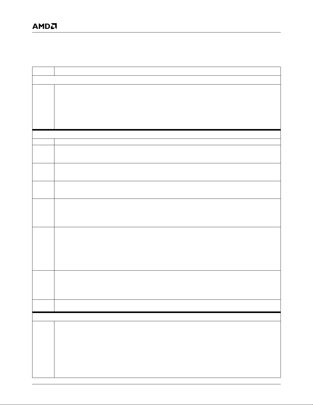
Application Note
Revision 1.0 - April 2001 - Confidential
Table 8-11. General Purpose Timers and Control Registers
Bit Description
F0 Index 88h General Purpose Timer 1 Count Register (R/W) Reset Value = 00h
7:0 General Purpose Timer 1 Count: This register holds the load value for GP Timer 1. This value can represent either an 8-
bit or 16-bit timer (selected at F0 Index 8Bh[4]). It is loaded into the timer when the timer is enabled (F0 Index 83h[0] =1).
Once enabled, an enabled event (configured in F0 Index 89h[6:0]) reloads the timer.
The timer is decremented with each clock of the configured timebase. Upon expiration of the timer , an SMI is gener ated and
the top level SMI status is reported at F1BAR+Memory Offset 00h/02h[9]. The second level SMI status is reported at
F1BAR+Memory Offset 04h/06h[0]).
Once expired, this timer must be re-initialized by either disabling and enabling it, or writing a new count value here.
This timer’s timebase can be configured as 1 msec or 1 sec at F0 Index 89h[7].
F0 Index 89h General Purpose Timer 1 Control Register (R/W) Reset Value = 00h
7 Timebase for General Purpose Timer 1: Selects timebase for GP Timer 1 (F0 Index 88h). 0 = 1 sec; 1 = 1 msec.
6 Re-trigger General Purpose Timer 1 on User Defined Device 3 (UDEF3) Activity: 0 = Disable; 1 = Enable.
Any access to the configured (memory or I/O) address range for UDEF3 reloads GP Timer 1. UDEF3 address
programming is at F0 Index C8h (base address register) and CEh (control register).
5 Re-trigger General Purpose Timer 1 on User Defined Device 2 (UDEF2) Activity: 0 = Disable; 1 = Enable.
Any access to the configured (memory or I/O) address range for UDEF2 reloads GP Timer 1. UDEF2 address
programming is at F0 Index C4h (base address register) and CDh (control register).
4 Re-trigger General Purpose Timer 1 on User Defined Device 1 (UDEF1) Activity: 0 = Disable; 1 = Enable.
Any access to the configured (memory or I/O) address range for UDEF1 reloads GP Timer 1. UDEF1 address
programming is at F0 Index C0h (base address register) and CCh (control register)
3 Re-trigger General Purpose Timer 1 on Keyboard or Mouse Activity: 0 = Disable; 1 = Enable
Any access to the keyboard or mouse I/O address range (listed below) reloads GP Timer 1.
Keyboard Controller: I/O Ports 060h/064h
COM1: I/O Port 3F8h-3FFh (if F0 Index 93h[1:0] = 10 this range is included)
COM2: I/O Port 2F8h-2FFh (if F0 Index 93h[1:0] = 11 this range is included)
2 Re-trigger General Purpose Timer 1 on Parallel/Serial Port Activity: 0 = Disable; 1 = Enable.
Any access to the parallel or serial port I/O address range (listed below) reloads the GP Timer 1.
LPT1: I/O Port 378h-37Fh, 778h-77Ah
LPT2: I/O Port 278h-27Fh, 678h-67Ah
COM1: I/O Port 3F8h-3FFh (if F0 Index 93h[1:0] = 10 this range is excluded)
COM2: I/O Port 2F8h-2FFh (if F0 Index 93h[1:0] = 11 this range is excluded)
COM3: I/O Port 3E8h-3EFh
COM4: I/O Port 2E8h-2EFh
1 Re-trigger General Purpose Timer 1 on Floppy Disk Activity: 0 = Disable; 1 = Enable.
Any access to the floppy disk drive address ranges (listed below) reloads GP Timer 1.
Primary floppy disk: I/O Port 3F2h, 3F4h, 3F5h, and 3F7
Secondary floppy disk: I/O Port 372h, 373h, 375h, and 377h
The active floppy drive is configured via F0 Index 93h[7].
0 Re-trigger General Purpose Timer 1 on Primary Hard Disk Activity: 0 = Disable; 1 = Enable.
Any access to the primary hard disk drive address range selected in F0 Index 93h[5] reloads GP Timer 1.
F0 Index 8Ah General Purpose Timer 2 Count Register (R/W) Reset Value = 00h
7:0 General Purpose Timer 2 Count: This register holds the load value for GP Timer 2. This value can represent either an 8-
bit or 16-bit timer (configured in F0 Index 8Bh[5]). It is loaded into the timer when the timer is enabled (F0 Index 83h[1] = 1).
Once the timer is enabled and a transition occurs on GPIO7, the timer is re-loaded.
The timer is decremented with each clock of the configured timebase. Upon expiration of the timer , an SMI is gener ated and
the top level of status is F1BAR+Memory Offset 00h/02h[9] and the second level of status is reported in F1BAR+Memory
Offset 04h/06h[1]).
Once expired, this timer must be re-initialized by either disabling and enabling it, or writing a new count value here.
For GPIO7 to act as the reload for this timer , it m ust be enabled as such (F0 Inde x 8Bh[2]) and be configured as an input (F0
Index 90h[7]).
This timer’s timebase can be configured as 1 msec or 1 sec in F0 Index 8Bh[3].
50 AMD Geode™ GX1 Processor/CS5530A Companion Device Power Management Implementations
Page 51
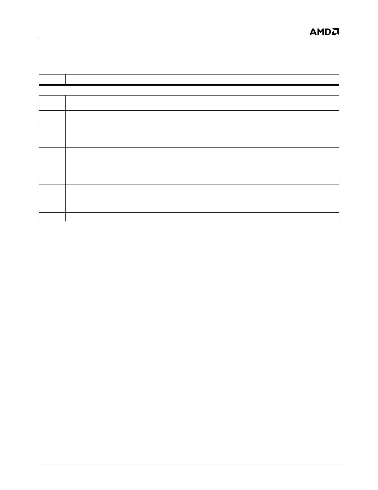
Application Note
Revision 1.0 - April 2001 - Confidential
Table 8-11. General Purpose Timers and Control Registers (Continued)
Bit Description
F0 Index 8Bh General Purpose Timer 2 Control Register (R/W) Reset Value = 00h
7 Re-trigger General Purpose Timer 1 on Secondary Hard Disk Activity: 0 = Disable; 1 = Enable.
Any access to the secondary hard disk drive address range selected in F0 Index 93h[4] reloads GP Timer 1.
6 VGA Timer Base: Selects timebase for VGA Timer Register (F0 Index 8Eh). 0 = 1 ms; 1 = 32 µs.
5 General Purpose Timer 2 Shift: GP Timer 2 is treated as an 8-bit or 16-bit timer. 0 = 8-bit; 1 = 16-bit.
As an 8-bit timer, the count value is loaded into GP Timer 2 Count Register (F0 Index 8Ah).
As a 16-bit timer, the value loaded into GP Timer 2 Count Register is shifted left by eight bits, the lower eight bits become
zero, and this 16-bit value is used as the count for GP Timer 2.
4 General Purpose Timer 1 Shift: GP Timer 1 is treated as an 8-bit or 16-bit timer. 0 = 8-bit; 1 = 16-bit.
As an 8-bit timer, the count value is that loaded into GP Timer 1 Count Register (F0 Index 88h).
As a 16-bit timer, the value loaded into GP Timer 1 Count Register is shifted left by eight bit, the lower eight bits become
zero, and this 16-bit value is used as the count for GP Timer 1.
3 Timebase for General Purpose Timer 2: Selects timebase for GP Timer 2 (F0 Index 8Ah). 0 = 1 sec; 1 = 1 msec.
2 Re-trigger General Purpose Timer 2 on GPIO7 Pin Transition: A configured transition on the GPIO7 pin reloads GP
Timer 2 (F0 Index 8Ah). 0 = Disable; 1 = Enable.
F0 Index 92h[7] selects whether a rising- or a falling-edge transition acts as a reload. For GPIO7 to work here, it must first be
configured as an input (F0 Index 90h[7] = 0).
1:0 Reserved: Set to 0.
AMD Geode™ GX1 Processor/CS5530A Companion Device Power Management Implementations 51
Page 52
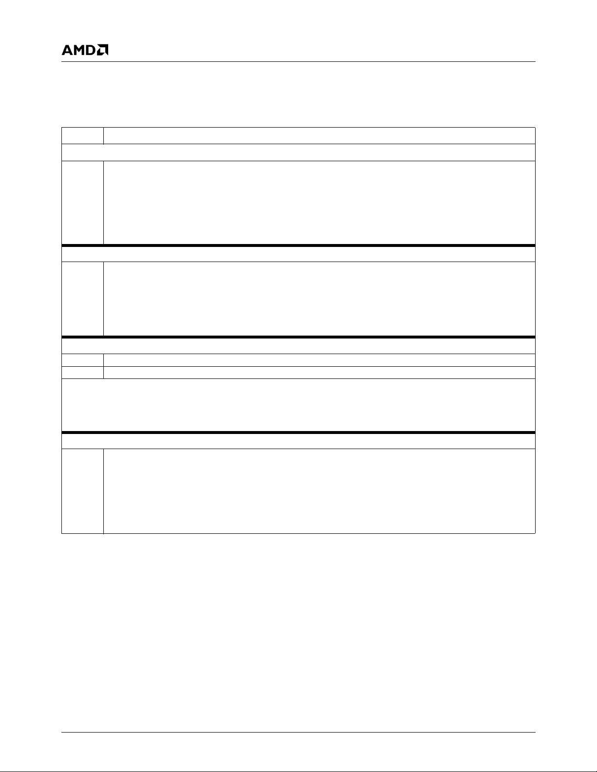
Application Note
Revision 1.0 - April 2001 - Confidential
Table 8-12. Keyboard/Mouse Idle Timer and Trap Related Registers
Bit Description
F0 Index 81h Power Management Enable Register 2 (R/W) Reset Value = 00h
3 Keyboard/Mouse Idle Timer Enable: Load timer from Keyboard/Mouse Idle Timer Count Register (F0 Index 9Eh) and gen-
erate an SMI when the timer expires. 0 = Disable; 1 = Enable.
If an access occurs in the address ranges (listed below) the timer is reloaded with the programmed count.
Keyboard Controller: I/O Ports 060h/064h
COM1: I/O Port 3F8h-3FFh (if F0 Index 93h[1:0] = 10 this range is included)
COM2: I/O Port 2F8h-2FFh (if F0 Index 93h[1:0] = 11 this range is included)
Top level SMI status is reported at F1BAR+Memory Offset 00h/02h[0].
Second level SMI status is reported at F0 Index 85h/F5h[3].
F0 Index 82h Power Management Enable Register 3 (R/W) Reset Value = 00h
3 Keyboard/Mouse Trap: 0 = Disable; 1 = Enable.
If this bit is enabled and an access occurs in the address ranges (listed below) an SMI is generated.
Keyboard Controller: I/O Ports 060h/064h
COM1: I/O Port 3F8h-3FFh (if F0 Index 93h[1:0] = 10 this range is included)
COM2: I/O Port 2F8h-2FFh (if F0 Index 93h[1:0] = 11 this range is included)
Top level SMI status is reported at F1BAR+Memory Offset 00h/02h[0].
Second level SMI status is reported at F0 Index 86h/F6h[3].
F0 Index 93h Miscellaneous Device Control Register (R/W) Reset Value = 00h
1 Mouse on Serial Enable: Mouse is present on a serial port. 0 = No; 1 = Yes. (Note)
0 Mouse Port Select: Selects which serial port the mouse is attached to. 0 = COM1; 1 = COM2. (Note)
Note: Bits 1 and 0 - If a mouse is attached to a serial port (bit 1 = 1), that port is removed from the serial device list being used to
monitor serial port access for power management purposes and added to the keyboard/mouse decode. This is done because a
mouse, along with the keyboard, is considered an input device and is used only to determine when to blank the screen.
These bits determine the decode used for the Keyboard/Mouse Idle Timer Count Register (F0 Index 9Eh) as well as the Parallel/Serial Port Idle Timer Count Register (F0 Index 9Ch).
F0 Index 9Eh-9Fh Keyboard / Mouse Idle Timer Count Register (R/W) Reset Value = 0000h
15:0 Keyboard / Mouse Idle Timer Count: The idle timer loaded from this register determines when the keyboard and mouse
are not in use so that the LCD screen can be blanked. The 16-bit value programmed here represents the period of inactivity
for these ports after which the system is alerted via an SMI. The timer is automatically reloaded with the count value when-
ever an access occurs to either the keyboard or mouse I/O address spaces, including the mouse serial port address space
when a mouse is enabled on a serial port. The timer uses a 1 second timebase.
To enable this timer set F0 Index 81h[3] = 1.
Top level SMI status is reported at F1BAR+Memory Offset 00h/02h[0].
Second level SMI status is reported at F0 Index 85h/F5h[3].
52 AMD Geode™ GX1 Processor/CS5530A Companion Device Power Management Implementations
Page 53
Application Note
Revision 1.0 - April 2001 - Confidential
Table 8-13. Parallel/Serial Idle Timer and Trap Related Registers
Bit Description
F0 Index 81h Power Management Enable Register 2 (R/W) Reset Value = 00h
2 Parallel/Serial Idle Timer Enable: Load timer from Parallel/Serial Port Idle Timer Count Register (F0 Index 9Ch) and gen-
erate an SMI when the timer expires. 0 = Disable; 1 = Enable.
If an access occurs in the address ranges (listed below) the timer is reloaded with the programmed count.
LPT1: I/O Port 378h-37Fh, 778h-77Ah
LPT2: I/O Port 278h-27Fh, 678h-67Ah
COM1: I/O Port 3F8h-3FFh (if F0 Index 93h[1:0] = 10 this range is excluded)
COM2: I/O Port 2F8h-2FFh (if F0 Index 93h[1:0] = 11 this range is excluded)
COM3: I/O Port 3E8h-3EFh
COM4: I/O Port 2E8h-2EFh
Top level SMI status is reported at F1BAR+Memory Offset 00h/02h[0].
Second level SMI status is reported at F0 Index 85h/F5h[2].
F0 Index 82h Power Management Enable Register 3 (R/W) Reset Value = 00h
2 Parallel/Serial Trap: 0 = Disable; 1 = Enable.
If this bit is enabled and an access occurs in the address ranges (listed below) an SMI is generated.
LPT1: I/O Port 378h-37Fh, 778h-77Ah
LPT2: I/O Port 278h-27Fh, 678h-67Ah
COM1: I/O Port 3F8h-3FFh (if F0 Index 93h[1:0] = 10 this range is excluded)
COM2: I/O Port 2F8h-2FFh (if F0 Index 93h[1:0] = 11 this range is excluded)
COM3: I/O Port 3E8h-3EFh
COM4: I/O Port 2E8h-2EFh
Top level SMI status is reported at F1BAR+Memory Offset 00h/02h[0].
Second level SMI status is reported at F0 Index 86h/F6h[2].
F0 Index 93h Miscellaneous Device Control Register (R/W) Reset Value = 00h
1 Mouse on Serial Enable: Mouse is present on a serial port. 0 = No; 1 = Yes. (Note)
0 Mouse Port Select: Selects which serial port the mouse is attached to. 0 = COM1; 1 = COM2. (Note)
Note: Bits 1 and 0 - If a mouse is attached to a serial port (bit 1 = 1), that port is removed from the serial device list being used to
monitor serial port access for power management purposes and added to the keyboard/mouse decode. This is done because a
mouse, along with the keyboard, is considered an input device and is used only to determine when to blank the screen.
These bits determine the decode used for the Keyboard/Mouse Idle Timer Count Register (F0 Index 9Eh) as well as the Parallel/Serial Port Idle Timer Count Register (F0 Index 9Ch).
F0 Index 9Ch-9Dh Parallel / Serial Idle Timer Count Register (R/W) Reset Value = 0000h
15:0 Parallel / Serial Idle Timer Count: The idle timer loaded from this register is used to determine when the parallel and serial
ports are not in use so that the ports can be power managed. The 16-bit value programmed here represents the period of
inactivity for these ports after which the system is alerted via an SMI. T he timer is automatically reloaded with the count
value whenever an access occurs to the parallel (LPT) or serial (COM) I/O address spaces. If the mouse is enabled on a
serial port, that port is not considered here. The timer uses a 1 second timebase.
To enable this timer set F0 Index 81h[2] = 1.
Top level SMI status is reported at F1BAR+Memory Offset 00h/02h[0].
Second level SMI status is reported at F0 Index 85h/F5h[2].
AMD Geode™ GX1 Processor/CS5530A Companion Device Power Management Implementations 53
Page 54
Application Note
Revision 1.0 - April 2001 - Confidential
Table 8-14. Floppy Disk Idle Timer and Trap Related Registers
Bit Description
F0 Index 81h Power Management Enable Register 2 (R/W) Reset Value = 00h
1 Floppy Disk Idle Timer Enable: Load timer from Floppy Disk Idle Timer Count Register (F0 Index 9Ah) and generate an
SMI when the timer expires. 0 = Disable; 1 = Enable.
If an access occurs in the address ranges (listed below) the timer is reloaded with the programmed count.
Primary floppy disk: I/O Port 3F2h, 3F4h, 3F5h, and 3F7
Secondary floppy disk: I/O Port 372h, 373h, 375h, and 377h
Top level SMI status is reported at F1BAR+Memory Offset 00h/02h[0].
Second level SMI status is reported at F0 Index 85h/F5h[1].
F0 Index 82h Power Management Enable Register 3 (R/W) Reset Value = 00h
1 Floppy Disk Trap: 0 = Disable; 1 = Enable.
If this bit is enabled and an access occurs in the address ranges (listed below) an SMI is generated.
Primary floppy disk: I/O Port 3F2h, 3F4h, 3F5h, or 3F7
Secondary floppy disk: I/O Port 372h, 373h, 375h, or 377h
Top level SMI status is reported at F1BAR+Memory Offset 00h/02h[0].
Second level SMI status is reported at F0 Index 86h/F6h[1].
F0 Index 93h Miscellaneous Device Control Register (R/W) Reset Value = 00h
7 Floppy Drive Port Select: All system resources used to power manage the floppy drive use the primary or secondary FDC
addresses for decode. 0 = Primary; 1 = Primary and Secondary.
F0 Index 9Ah-9Bh Floppy Disk Idle Timer Count Register (R/W) Reset Value = 0000h
15:0 Floppy Disk Idle Timer Count: The idle timer loaded from this register is used to determine when the floppy disk drive is
not in use so that it can be powered down. The 16-bit value programmed here represents the period of floppy disk drive
inactivity after which the system is alerted via an SMI. The timer is automatically reloaded with the count value whenever an
access occurs to any of I/O Ports 3F2h, 3F4h, 3F5h, and 3F7h (primary) or 372h, 374h, 375h, and 377h (secondary). The
timer uses a 1 second timebase.
To enable this timer set F0 Index 81h[1] = 1.
Top level SMI status is reported at F1BAR+Memory Offset 00h/02h[0].
Second level SMI status is reported at F0 Index 85h/F5h[1].
Table 8-15. Primary Hard Disk Idle Timer and Trap Related Registers
Bit Description
F0 Index 81h Power Management Enable Register 2 (R/W) Reset Value = 00h
0 Primary Hard Disk Idle Timer Enable: Load timer from Primary Hard Disk Idle Timer Count Register (F0 Index 98h) and
generate an SMI when the timer expires. 0 = Disable; 1 = Enable.
If an access occurs in the address ranges selected in F0 Index 93h[5], the timer is reloaded with the programmed count.
Top level SMI status is reported at F1BAR+Memory Offset 00h/02h[0].
Second level SMI status is reported at F0 Index 85h/F5h[0].
F0 Index 82h Power Management Enable Register 3 (R/W) Reset Value = 00h
0 Primary Hard Disk Trap: 0 = Disable; 1 = Enable.
If this bit is enabled and an access occurs in the address ranges selected in F0 Index 93h[5], an SMI is generated.
Top level SMI status is reported at F1BAR+Memory Offset 00h/02h[0].
Second level SMI status is reported at F0 Index 86h/F6h[0].
F0 Index 93h Miscellaneous Device Control Register (R/W) Reset Value = 00h
5 Partial Primary Hard Disk Decode: This bit is used to restrict the addresses that are decoded as primary hard disk
accesses.
0 = Power management monitors all reads and writes I/O Port 1F0h-1F7h, 3F6h
1 = Power management monitors only writes to I/O Port 1F6h and 1F7h
54 AMD Geode™ GX1 Processor/CS5530A Companion Device Power Management Implementations
Page 55
Application Note
Revision 1.0 - April 2001 - Confidential
Table 8-15. Primary Hard Disk Idle Timer and Trap Related Registers
Bit Description
F0 Index 98h-99h Primary Hard Disk Idle Timer Count Register (R/W) Reset Value = 0000h
15:0 Primary Hard Disk Idle Timer Count: The idle timer loaded from this register is used to determine when the primary hard
disk is not in use so that it can be powered down. The 16-bit value programmed here represents the period of primary hard
disk inactivity after which the system is alerted via an SMI. The timer is automatically reloaded with the count value when-
ever an access occurs to the configured primary hard disk’s data port (configured in F0 Index 93h[5]). The timer uses a 1
second timebase.
To enable this timer set F0 Index 81h[0] = 1.
Top level SMI status is reported at F1BAR+Memory Offset 00h/02h[0].
Second level SMI status is reported at F0 Index 85h/F5h[0].
Table 8-16. Secondary Hard Disk Idle Timer and Trap Related Registers
Bit Description
F0 Index 83h Power Management Enable Register 4 (R/W) Reset Value = 00h
7 Secondary Hard Disk Idle Timer Enable: Load timer from Secondary Hard Disk Idle Timer Count Register (F0 Index ACh)
and generate an SMI when the timer expires. 0 = Disable; 1 = Enable.
If an access occurs in the address ranges selected in F0 Index 93h[4], the timer is reloaded with the programmed count.
Top level SMI status is reported at F1BAR+Memory Offset 00h/02h[0].
Second level SMI status is reported at F0 Index 86h/F6h[4].
6 Secondary Hard Disk Trap: 0 = Disable; 1 = Enable.
If this bit is enabled and an access occurs in the address ranges selected in F0 Index 93h[4], an SMI is generated.
Top level SMI status is reported at F1BAR+Memory Offset 00h/02h[0].
Second level SMI status is reported at F0 Index 86h/F6h[5].
F0 Index 93h Miscellaneous Device Control Register (R/W) Reset Value = 00h
4 Partial Secondary Hard Disk Decode: This bit is used to restrict the addresses that are decoded as secondary hard Disk
accesses.
0 = Power management monitors all reads and writes I/O Port 170h-177h, 376h
1 = Power management monitors only writes to I/O Port 176h and 177h
F0 Index ACh-ADh Secondary Hard Disk Idle Timer Count Register (R/W) Reset Value = 0000h
15:0 Secondary Hard Disk Idle Timer Count: The idle timer loaded from this register is used to determine when the secondary
hard disk is not in use so that it can be powered down. The 16-bit value programmed here represents the period of second-
ary hard disk inactivity after which the system is alerted via an SMI. The timer is automatically reloaded with the count value
whenever an access occurs to the configured secondary hard disk’s data port (configured in F0 Index 93h[4]). The timer
uses a 1 second timebase.
To enable this timer set F0 Index 83h[7] = 1.
Top level SMI status is reported at F1BAR+Memory Offset 00h/02h[0].
Second level SMI status is reported at F0 Index 86h/F6h[4].
AMD Geode™ GX1 Processor/CS5530A Companion Device Power Management Implementations 55
Page 56
Application Note
Revision 1.0 - April 2001 - Confidential
Table 8-17. User Defined Device 1 (UDEF1) Idle Timer and Trap Related Registers
Bit Description
F0 Index 81h Power Management Enable Register 2 (R/W) Reset Value = 00h
4 User Defined Device 1 (UDEF1) Idle Timer Enable: Load timer from UDEF1 Idle Timer Count Register (F0 Index A0h) and
generate an SMI when the timer expires. 0 = Disable; 1 = Enable.
If an access occurs in the programmed address range the timer is reloaded with the programmed count.
UDEF1 address programming is at F0 Index C0h (base address register) and CCh (control register).
Top level SMI status is reported at F1BAR+Memory Offset 00h/02h[0].
Second level SMI status is reported at F0 Index 85h/F5h[4].
F0 Index 82h Power Management Enable Register 3 (R/W) Reset Value = 00h
4 User Defined Device 1 (UDEF1) Trap: 0 = Disable; 1 = Enable.
If this bit is enabled and an access occurs in the programmed address range an SMI is generated. UDEF1 address
programming is at F0 Index C0h (base address register), and CCh (control register).
Top level SMI status is reported at F1BAR+Memory Offset 00h/02h[9].
Second level SMI status is reported at F1BAR+Memory Offset 04h/06h[2].
Index A0h-A1h User Defined Device 1 Idle Timer Count Register (R/W) Reset Value = 0000h
15:0 User Defined Device 1 (UDEF1) Idle Timer Count: The idle timer loaded from this register determines when the device
configured as UDEF1 is not in use so that it can be power managed. The 16-bit value programmed here represents the
period of inactivity for this device after which the system is alerted via an SMI. The timer is automatically reloaded with the
count value whenever an access occurs to memory or I/O address space configured at F0 Index C0h (base address regis-
ter) and F0 Index CCh (control register). The timer uses a 1 second timebase.
To enable this timer set F0 Index 81h[4] = 1.
Top level SMI status is reported at F1BAR+Memory Offset 00h/02h[0].
Second level SMI status is reported at F0 Index 85h/F5h[4].
F0 Index C0h-C3h User Defined Device 1 Base Address Register (R/W) Reset Value = 00000000h
31:0 User Defined Device 1 (UDEF1) Base Address [31:0]: This 32-bit register supports power management (trap and idle
timer resources) for a PCMCIA slot or some other device in the system. The value written is used as the address compara-
tor for the device trap/timer logic. The device can be memory or I/O mapped (configured in F0 Index CCh).
F0 Index CCh User Defined Device 1 Control Register (R/W) Reset Value = 00h
7 Memory or I/O Mapped: User Defined Device 1 is: 0 = I/O; 1 = Memory.
6:0 Mask
If bit 7 = 0 (I/O):
Bit 6 0 = Disable write cycle tracking
1 = Enable write cycle tracking
Bit 5 0 = Disable read cycle tracking
1 = Enable read cycle tracking
Bits 4:0 Mask for address bits A[4:0]
If bit 7 = 1 (M/IO):
Bits 6:0 Mask for address memory bits A[15:9] (512 bytes min. and 64 KB max.) and A[8:0] are ignored.
Note: A “1” in a mask bit means that the address bit is ignored for comparison.
56 AMD Geode™ GX1 Processor/CS5530A Companion Device Power Management Implementations
Page 57
Application Note
Revision 1.0 - April 2001 - Confidential
Table 8-18. User Defined Device 2 (UDEF2) Idle Timer and Trap Related Registers
Bit Description
F0 Index 81h Power Management Enable Register 2 (R/W) Reset Value = 00h
5 User Defined Device 2 (UDEF2) Idle Timer Enable: Load timer from UDEF2 Idle Timer Count Register (F0 Index A2h) and
generate an SMI when the timer expires. 0 = Disable; 1 = Enable.
If an access occurs in the programmed address range the timer is reloaded with the programmed count.
UDEF2 address programming is at F0 Index C4h (base address register) and CDh (control register).
Top level SMI status is reported at F1BAR+Memory Offset 00h/02h[0].
Second level SMI status is reported at F0 Index 85h/F5h[5].
F0 Index 82h Power Management Enable Register 3 (R/W) Reset Value = 00h
5 User Defined Device 2 (UDEF2) Trap: 0 = Disable; 1 = Enable.
If this bit is enabled and an access occurs in the programmed address range an SMI is generated. UDEF2 address
programming is at F0 Index C4h (base address register) and CDh (control register).
Top level SMI status is reported at F1BAR+Memory Offset 00h/02h[9].
Second level SMI status is reported at F1BAR+Memory Offset 04h/06h[3].
F0 Index A2h-A3h User Defined Device 2 Idle Timer Count Register (R/W) Reset Value = 0000h
15:0 User Defined Device 2 (UDEF2) Idle Timer Count: The idle timer loaded from this register determines when the device
configured as UDEF2 is not in use so that it can be power managed. The 16-bit value programmed here represents the
period of inactivity for this device after which the system is alerted via an SMI. The timer is automatically reloaded with the
count value whenever an access occurs to memory or I/O address space configured at F0 Index C4h (base address regis-
ter) and F0 Index CDh (control register). The timer uses a 1 second timebase.
To enable this timer set F0 Index 81h[5] = 1.
Top level SMI status is reported at F1BAR+Memory Offset 00h/02h[0].
Second level SMI status is reported at F0 Index 85h/F5h[5].
F0 Index C4h-C7h User Defined Device 2 Base Address Register (R/W) Reset Value = 00000000h
31:0 User Defined Device 2 (UDEF2) Base Address [31:0]: This 32-bit register supports power management (trap and idle
timer resources) for a PCMCIA slot or some other device in the system. The value written is used as the address compara-
tor for the device trap/timer logic. The device can be memory or I/O mapped (configured in F0 Index CDh).
F0 Index CDh User Defined Device 2 Control Register (R/W) Reset Value = 00h
7 Memory or I/O Mapped: User Defined Device 2 is: 0 = I/O; 1 = Memory.
6:0 Mask
If bit 7 = 0 (I/O):
Bit 6 0 = Disable write cycle tracking
1 = Enable write cycle tracking
Bit 5 0 = Disable read cycle tracking
1 = Enable read cycle tracking
Bits 4:0 Mask for address bits A[4:0]
If bit 7 = 1 (M/IO):
Bits 6:0 Mask for address memory bits A[15:9] (512 bytes min. and 64 KB max.) and A[8:0] are ignored.
Note: A “1” in a mask bit means that the address bit is ignored for comparison.
AMD Geode™ GX1 Processor/CS5530A Companion Device Power Management Implementations 57
Page 58
Application Note
Revision 1.0 - April 2001 - Confidential
Table 8-19. User Defined Device 3 (UDEF3) Idle Timer and Trap Related Registers
Bit Description
F0 Index 81h Power Management Enable Register 2 (R/W) Reset Value = 00h
6 User Defined Device 3 (UDEF3) Idle Timer Enable: Load timer from UDEF3 Idle Timer Count Register (F0 Index A4h) and
generate an SMI when the timer expires. 0 = Disable; 1 = Enable.
If an access occurs in the programmed address range the timer is reloaded with the programmed count.
UDEF3 address programming is at F0 Index C8h (base address register) and CEh (control register).
Top level SMI status is reported at F1BAR+Memory Offset 00h/02h[0].
Second level SMI status is reported at F0 Index 85h/F5h[6].
F0 Index 82h Power Management Enable Register 3 (R/W) Reset Value = 00h
6 User Defined Device 3 (UDEF3) Trap: 0 = Disable; 1 = Enable.
If this bit is enabled and an access occurs in the programmed address range an SMI is generated. UDEF3 address
programming is at F0 Index C8h (base address register) and CEh (control register).
Top level SMI status is reported at F1BAR+Memory Offset 00h/02h[9].
Second level SMI status is reported at F1BAR+Memory Offset 04h/06h[4].
F0 Index A4h-A5h User Defined Device 3 Idle Timer Count Register (R/W) Reset Value = 0000h
15:0 User Defined Device 3 (UDEF3) Idle Timer Count: The idle timer loaded from this register determines when the device
configured as UDEF3 is not in use so that it can be power managed. The 16-bit value programmed here represents the
period of inactivity for this device after which the system is alerted via an SMI. The timer is automatically reloaded with the
count value whenever an access occurs to memory or I/O address space configured at F0 Index C8h (base address regis-
ter) and F0 Index CEh (control register). The timer uses a 1 second timebase.
To enable this timer set F0 Index 81h[6] = 1.
Top level SMI status is reported at F1BAR+Memory Offset 00h/02h[0].
Second level SMI status is reported at F0 Index 85h/F5h[6].
F0 Index C8h-CBh User Defined Device 3 Base Address Register (R/W) Reset Value = 00000000h
31:0 User Defined Device 3 (UDEF3) Base Address [31:0]: This 32-bit register supports power management (trap and idle
timer resources) for a PCMCIA slot or some other device in the system. The value written is used as the address compara-
tor for the device trap/timer logic. The device can be memory or I/O mapped (configured in F0 Index CEh).
F0 Index CEh User Defined Device 3 Control Register (R/W) Reset Value = 00h
7 Memory or I/O Mapped: User Defined Device 3 is: 0 = I/O; 1 = Memory.
6:0 Mask
If bit 7 = 0 (I/O):
Bit 6 0 = Disable write cycle tracking
1 = Enable write cycle tracking
Bit 5 0 = Disable read cycle tracking
1 = Enable read cycle tracking
Bits 4:0 Mask for address bits A[4:0]
If bit 7 = 1 (M/IO):
Bits 6:0 Mask for address memory bits A[15:9] (512 bytes min. and 64 KB max.) and A[8:0] are ignored.
Note: A “1” in a mask bit means that the address bit is ignored for comparison.
58 AMD Geode™ GX1 Processor/CS5530A Companion Device Power Management Implementations
Page 59
Application Note
Revision 1.0 - April 2001 - Confidential
Table 8-20. Video Idle Timer and Trap Related Registers
Bit Description
F0 Index 81h Power Management Enable Register 2 (R/W) Reset Value = 00h
7 Video Access Idle Timer Enable: Load timer from Video Idle Timer Count Register (F0 Index A6h) and generate an SMI
when the timer expires. 0 = Disable; 1 = Enable.
If an access occurs in the video address range (sets bit 0 of the GX-series processor’s PSERIAL register) the timer is
reloaded with the programmed count.
Top level SMI status is reported at F1BAR+Memory Offset 00h/02h[0].
Second level SMI status is reported at F0 Index 85h/F5h[7].
F0 Index 82h Power Management Enable Register 3 (R/W) Reset Value = 00h
7 Video Access Trap: 0 = Disable; 1 = Enable.
If this bit is enabled and an access occurs in the video address range (sets bit 0 of the GX-series processor’s PSERIAL
register) an SMI is generated.
Top level SMI status is reported at F1BAR+Memory Offset 00h/02h[0].
Second level SMI status is reported at F0 Index 86h/F6h[7].
F0 Index A6h-A7h Video Idle Timer Count Register (R/W) Reset Value = 0000h
15:0 Video Idle Timer Count: The idle timer loaded from this register determines when the graphics subsystem has been idle as
part of the Suspend determination algorithm. The 16-bit value programmed here represents the period of video inactivity
after which the system is alerted via an SMI. The count in this timer is automatically reset whenever an access occurs to the
graphics controller space. The timer uses a 1 second timebase.
In a GX-series processor based system the graphics controller is embedded in the CPU, so video activity is communicated
to the CS5530A via the serial connection (PSERIAL register, bit 0) from the processor. The CS5530A also detects accesses
to standard VGA space on PCI (3Bxh, 3Cxh, 3Dxh and A000h-B7FFh) in the event an external V GA controller is being used.
To enable this timer set F0 Index 81h[7] = 1.
Top level SMI status is reported at F1BAR+Memory Offset 00h/02h[0].
Second level SMI status is reported at F0 Index 85h/F5h[7].
Table 8-21. VGA Timer Related Registers
Bit Description
F0 Index 83h Power Management Enable Register 4 (R/W) Reset Value = 00h
3 VGA Timer Enable: Turn on VGA Timer and generate an SMI when the timer reaches 0. 0 = Disable; 1 = Enable.
VGA Timer programming is at F0 Index 8Eh and F0 Index 8Bh[6].
To reload the count in the VGA timer, disable it, optionally change the count value in F0 Index 8Eh[7:0], and reenable it
before enabling power management.
SMI Status reporting is at F1BAR+Memory Offset 00h/02h[6] (only).
Although grouped with the power management Idle Timers, the VGA Timer is not a power management function. The VGA
Timer counts whether power management is enabled or disabled.
F0 Index 8Bh General Purpose Timer 2 Control Register (R/W) Reset Value = 00h
6 VGA Timer Base: Selects timebase for VGA Timer Register (F0 Index 8Eh). 0 = 1 ms; 1 = 32 µs.
F0 Index 8Eh VGA Timer Count Register
7:0 VGA Timer Load Value: This register holds the load value for the VGA timer. The value is loaded into the timer when the
timer is enabled (F0 Index 83h[3] = 1). The timer is decremented with each clock of the configured timebase (F0 Index
8Bh[6]). Upon expiration of the timer, an SMI is generated and the status is reported in F1BAR+Memory Offset 00h/02h[6]
(only). Once expired, this timer must be re-initialized by disabling it (F0 Index 83h[3] = 0) and then enabling it (F0 Index
83h[3] = 1). When the count value is changed in this register, the timer must be re-initialized in order for the new value to be
loaded.
This timer’s timebase is selectable as 1 ms (default) or 32 µs. (F0 Index 8Bh).
Note: Although grouped with the power management Idle Timers, the V GA Timer is not a power management function. It is
not affected by the Global Power Management Enable setting at F0 Index 80h[0].
AMD Geode™ GX1 Processor/CS5530A Companion Device Power Management Implementations 59
Page 60

© 2004 Advanced Micro Devices, Inc. All rights reserved.
The contents of this document are provided in connection with Advanced Micro
Devices, Inc. (“AMD”) products. AMD makes no representations or warranties with
respect to the accuracy or completeness of the contents of this publication and
reserves the right to make changes to specifications and product descriptions at
any time without notice. No license, whether express, implied, arising by estoppel
or otherwise, to any intellectual property rights is granted by this publication.
Except as set forth in AMD’s Standard Terms and Conditions of Sale, AMD
assumes no liability whatsoever, and disclaims any express or implied warranty,
relating to its products including, but not limited to, the implied warranty of merchantability, fitness for a particular purpose, or infringement of any intellectual
property right.
AMD’s products are not designed, intended, authorized or warranted for use as
components in systems intended for surgical implant into the body, or in other
applications intended to support or sustain life, or in any other application in which
the failure of AMD’s product could create a situation where personal injury, death,
or severe property or environmental damage ma y occur. AMD reserves the right to
discontinue or make changes to its products at any time without notice.
www.amd.com
One AMD Place
P.O. Box 3453,
Sunnyvale, CA 94088-3453 USA
Tel: 408-732-2400 or 800-538-8450
TWX: 910-339-9280
TELEX: 34-6306
TECHNICAL SUPPORT
USA & Canada: 800-222-9323 or 408-749-5703
USA & Canada: PC Microprocessor: 408-749-3060
USA & Canada Email: [email protected]
Latin America Email: [email protected]
Argentina: 001-800-200-1111, after tone 800-859-4478
Chile: 800-532-853
Mexico: 95-800-222-9323
Europe & UK: +44–0-1276-803299
Fax: +44–0-1276-803298
France: 0800-908-621
Germany: +49–89-450-53199
Italy: 800-877224
Europe Email: [email protected]
Far East Fax: 852-2956-0588
Japan Fax: 81-3-3346-7848
TRADEMARKS
AMD, the AMD Arrow logo, and combinations
thereof, and Geode and Virtual Systems
Architecture are trademarks of
Advanced Micro Devices, Inc.
Microsoft and Windows are registered trademarks
of Microsoft Corporation in the United States
and/or other jurisdictions.
Other product names used in this publication are
for identification purposes only and may be trademarks of their respective companies.
 Loading...