

Page 1

FCC Compliance Statement:
DECLARATION OF CONFOR M I TY
Per FCC Part 2 Section 2. 1077(a)
This equipment has been tested and found to
comply with limits for a Class B digital device,
Responsible Party Name: G.B. T. I NC.
Phone/Fax No: (818) 854-9338/ (818) 854-9339
hereby declares that the product
Product Name:
Model Number:
Conforms to the following specificatio ns:
FCC Part 15, Subpart B, Section 15.107(a) and Section 15.109(a),
Class B Digital Device
Supplementary Information:
This device complies with part 15 o f the FCC Rules. Operation is su bject to the
following two conditions: (1) This device may not cause harmful
and (2) this device must accept any inference received, including
that may cause undesired operation.
Representative P erson's Name: ERIC LU
Signature:
Address: 18305 Valley Blvd., Suite#A
Mother Board
Date: Jan. 22, 2001
LA Puent, CA 91744
GA-7DX
Eric Lu
pursuant to Part 15 of the FCC rules. These
limits are designed to provide reasonable
protection against harmful interference in
residential installations. This equipment
generates, uses, and can radiate radio
frequency energy, and if not installed and used
in accord ance with the instr uctions, may cause
harmful interference to radio communications.
However, there is no guara nte e tha t i nterfer ence
will not occur in a particular installation. If this
equipment does cause interference to radio or
television equipment reception, which can be
determined by turning th e equi pment off and on, the user i s encour aged to try t o
correct the interference by one or more of the following measures:
-Reorient or relocate the receiving antenna
-Move the equipment away from the receiver
-Plug the equipment into an outlet on a circuit different from that to which
the receiver is connected
-Consult the dealer or an experienced radio/television technician for
additional suggestions
You are cautioned that any change or modifications to the equipment not
expressly approve by the party responsible for compliance could void Your
authority to operate such equipment.
This device complies with Part 15 of the FCC Rules. Operation is subjected to
the following two conditions 1) this device may not cause harmful interference
and 2) this device must a ccept any interference received , including interference
that may cause undesired operation.
Page 2

Declaration of Conformity
We, Manufacturer/Importer
(full address)
G.B.T. Technology Träding GMbH
Ausschlager Weg 41, 1F, 20537 Hamburg, Germany
( description of the apparatus, system, installation to which it refers)
(reference to the specification under which conformity is declared)
in accordance with 89/336 EEC-EMC Directive
EN 55011 Limits and methods of measurement EN 61000-3-2* Disturbances in supply systems caused
of radio disturbance characteristics of
industrial, scientific and medical (ISM electrical equipment “Harmonic s”
high frequency equipment
EN55013 Limits and methods of measurement EN61000-3-3* Disturbances in supply systems caused
of radio disturbance characteristics of
broadcast receivers and associated electrical equipment “Voltage fluctuations”
equipment
EN 55014 Limits and methods of measurement EN 50081-1 Generic emission standard Part 1:
of radio disturbance characteristics of Residual, commer ci al and light industry
household electrical appli anc es,
portable tools and similar electrical
apparatus Residual, commerci al and light industry
EN 55015 Limits and methods of measurement EN 55081-2 Generic emission standard Part 2:
of radio disturbance characteristics of Industrial environment
fluorescent lamps and luminaries
EN 55020 Immunity from radio interference of EN 55082-2 Generic immunity standard Part 2:
broadcast receivers and associated Industrial environment
equipment
EN 55022 Limits and methods of measurement ENV 55104 Immunity requirements for household
of radio disturbance characteristics of appliances tools and similar apparatus
information technology equipment
DIN V DE 0855 Cabled distribution systems; Equi pm ent EN 50091- 2 EMC requi r em ents for uninterruptible
part 10 for receiving and/or distribution from power systems (UPS )
part 12 sound and t elevision signals
declare that the product
Mother Board
GA-7DX
is in conformity with
EN60555-2 by household appliances and similar
EN60555-3 by household appliances and similar
EN 50082-1 Generic immunity standard Part 1:
CE marking (EC conformity marking)
The manufacturer also declares the conformity of above mentioned product
with the actual required safety standards in accordance with LVD 73/23 EEC
EN 60065 Safety requirements for mains operated EN 60950 Safety for information technology equipment
electronic and related apparatus for including electrical business equipment
household and similar general use
EN 60335 Safety of household and similar EN 50091-1 General and Safety requirements for
electrical appliances uninterruptible power systems (UPS)
Signature
Date : Jan. 22, 2001 Name : Rex Lin
(Stamp)
Manufacturer/Importer
:
Rex Lin
Page 3

7DX
AMD AthlonTM/DuronTM Socket A Processor
Motherboard
USER'S MANUAL
AMD AthlonTM/DuronTM Socket A Processor Motherboard
REV. 4.0 First Edition
R-40-01-010209
Page 4

Page 5

How This Manual Is Organized
This manual is divided into the following sections:
1) Revision History Manual revision information
2) Item Checklist Product item list
3) Features Product information & specification
4) Hardware Setup Instructions on setting up the motherboard
5) Performance & Block Diagram Product performance & block diagram
6) Suspend to RAM Instructions on STR installation
7) Four Speaker & SPDIF Four Speaker & SPDIF introduction
8) DDR DDR introduction
9) @BIOSTM & EasyTuneIIITM @BIOSTM & EasyTuneIIITM introduction
10) BIOS Setup Instructions on setting up the BIOS
software
11) Appendix General reference
Page 6

Page 7

Table Of Content
Revision History P.1
Item Checklist P.2
Feature Summary P.3
7DX Motherboard Layout P.5
Page Index for CPU Speed Setup/Connectors/Panel and Jumper Definition P.6
Performance List P.24
Block Diagram P.25
Suspend to RAM Installation (Optional) P.26
Four Speaker & SPDIF Introduction (Optional) P.32
DDR Introduction P.38
@BIOSTM Introduction P.39
EasyTuneIIITM Introduction P.40
Memory Installation P.42
Page Index for BIOS Setup P.44
Appendix P.79
Page 8

7DX Motherboard
Revision History
Revision Revision Note Date
3.0 Initial release of the 7DX motherboard user’s manual. Jan. 2001
4.0 Initial release of the 7DX motherboard user’s manual. Feb. 2001
The author assumes no responsibility for any errors or omissions that may appear in this
document nor does the author make a commitment to update the information contained herein.
Third-party brands and names are the property of their respective owners.
Feb. 9, 2001 Taipei, Taiwan, R.O.C
1
Page 9

Item Checklist
The 7DX motherboard
Cable for IDE / floppy device
Diskettes or CD (TUCD) for motherboard driver & utility
7DX user’s manual
Item Checklist
2
Page 10

7DX Motherboard
Feature Summary
Form Factor 30.4 cm x 23.3 cm ATX size form factor
CPU
AMD Athlon
256K/64K L2 cache on die
Supports 600MHz ~ 1GHz and above
TM
/DuronTM (K7) Socket A Processor
Chipset 7DX, consisting of:
AMD 761 Memory/PCI/AGP Controller
VT82C686B PCI Super-I/O Integrated Peripheral
Controller (PSIPC)
Clock Generator ICS 9248-153
200/266 MHz DDR bus speeds
95/100.7/100.9/103/105/110/115/133 MHz system bus
speeds
Supports 100/133 MHz
Memory 2 184-pin DDR DIMM sockets
Supports PC1600 DDR or PC2100 DDR SDRAM
(Support Registered/Unbuffered DDR DIMM)
Supports up to 4GB DRAM (Max)
Supports only 2.5V DDR SDRAM
Supports 72bit ECC type DRAM integrity mode
I/O Control VT82C686B
Slots 1 AGP slot supports 2X/4X mode & AGP 2.0 compliant
5 PCI slots supports 33MHz & PCI 2.2 compliant
1 AMR (Audio Modem Riser) slot
On-Board IDE 2 IDE bus master (UDMA 33/ATA 66/ATA100) IDE
ports for up to 4 ATAPI devices
Supports PIO mode 3, 4, UDMA33/ATA66/ATA100 IDE
& AT API CD-ROM
On-Board
Peripherals
1 floppy port supports 2 FDD with 360K, 720K, 1.2M,
1.44M and 2.88M bytes
1 parallel port supports Normal/EPP/ECP mode
2 serial ports (COM A & COM B)
4 USB ports
1 IrDA connector for IR
Hardware Monitor CPU/System fan revolution detect
CPU/System temperature detect
System voltage detect
CPU overheat shutdown detect
To be continued…
3
Page 11

Features Summary
On-Board Sound
PS/2 Connector
BIOS Licensed AWARD BIOS, 2M bit flash ROM
Additional Features Support Wake-On-LAN (WOL)
Creative CT5880 sound (Optional)
AC’97 CODEC
Line In/Line Out/Mic In/AUX In/CD In/TEL/Game Port
/ Four Speaker & SPDIF (Optional)
PS/2
Support Internal / External Modem Ring On
Support USB KB/MS Wake up from S3-S5
Includes 3 fan power connectors
Poly fuse for keyboard over-current protection
Support STR (Suspend-To-RAM) function (Optional)
Support @BIOS™ and EasyTuneIII™
Keyboard interface and PS/2 Mouse interface
4
Page 12
7DX Motherboard
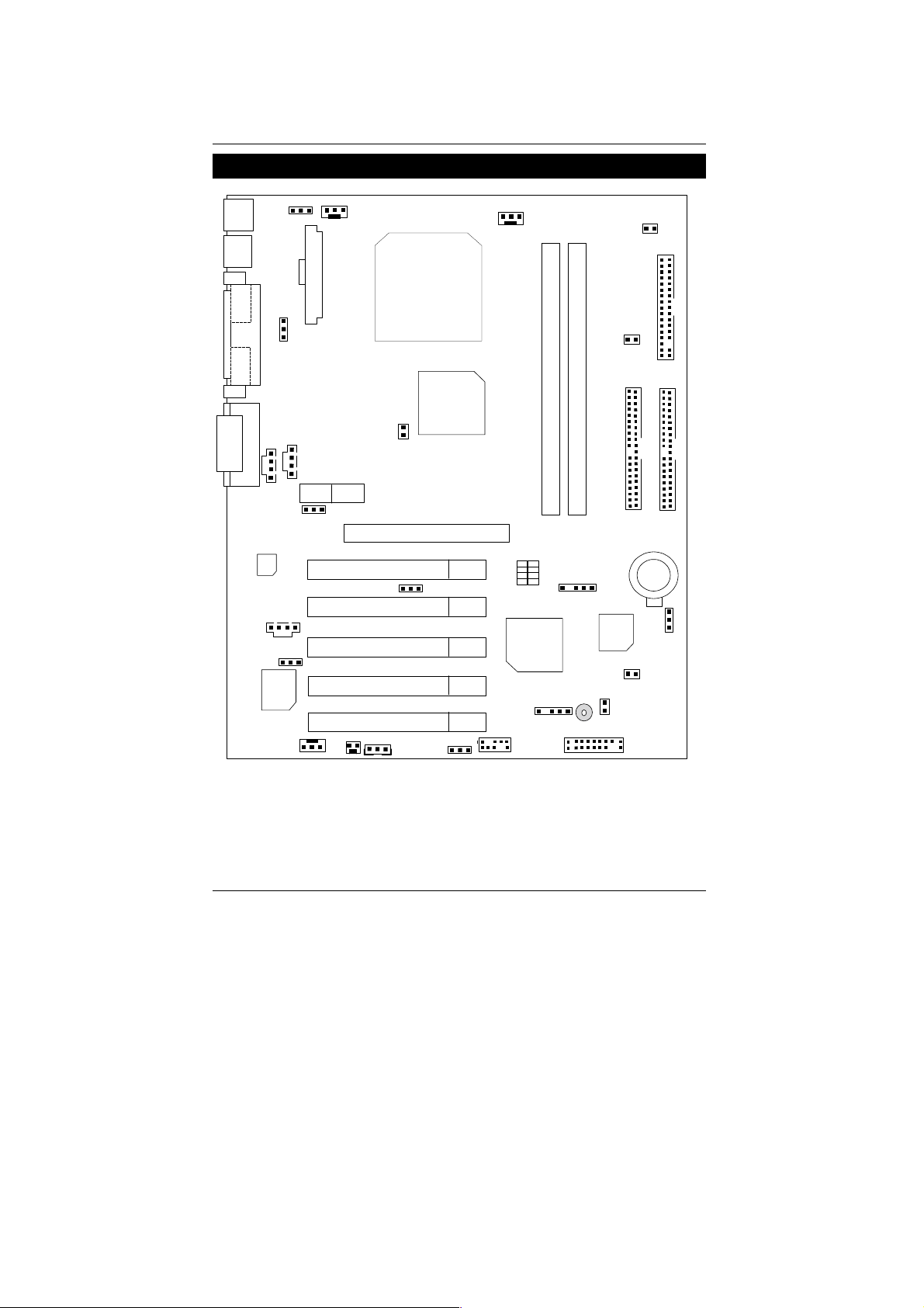
A
7DX Motherboard Layout
PS/2
USB1
COM A
COM B
J6
J15
Socket 462 CPU
ATX POWER
J50
LPT
AMD 761
J17
LED2
FLOPPY
J18
Game & Audio
J24
C97
J23
Creative
CT5880
J26
J16
J27
AGP
J10
J21
7DX
JP1
IDE2
IDE1
DIMM1
DIMM2
SW1
BIOS
J13
BAT1
JP5
J7
J1
VT82C686B
BZ1
J12
J8
USB2
J14
J25
AMR
PCI1
PCI2
PCI3
PCI4
PCI5
J9
5
Page 13
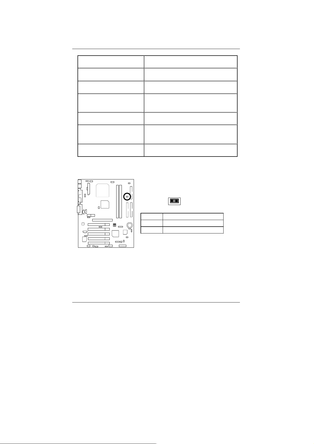
7DX Motherboard Layout
Page Index for CPU Speed Setup/Connectors/Panel and Jumper Definition
Page
CPU Speed Setup P.7
SW1 P.7
Connectors P.8
ATX Power P.8
COM A / COM B / LPT Port P.8
Floppy Connector P.9
Game & Audio Port P.9
IDE 1(Primary) / IDE 2(Secondary) Connector P.10
J1 (External SMBUS Header) P.10
J9 (Ring Power On) P.11
J10 (Wake On LAN) P.11
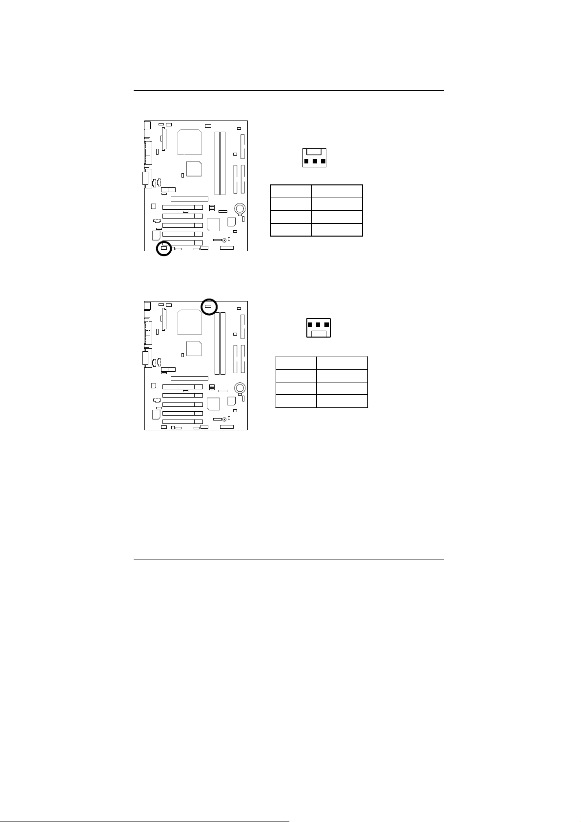
J12 (IR Header) P.12
J15 (Power Fan) P.12
J16 (System Fan) P.13
J17 (CPU Fan) P.13
J21 (Chip Fan) P.14
J23 (TEL) P.14
J24 (CD Audio Line In) P.15
J25 (AUX_IN) P.15
LED2 (DIMM LED) P.16
PS/2 Keyboard & PS/2 Mouse Port P.16
USB1 (Rear USB Port) P.17
USB2 (Front USB Connector) P.17
Panel and Jumper Definition P.18
BAT1 (Battery) P.18
J6 (Rear USB Device Wake up Selection) P.18
J7 (BIOS Write Protect Function) P.19
J8 (Front Panel USB Device Wake up Selection) P.19
J13 (Internal Buzzer Selection) P.20
J14 (2x11 Pins Front Panel) P.20
J18 (STR Enable /Disable Jumper) [Optional] P.21
J26&J27 (Primary CODEC Selection)[For AC97 Only] P.22
J50 (S3 KB/MS Wake up) [Optional] P.22
JP1 (Registered/Unbuffered DDR DIMM Selection) [Optional] P.23
JP5 (Clear CMOS Function) [Optional] P.23
6
Page 14
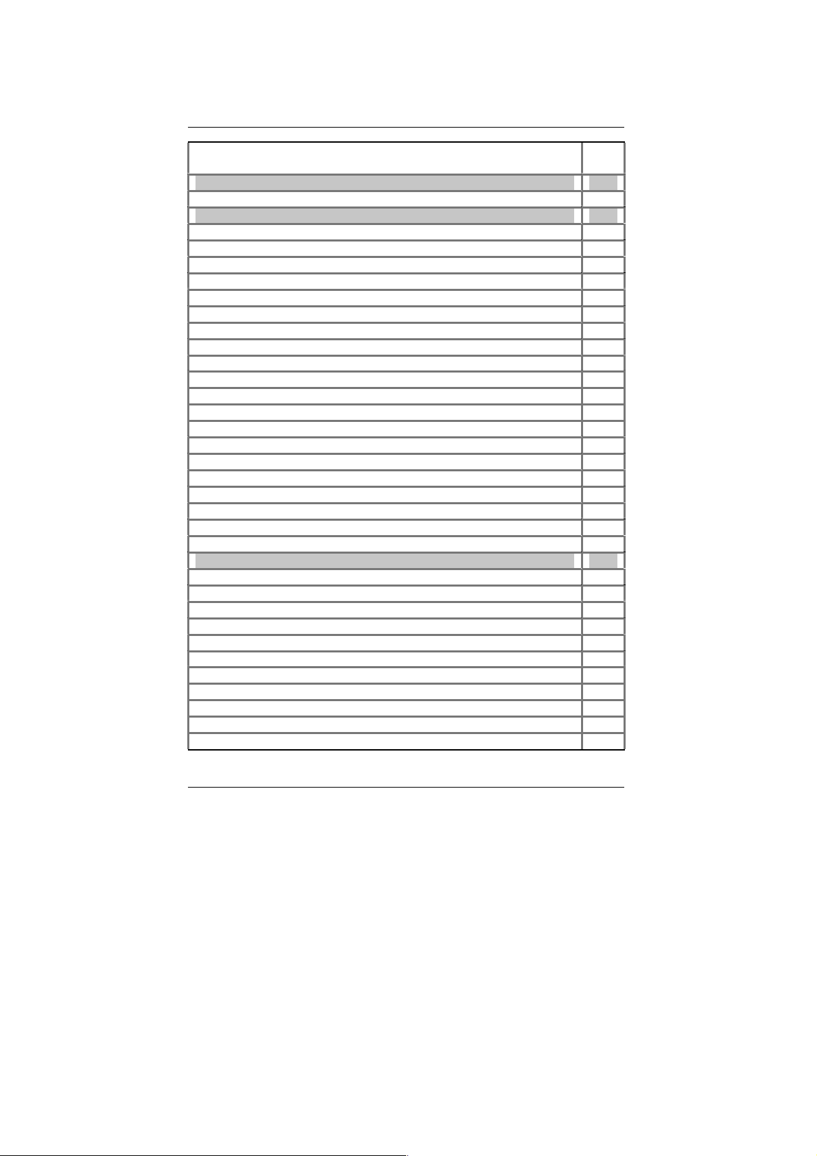
7DX Motherboard
CPU Speed Setup
The system bus speed is selectable at 100~133MHz. The user can select the system bus speed
by DIP switch SW1.
SW1: CPU Speed Setup
Set System Bus Speed
SW1:
O: ON, X: OFF
CPU PCI AGP 1 2 3 4
133 33.3 66.6 O O O O
115 38.3 76.67 X X O X
110 36.67 73.33 X X X X
105 35 70 O X X X
103 34.33 68.67 X O X X
100.9 33.66 67.335 O X O X
100.7 33.57 67.13 O O X X
95 31.67 63.33 X O O X
7
Page 15
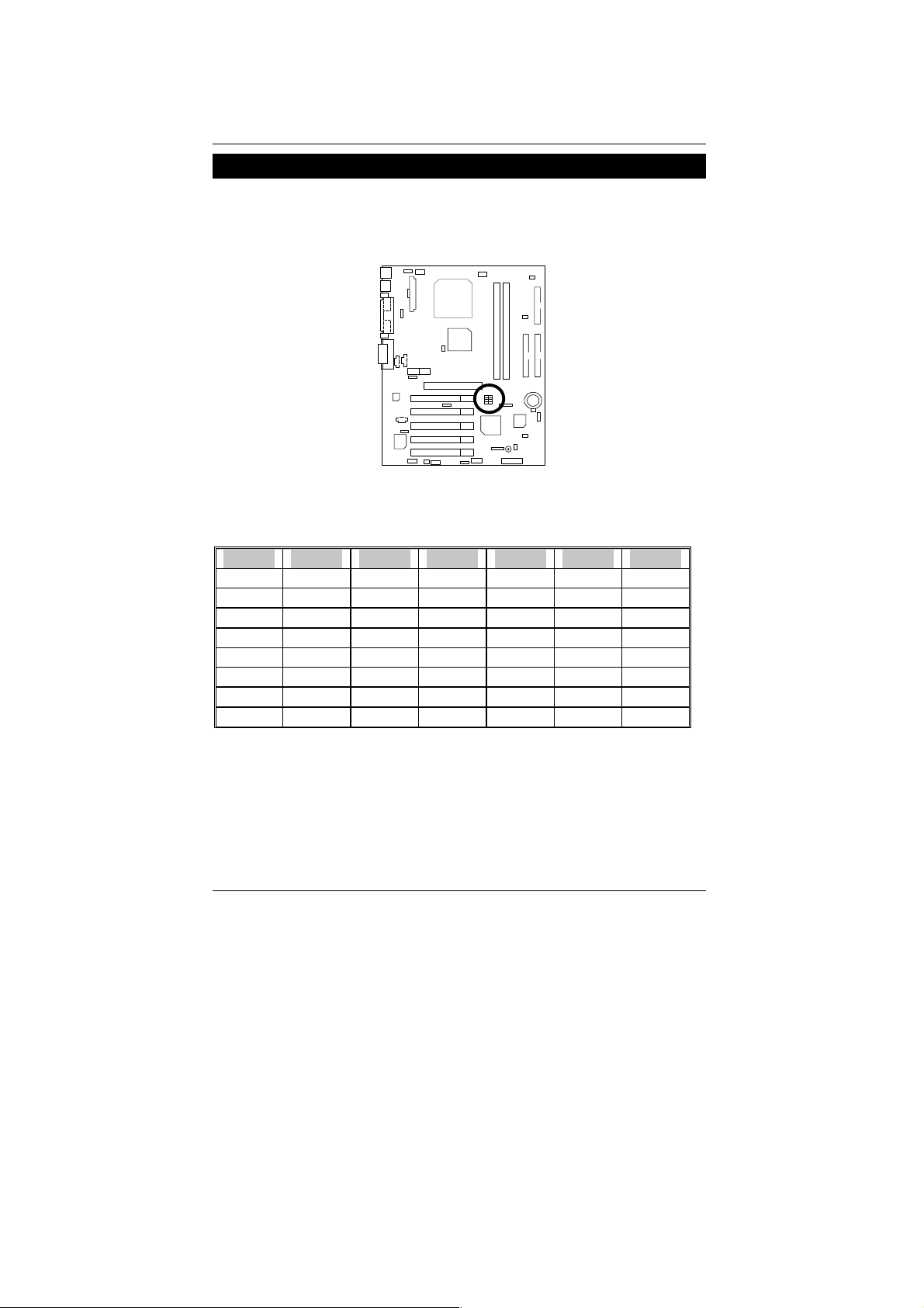
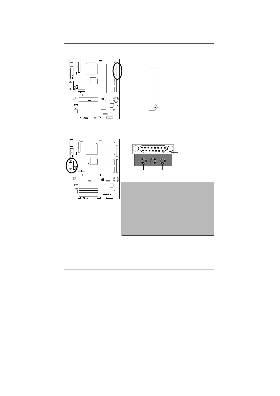
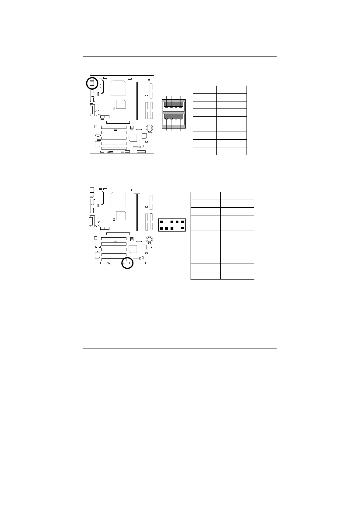
Connectors
ATX Power
COM A / COM B / LPT Port
Connectors
Pin No. Definition
10
15,16,17
GND
3,5,7,13,
1
1,2,11 3.3V
4,6,19,20 VCC
10 +12V
12 -12V
11
20
18 -5V
8 Power Good
9 5V SB (stand by+5V)
14 PS-ON (Soft On/Off)
LPT Port
COM A
COM B
8
Page 16
7DX Motherboard
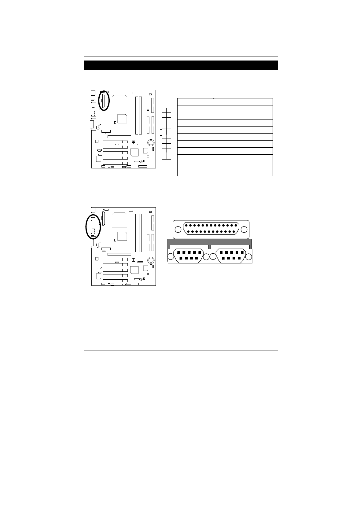
Floppy Connector
Game & Audio Port
FLOPPY1
Red Line
Game
Port
Line Out 1
MIC In
Line In/Line Out 2
Line Out 1: Line Out or SPDIF (The SPDIF output is
capable of providing digital audio to external speakers
or compressed AC3 data to an external Dolby digital
decoder). To enable SPDIF, simply insert SPDIF
connector into Line Out1. Line Out1 will become
SPDIF Out automatically. (see page 35 for more
information).
To enable Four Speaker (for Creative 5880 audio
only), simply follow instructions on page 32 and Line In
will become Line Out2 to support second pair of stereo
speakers.
9
Page 17
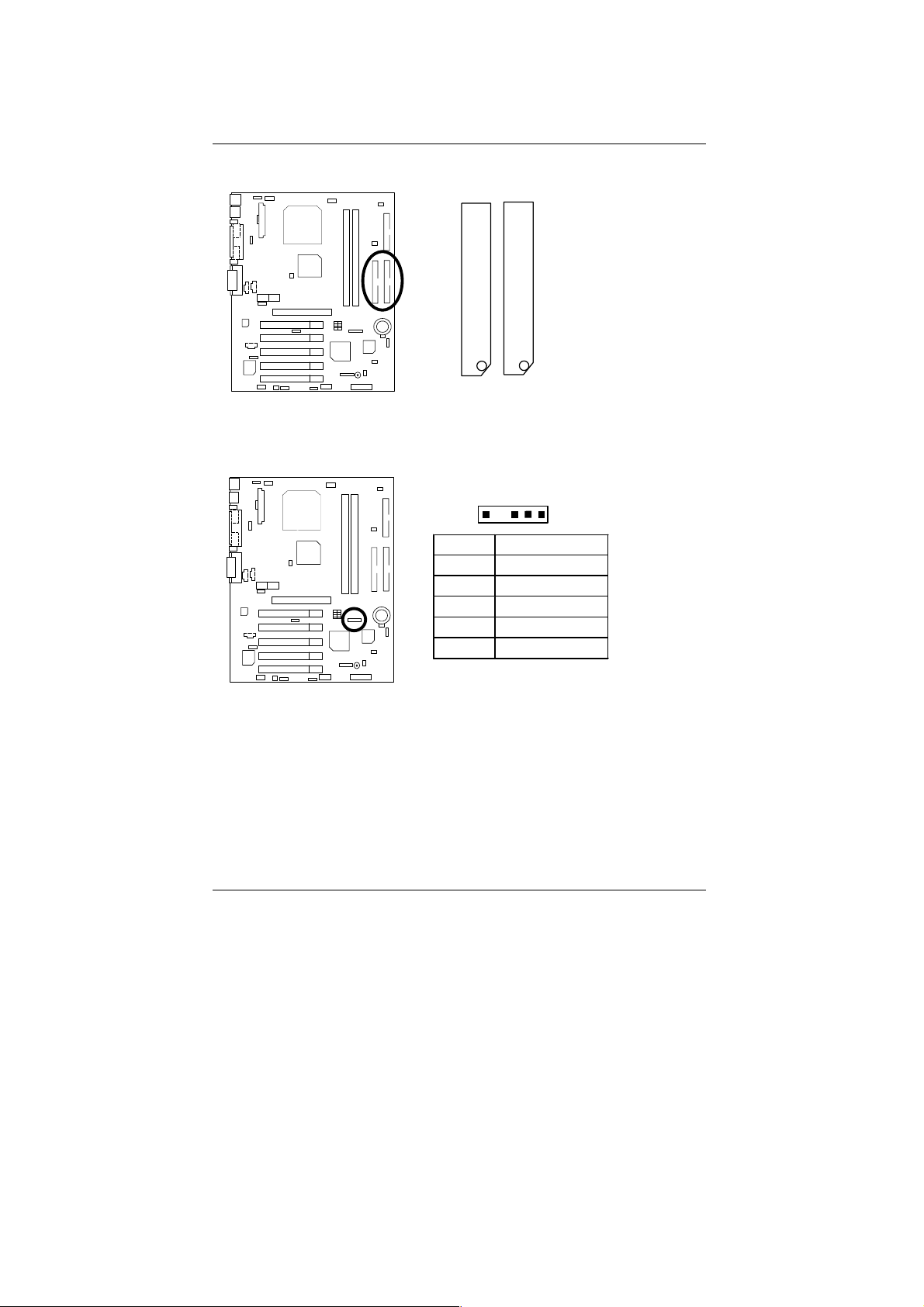
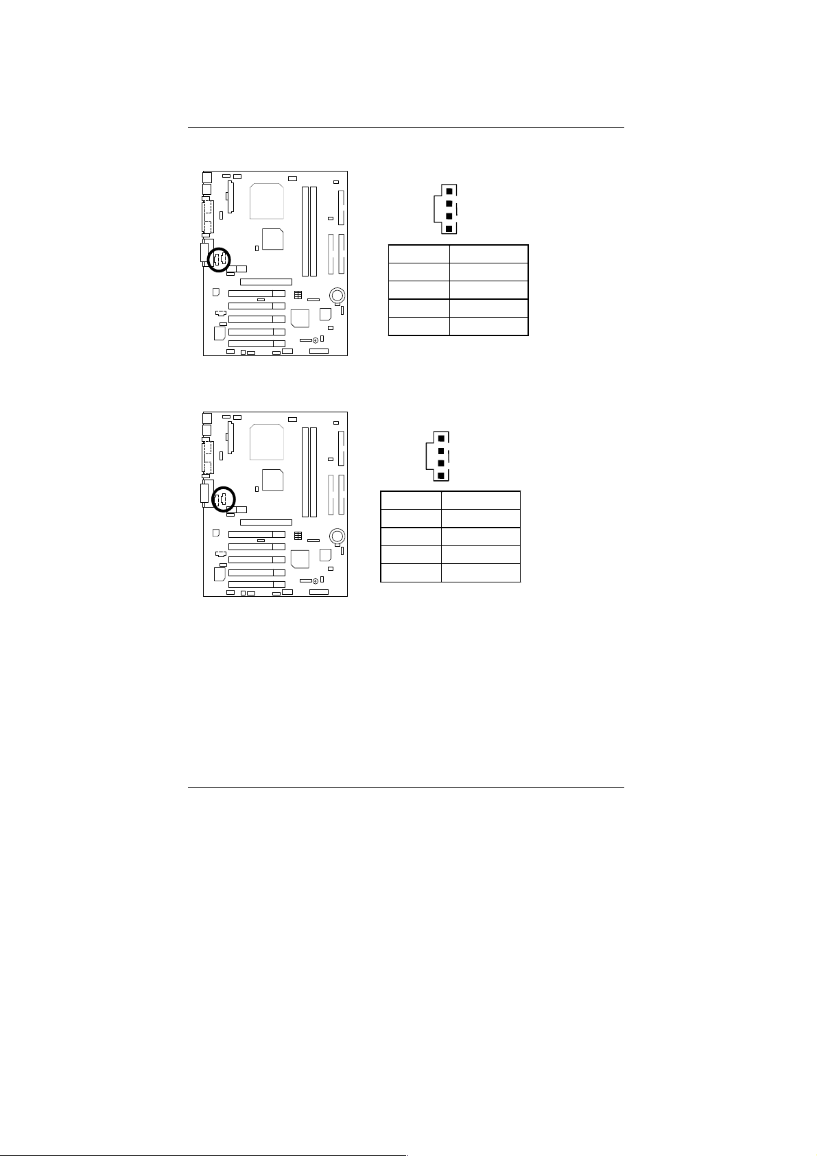
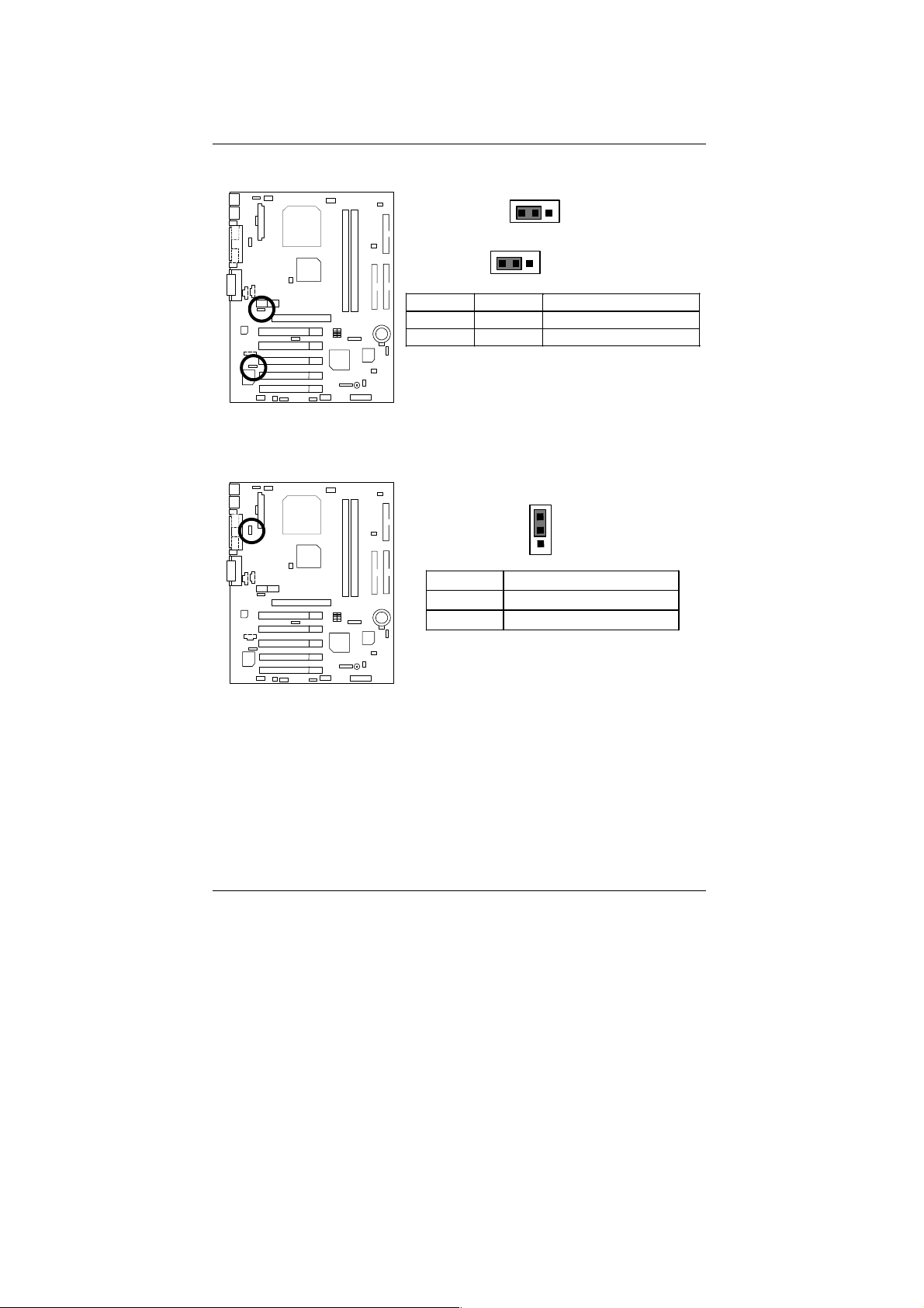
IDE1 (Primary), IDE2 (Secondary) Connector
IDE 1 IDE 2
J1: External SMBUS Header
1
Pin No. Definition
1 SMB CLK
2 NC
3 GND
4 SMB DATA
5 +5V
Connectors
Red Line
10
Page 18
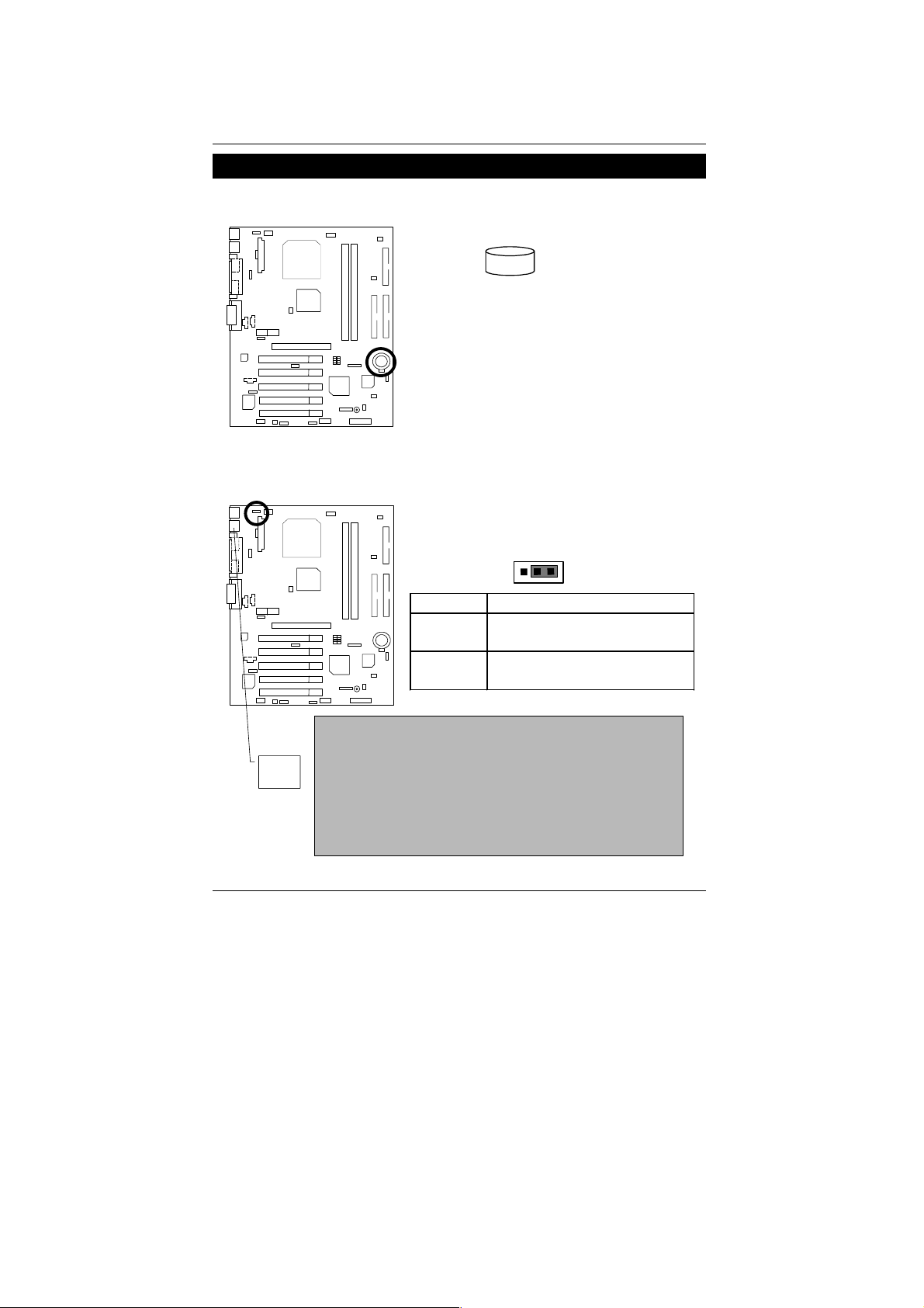
7DX Motherboard
J9: Ring Power On (Internal Modem Card Wake Up)
1
Pin No . Definition
1 Signal
2 GND
J10: Wake On LAN
1
Pin No . D efin ition
1 +5V SB
2 GND
3 Signal
11
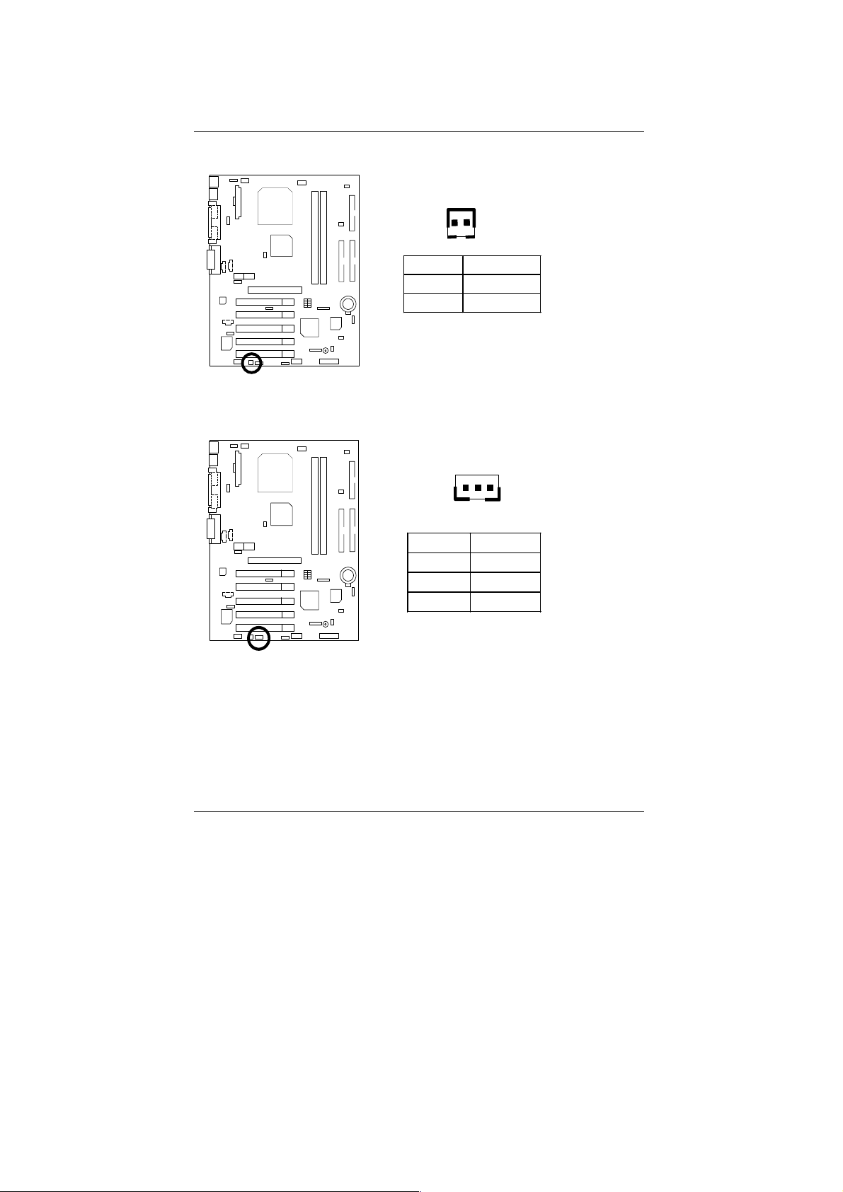
Page 19
J12: IR Header
J15: Power Fan
Connectors
1
Pin No. Definition
1 VCC (+5V)
2 NC
3 IR Data Input
4 GND
5 IR Data Output
1
Pin No . Definition
1 Control
2 +12V
3 NC
12
Page 20
7DX Motherboard
J16: System Fan
J17: CPU Fan
1
Pin No. Definition
1 Control
2 +12V
3 SENSE
1
Pin No. Definition
1 Control
2 +12V
3 SENSE
13
Page 21
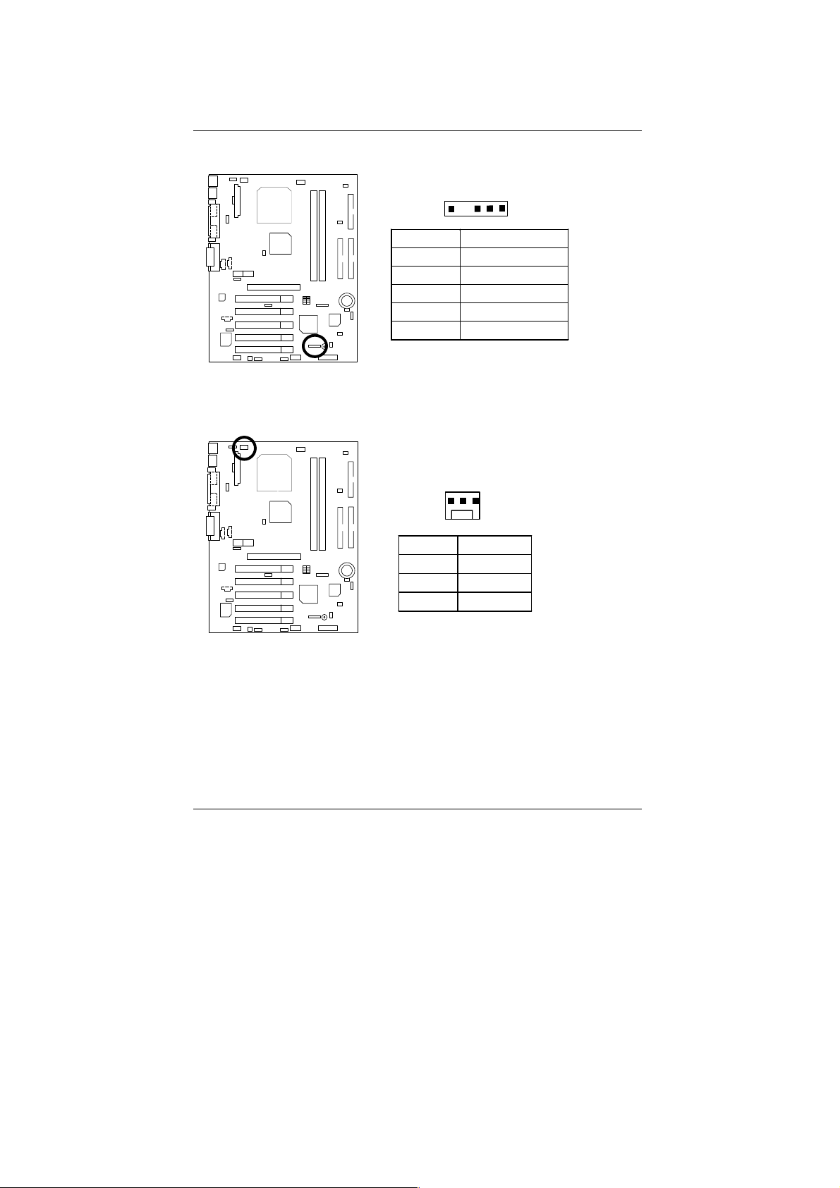
Connectors
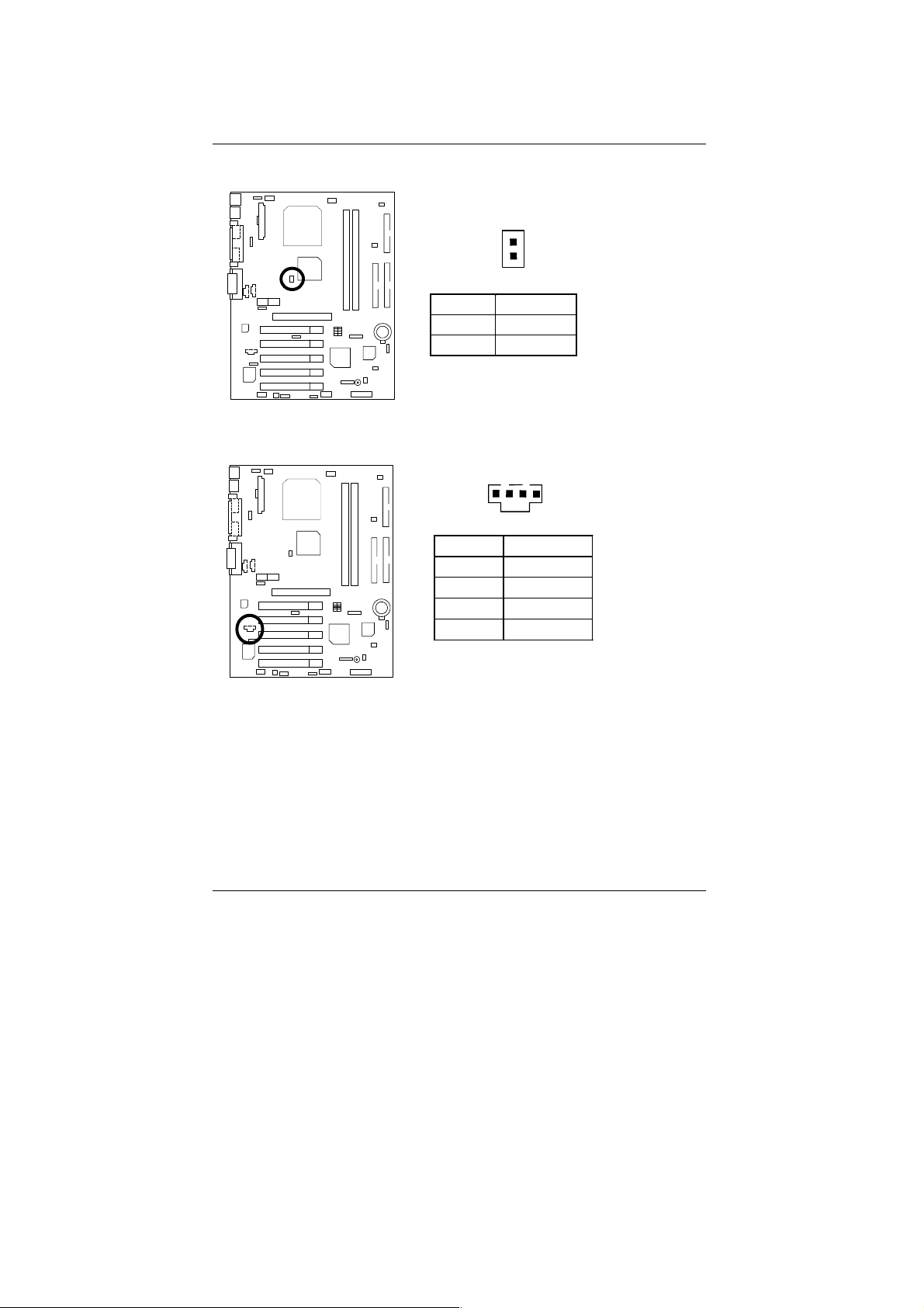
J21: Chip Fan
1
Pin No. Definition
1 GND
2 +12V
J23 TEL: This connector is for Modem with internal voice connector
1
Pin No. Definition
1 Signal-In
2 GND
3 GND
4 Signal-Out
14
Page 22
7DX Motherboard
J24: CD Audio Line In
J25: AUX_IN
1
Pin No. Definition
1 CD-L
2 GND
3 GND
4 CD-R
1
Pin No. Definition
1 AUX-L
2 GND
3 GND
4 AUX-R
15
Page 23
LED2: DIMM LED
DIMM LED
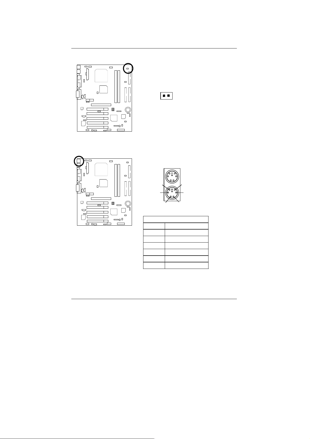
PS/2 Keyboard & PS/2 Mouse Port
Connectors
+
PS/2 Mouse
6
4
2
5
3
1
PS/2 Keyboard
PS/2 Mouse/ Keyboard
Pin No. Definition
1 Data
2 NC
3 GND
4 VCC(+5V)
5 Clock
6 NC
16
Page 24
7DX Motherboard
USB1: Rear USB Port
USB 2: Front USB Connector
2
1
31
24
Pin No. Definition
7
5
1 USB V1
2 USB V0
3 USB D14 USB D05 USB D1+
6
8
6 USB D0+
7 GND
8 GND
Pin No. Definition
1 +5V
10
2 GND
3 USB D24 NC
9
5 USB D2+
6 USB D3+
7 NC
8 USB D39 GND
10 +5V
17
Page 25
Panel and Jumper Definition
Panel And Jumper Definition
BA T1: Batt er y
+
CAUTION
Danger of explosion if battery
is incorrectly replaced.
Replace only with the same or
equivalent type recommended
by the manufacturer.
Dispose of used batteries
acc ording to the manufacturer’s
instructions.
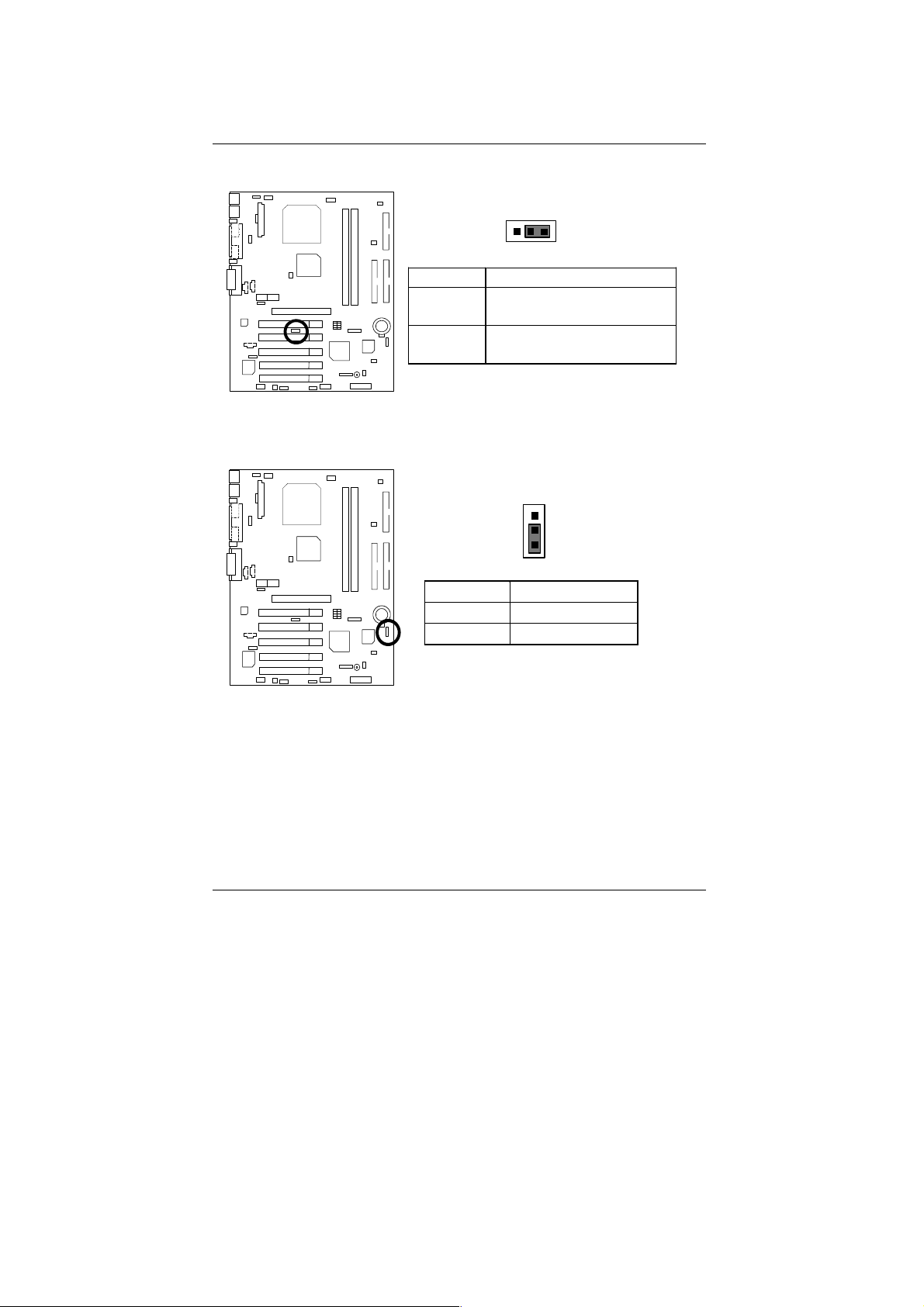
J6: Rear USB Device Wake up Selection (USB Connector USB1)
1
Pin No. Definition
1-2 close Rear USB Device Wake up
Enable
2-3 close Rear USB Device Wake up
Disable (Default)
USB1
(If you want to use “
have to set the BIOS setting “USB Dev Wakeup from S3-S5”
enabled, and the jumper “
*(Power on the computer and as soon as memory counting
starts, press <Del>. You will enter BIOS Setup. Select the
item “
POWER MANAGEMENT SETUP
Dev Wakeup from S3-S5: Enabled
the setting by pressing "ESC" and choose the “SAVE & EXIT
SETUP” option.)
USB Dev Wakeup from S3-S5
” enabled).
J6&J18
”, then select “
”. Remember to save
” function, you
USB
18
Page 26
7DX Motherboard
J7: BIOS Write Protect Function
1
Pin No. Definition
Close Write Prote ct Enab le
Open Write Protect Disable
(Default)
Please set Jumper J7 to “Open”
to enabled BIOS write function when
you update new BIOS or new device.
J8: Front Panel USB Device Wake up Selection (USB Port USB2)
USB2
1
Pin No. Definition
1-2 close
2-3 close
(If you want to use “
have to set the BIOS setting “USB Dev Wakeup From S3-S5”
enabled, and the jumper “
*(Power on the computer and as soon as memory counting
starts, press <Del>. You will enter BIOS Setup. Select the
item “
POWER MANAGEMENT SETUP
Dev Wakeup from S3-S5: Enabled
the setting by pressing "ESC" and choose the “SAVE & EXIT
SETUP” option.)
USB Dev Wakeup From S3-S5
Enable FP USB Device
Wake up
Disable FP USB Devic e
Wake up (Default)
” enabled).
J8&J18
”, then select “
”. Remember to save
19
” function, you
USB
Page 27
J13: Internal Buzzer Selection
J14: 2x11 Pins Front Panel
Panel and Jumper Definition
1
Pin No. Def inition
Close Internal Buzzer Enable
(Default)
Open Internal Buzzer Disable
−P−P+
P
S P K
RE
1
1
PW
GD
1
GN
HD
1
20
Page 28
7DX Motherboard
GN (Green Switch) Open: Normal Operation
Close: Entering Green Mode
GD (Green LED) Pin 1: LED anode(+)
Pin 2: LED cathode(−)
HD (IDE Hard Disk Active LED) Pin 1: LED anode(+)
Pin 2: LED cathode(−)
SPK (Speaker Connector) Pin 1: VCC(+)
Pin 2- Pin 3: NC
Pin 4: Data(−)
RE (Reset Switch) Open: Normal Operation
Close: Reset Hardware System
P+P−P−(Power LED)
Pin 1: LED anode(+)
Pin 2: LED cathode(−)
Pin 3: LED cathode(−)
PW (Soft Power Connector) Open: Normal Operation
Close: Power On/Off
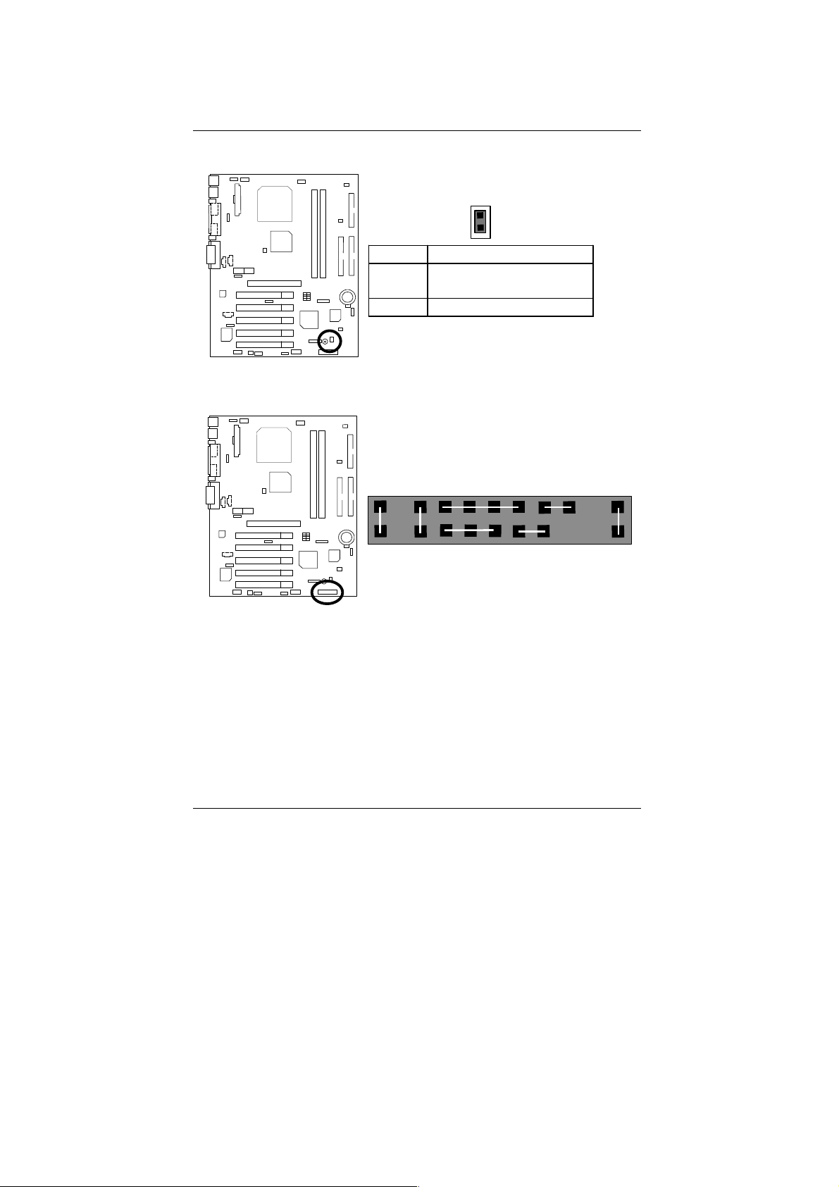
J18: STR Enable/Disable Jumper (Optional)
1
Pin No. Definition
Open STR Disable
Close STR Enable (Default)
21
Page 29
Panel and Jumper Definition
J26 & J27: Primary CODEC Selection (For AC97 Only)
1
J27
J26 J27 Primary CODEC
1-2 close 1-2 close On-board AC97(Default)
2-3 close 2-3 close AMR
J50: S3 KB/MS Wake up (Optional)
Pin No. Definition
1-2 close Normal (Default)
2-3 close S3 KB/MS Wake up
1
J26
1
22
Page 30
7DX Motherboard
JP1: Registered/Unbuffered DDR DIMM Selection (Optional)
1
Pin No. Definition
1-2 close
2-3 close
Support Registered DDR
DIMM
Support Unbuffered DDR
DIMM (Default)
JP5: Clear CMOS Function (Optional)
Pin No. Definition
1-2 Close Normal (Default)
2-3 Close Clear CMOS
1
23
Page 31

Performance List
Performance List
The following performance table lists the results of some popular benchmark testing programs.
These data are provided as reference only and in no way guarantee the system shall perform,
and there is no responsibility for different testing data at exactly the same level. (The different
Hardware & Software con figuration will result in different benchmark testing results.)
• CPU
AMD Althon
1000MHz
• DRAM (64x2) MB DDR (MT8VDDT864AG-2 65A2)
• CACHE SIZE
384 KB integrated in Althon
• DISPLAY GA-GF2000 AGP CARD (32MB)
• STORAGE Onboard IDE (IBM DTLA-307060)
• O.S.
• DRIVER
Windows NT
Display Driver at 1024 x 768 x 16bits colors x 75Hz.
4.0 SPK6
AMD Althon
Processor
1000MHz
(133x7.5)
Winbench99
CPU mark99 95.3
FPU Winmark 99 5490
Business Disk Winmark 99 8890
Hi-End Disk Winmark 99 21500
Business Graphics Winmark 99 558
Hi-End Graphics Winmark 99 1130
Winstone99
Business Winstone99 52.8
Hi-End Winstone99 63.4
24
Page 32

7DX Motherboard
A
Block Diagram
AGPCLK (66MHz)
5 PCI
PCI (33MHz)
AGP
2X/4X
PCI Bus 33MHz
CT5880
Option
AC97
CODEC
AC-Link
MR
AMD-K7
AMD
761
VT82C
686B
Floppy
PS/2
TM
System Bus 100/133MHz
33MHz
LPT Port
CPUCLK (100/133MHz)
100/133MHz
NPCLK (33MHz)
AGPCLK (66MHz)
14.318MHz
2.5V DDR SDRAM
HCLK (100/133MHz)
48MHz
4 USB Ports
Game Port
COM Ports
ATA66/100 IDE
Channels
AGPCLK (66MHz)
PCI (33MHz)
48MHz
14.318MHz
33MHz
ICS
9248-153
25
HCLK (100/133MHz)
NPCLK (33MHz)
AGPCLK (66MHz)
CPUCLK (100/133MHz)
Page 33

Suspend to RAM Installation
Suspend To RAM Installation (Optional)
A.1 Introduce STR function:
Suspend-to-RAM (STR) is a Wi ndows 98 ACPI sleep mode functi on. When recovering from
STR (S3) sleep mode, the system is able to retrieve the last “state” of the system before it
went to sleep and recover to that sta te in just a few sec onds. The “state” i s stored in memory
(RAM) before the system goes to sleep. During STR sleep mode, the system uses only
enough energy to maintain critical information and system functions, primarily the system
state and the ability to recognize various “wake up” triggers or signals, respectively.
A.2 STR function Installation
Please use the following steps to complete the STR function installation.
Step-By-Step Setup
Step 1:
To utilize the STR functio n, the system must be in Windows 98 ACPI mode.
Putting Windows 98 into ACPI mode is fairly easy.
Setup with Windows 98 CD:
A. Insert the Windows 98 CD into your CD-ROM drive, select Start, and then Run.
B. Type (without quotes) “D:\setup” in the window provided. Hit the enter key or click OK.
C. After setup completes, remove the CD, and reboot your system
(This manual assumes that your CD-ROM device drive letter is D:).
26
Page 34

7DX Motherboard
Step 2:
(If you want to use STR Function, please set jumper J18 Closed.)
1
Pin No. Definition
Open STR Disable
Close STR Enable (Default)
Step 3:
Power on the computer and as soon as memory counting starts, press <Del>. You will enter
BIOS Setup. Select the item “POWER MANAGEMENT SETUP”, then select “ACPI Sleep
Type
: S3 (STR)”. Remember t o save the settings by p ressing "ESC" and c hoose the “SAVE
& EXIT SETUP” option.
Congratulation! You have completed the installation and now can use the STR function.
27
Page 35

Suspend to RAM Installation
A.3 How to put your system into STR mode?
There are two ways to accomplish this:
1. Choose the “Stand by” item in the “Shut Down Windows” area.
A. Press the “Start” button and then select “Shut Down”
B. Choose the “Stand by” item and press “OK”
28
Page 36

7DX Motherboard
2. Define the system ”power on” button to initiate STR sleep mode:
A. Double click “My Computer” and then “Control Panel”
B. Double click the “ Power Management” item.
29
Page 37

Suspend to RAM Installation
C. Select the “Advanced” tab and “Standby” mode in Power Buttons.
D. Restart your computer to complete setup.
Now when you want to enter STR sleep mode, just momentarily press the “Power on”
button.
A.4 How to recover from the STR sleep mode?
There are six ways to “wake up” the system:
1. Press the “Power On” button.
2. Use the “Resume by Alarm” function.
3. Use the “Modem Ring On” function.
4. Use the “Wake On LAN” function.
5. Use the “USB Device Wake Up” function.
6. Use the “KB/MS Wake up from S3” function. (Optional)
30
Page 38

7DX Motherboard
A.5 Notices:
1. In order for STR to function prop erly, several ha rdware and software requirements must
be satisfied:
A. Your ATX power s upply must comply with the ATX 2.01 specifi cation (provide more
than 720 mA 5V Stand-By current).
B. Your DDR SDRAM must be DDR-200 or DDR-266 compliant.
2. The DIMM LED will be illuminate d when your system has po wer for memory.
+
DIMM LED
31
Page 39

Four Speaker & SPDIF Introduction
Four Speaker & SPDIF Introduction (Optional)
Four Speaker Introduction
A. What is Four Speaker?
The Creative CT5880 audio chip can support up to 4 speaker output. If you select “Four
speaker out”, Line In will be reconfigured as another line out to support a second pair of
speakers.
B. How to use Four Speaker?
Microsoft Windows 98 Second Edition setup procedure:
a. Click the audio icon along the task bar and select “Configure 3D Audio”
b. Select two speaker (Default)
32
Page 40

7DX Motherboard
c. Select “Four speaker” item.
Microsoft Windows Me setup procedure:
a. Go to “Control Panel”
Double click “Sounds and Multimedia”.
33
Page 41

b. Select “Audio” Page, and click “Advanced” button.
c. Select “Quadraphonic Speakers” and click ok.
Four Speaker & SPDIF Introduction
Click ”Advanced”.
Click “Quadraphonic Speakers”.
C. Four Speaker Application
The four speaker function will only be supported in application softwares that use Microsoft
DirectX and Creative EAX, for example, the game titles, software DVD player and MP3 player.
34
Page 42

7DX Motherboard
SPDIF Introduction
What is SPDIF?
A.
The SPDIF output is capable of providing digi tal audio to external speakers or compressed
AC3 data to an external Dolby digital decoder.
B. How to use SPDIF ?
a. Click your mouse right button in “My Computer” and select the “Properties” item.
b. Click “Device Manager” item.
35
Page 43

Four Speaker & SPDIF Introduction
c. Click “Sound, video and game controllers” item and select the “Creative Sound Blaster
PCI128” item.
d. Click “Settings” item and select the “Output Mode” item.
36
Page 44

7DX Motherboard
e. Click “Digital” item, Line Out will be reconfigure to SPDIF Out.
f. Recommend you to select “Autosense”, It will automatically detect the ty pe (mono or st ereo)
of the audio connector that you plug into Line Out audio jack, the n configure Line Out to
either SPDIF or Speaker accordingly.
37
Page 45

DDR Introduction
DDR Introduction
Established on the existing SDRAM industry infrastructure, DDR (Double Data Rate)
memory is a high performance and cost-effective solution that allows easy adoption for
memory vendors, OEMs and system integrators.
DDR memory is a sensible evolutionary solution for the PC industry that builds on the
existing SDRAM infrastructure, yet makes awesome advances in solving the system
performance bottleneck by doubling the memory bandwidth. DDR SDRAM will offer a
superior solution and migration path from existing SDRAM designs due to its
availability, pricing and overall market support. PC2100 DDR memory (DDR266)
doubles the data rate through reading and writing at both the rising and falling edge of
the clock, achieving data bandwidth 2X greater than PC133 when running with the
same DRAM clock frequency. With peak bandwidth of 2.1GB per second, DDR
memory enables system OEMs to build high performance and low latency DRAM
subsystems that are suitable for servers, workstations, high-end PC’s and value
desktop SMA systems. With a core voltage of only 2.5 Volts compared to conventional
SDRAM's 3.3 volts, DDR memory is a compelling solution for small form factor
desktops and notebook applications.
38
Page 46

7DX Motherboard
@BIOSTM Introduction
Gigabyte announces @BIOS™
Windows BIOS live update utility
Have you ever updated BIOS by yourself? Or
like many other people, you just know what
BIOS is, but always hesitate to update it?
Because you think updating newest BIOS is
unnecessary and actually you don’t know how
to update it.
Maybe not like others, you are very experienced in BIOS updating and spend quite
a lot of time to do it. But of course you don’t like to do it too much. First, download
different BIOS from website and then switch the operating system to DOS mode.
Secondly, use different flash utility to update BIOS. The above process is not a
interesting job. Besides, always be carefully to store the BIOS source code correctly in
your disks as if you update the wrong BIOS, it will be a nightmare.
Certainly, you wonder why motherboard vendors could not just do something right
to save your time and effort and save you from the lousy BIOS updating work? Here it
comes! Now Gigabyte announces @BIOS
This is a smart BIOS update software. It could help you to download the BIOS from
internet and update it. Not like the other BIOS update software, it’s a Windows utility.
With the help of “@BIOS
™
’, BIOS updating is no more than a click.
Besides, no matter which mainboard you are using, if it’s a Gigabyte’s product*,
™
@BIOS
help you to maintain the BIOS. This utility could detect your correct
mainboard model and help you to choose the BIOS accordingly. It then downloads the
BIOS from the nearest Gigabyte ftp site automatically. There are several different
choices; you could use “Internet Update” to download and update your BIOS directly.
Or you may want to keep a backup for your current BIOS, just choose “Save Current
BIOS” to save it first. You make a wise choice to use Gigabyte, and @BIOS
your BIOS smartly. You are now worry free from updating wrong BIOS, and capable to
maintain and manage your BIOS easily. Again, Gigabyte’s innovative product erects a
milestone in mainboard industries.
For such a wonderful software, how much it costs? Impossible! It’s free! Now, if you
buy a Gigabyte’s motherboard, you could find this amazing software in the attached
driver CD. But please remember, connected to internet at first, then you could have a
internet BIOS update from your Gigabyte @BIOS
™
--the first Windows BIOS live update utility.
™
update
™
.
39
Page 47

EasyTuneIII
TM
Introduction
EasyTuneIII
TM
Introduction
Gigabyte announces EasyTuneIII™
Windows overdrive utility
“Overdrive” might be one of the most
common issues in computer field. But have
many users ever tried it? The answer is
probably “no”. Because “overdrive” is thought to
be very difficult and includes a lot of technical
know-how, sometimes “overdrive” is even
considered as special skills found only in some
enthusiasts.
But as to the experts in “overdrive”, what’s the truth? They may spend quite a lot
of time and money to study, try and use many different hardware and software tools
to do “overdrive”. And even with these technologies, they still learn that it’s quite a
risk because the safety and stability of an “overdrive“ system is unknown.
Now everything is different because of a Windows overdrive utility
EasyTuneIII
rule of “overdrive”. This is the first overdrive utility suitable for both normal and power
users. Users can choose either “Easy Mode” or “Advanced Mode” to run “overdrive”
at their convenience. For users who choose “Easy Mode”, they just need to click
“Auto Optimize” to have auto and immediate CPU overclocking. This software will
then overdrive CPU speed automatically with the result being shown in the control
panel. If someone prefers to “overdrive” by oneself, there is also another choice.
Click “Advanced Mode” to enjoy “sport drive” class overclocking. In “Advanced
Mode”, one can change the system bus speed in small increments to get ultimate
system performance. And no matter which mainboard is used, if it’s a Gigabyte’s
product*, EasyTuneIII
Besides, different from other traditional over-clocking methods, EasyTuneIII
doesn’t require users to change neither BIOS nor hardware switch/ jumper setting;
on the other hand, they can do “overdrive” at only one click. Therefore, this is a safer
way for “overdrive” as nothing is changed on software or hardware. If user runs
EasyTuneIII
again and the side effect is then well controlled. Moreover, if one well-performed
system speed been tested in EasyTuneIII™, user can “Save” this bus speed and
“Load” it in next time. Obviously, Gigabyte EasyTuneIII
“overdrive” technology toward to a newer generation.
™
--announced by Gigabyte. This utility has totally changed the gaming
™
helps to perform the best of system.
™
over system’s limitation, the biggest lost is only to restart the computer
40
™
has already turned the
™
Page 48

7DX Motherboard
This wonderful software is now free bundled in Gigabyte motherboard attached
driver CD. Users may make a test drive of “EasyTuneIII
features by themselves.
™
” to find out more amazing
For further technical information, please link to: http://www.gigabyte.com.tw
Note: If your TUCD version is 1.6 or below, please visit our website and
download the latest EasyTuneIII
TM
version.
41
Page 49

Memory Installation
Memory Installation
The motherboard has 2 dual inline memory module (DIMM) sockets. The BIOS will automatically
detects memory type and size. To install the memory module, just push it vertically into the
DIMM Slot .The DIMM module can only fit in one direction due to the notch. Memory size can
vary between sockets.
Total Memory Sizes With Registered DDR DIMM
Devices used on DIMM
64 Mbit
(4Mx4x4 banks)
64 Mbit
(2Mx8x4 banks)
64 Mbit
(1Mx16x4 banks)
128 Mbit
(8Mx4x4 banks)
128 Mbit
(4Mx8x4 banks)
128 Mbit
(2Mx16x4 banks)
256 Mbit
(16Mx4x4 banks)
256 Mbit
(8Mx8x4 banks)
256 Mbit
(4Mx16x4 banks)
512 Mbit
(32Mx4x4 banks)
512 Mbit
(16Mx8x4 banks)
512 Mbit
(8Mx16x4 banks)
1 DIMM
(2Rows)
x64/x72
256 MBytes 512 MBytes
128 MBytes 256 MBytes
64 MBytes 128 MBytes
512 MBytes 1 GBytes
256 MBytes 512 MBytes
128 MBytes 256 MBytes
1 GBytes 2 GBytes
512 MBytes 1 GBytes
256 MBytes 512 MBytes
2 GBytes 4 GBytes
1 GBytes 2 GBytes
512 MBytes 1 GBytes
2 DIMMs
(2Rows each)
x64/x72
42
Page 50

7DX Motherboard
Total Memory Sizes With Unbuffered DDR DIMM
1 DIMM
Devices used on DIMM
64 Mbit
(2Mx8x4 banks)
64 Mbit
(1Mx16x4 banks)
128 Mbit
(4Mx8x4 banks)
128 Mbit
(2Mx16x4 banks)
256 Mbit
(8Mx8x4 banks)
256 Mbit
(4Mx16x4 banks)
512 Mbit
(16Mx8x4 banks)
512 Mbit
(8Mx16x4 banks)
(2Rows)
x64/x72
128 MBytes 256 MBytes
64 MBytes 128 MBytes
256 MBytes 512 MBytes
128 MBytes 256 MBytes
512 MBytes 1 GBytes
256 MBytes 512 MBytes
1 GBytes 2 GBytes
512 MBytes 1 GBytes
2 DIMMs
(2Rows each)
x64/x72
43
Page 51

BIOS Setup
Page Index for BIOS Setup Page
The Main Menu P.46
Standard CMOS Features P.49
Advanced BIOS Features P.53
Advanced Chipset Features P.55
Integrated Peripherals P.59
Power Management Setup P.64
PnP / PCI Configurations P.68
PC Health Status P.70
Frequency / Voltage Control P.72
Load Fail-Safe Defaults P.74
Load Optimized Defaults P.75
Set Supervisor / User Password P.76
Save & Exit Setup P.77
EXIT Without Saving P.78
44
Page 52

7DX Motherboard
BIOS Setup
BIOS Setup is an overview of the BIOS Setup Interface. The interface allows users to modify the
basic system configuration, which is stored in battery-backed CMOS RAM so that the Setup
information can be retained when the power is turned off.
ENTERING SETUP
Power ON the computer and press <Del> immediately will allow you to enter Setup. If
unsuccessful, you can restart the system and try again by pressing the "RESET" bottom on the
system case. You may also restart by simultaneously pressing <Ctrl> − <Alt>− <Del> keys.
CONTROL KEYS
<↑> Move to previous item
<↓> Move to next item
<←> Move to the item in the left hand
<→> Move to the item in the right hand
<Esc> Main Menu - Quit and not save changes into CMOS
Status Page Setup Menu and Option Page Setup Menu - Exit current page
and return to Main Menu
<+/PgUp> Increase the numeric value or make changes
<-/PgDn> Decrease the numeric value or make changes
<F1> General hel p, only for Status Page Setup Menu and Option Page Setup
Menu
<F2> Reserved
<F3> Reserved
<F4> Reserved
<F5> Restore the previous CMOS value from CMOS, only for Option Page
Setup Menu
<F6> Load the default CMOS value from BIOS default table, only for Optio n
Page Setup Menu
<F7>
<F8> Reserved
<F9> Reserved
<F10> Save all the CMOS changes, only for Main Menu
Load the Optimized Defaults
45
Page 53

BIOS Setup
GETTING HELP
Main Menu
The on-line description of the highlighted setup function is displayed at the bottom of the screen.
Status Page Set up Menu / Option Page Setup Menu
Press F1 to pop up a small hel p window that describes the appropriate keys to use and the
possible selections for the highlighted item. To exit the Help Window press <Esc>.
The Main Menu
Once you enter Award BIOS CMOS Setup Utility, the Main Menu (Figure 1) will appear on the
screen. The Main Menu allows you to select from nine setup functions and two exit choices. Use
arrow keys to select among the items and press <Enter> to accept or enter the sub-menu.
CMOS Setup Utility-Copyright( C ) 1984-2000 Award Software
Standard CMOS Features
4
Advanced BIOS Features Load Fail-Safe Defaults
4
Advanced Chipset Features Load Optimized Defaults
4
Integrated Peripherals Set Supervisor Password
4
Power Management Setup Set User Password
4
PnP/PCI Configurations Save & Exit Setup
4
PC Health Status Exit Without Saving
4
ESC:Quit
F10:Save & Exit Setup
Time, Date, Hard Disk Type…
Figure 1: Main Menu
Frequency/Voltage Control
4
: Select Item
↑↓→ ←
46
Page 54

7DX Motherboard
•••• Standard CMOS Features
This setup page includes all the adjustable items in standard compatible BIOS.
•••• Advanced BIOS Features
This setup page includes all the adjustable items of Award special enhanced features.
•••• Advanced Chipset Features
This setup page includes all the adjustable items of chipset special features.
•••• Integrated Peripherals
This setup page includes all onboard peripherals.
•••• Power Management Setup
This setup page includes all the adjustable items of Green function features.
•••• PnP/PCI Configurations
This setup page includes all the adjustable configurations of PCI & PnP ISA resources.
•••• PC Health Status
This setup page is for monitoring system status such as temperature, voltage, and fan
speed.
•••• Frequency/Voltage Control
This setup page is for controlling CPU clock and frequency ratio.
•••• Load Fail-Safe Defaults
Load Fail-Safe Defaults option loads preset system parameter values to set the system in
its most stable configurations.
•••• Load Optimized Defaults
Load Optimized Defaults option loads preset system parameter values to set the system in
its highest performance configurations.
•••• Set Supervisor Password
Set Change or disable password. It allows you to limit access to the system and/or BIOS
setup.
47
Page 55

•••• Set User Password
Set Change or disable password. It allows you to limit access to the system.
•••• Save & Exit Setup
Save CMOS value settings to CMOS and exit setup.
•••• Exit Without Saving
Abandon all CMOS value changes and exit setup.
BIOS Setup
48
Page 56

7DX Motherboard
Standard CMOS Features
The items in Standard CMOS Setup Menu (Figure 2) are divided into 9 categories. Each
category includes none, on e or m ore than one s etup it ems. Us e the a rrow s to highl ight the item
and then use the <PgUp> or <PgDn> keys to select the value in each item.
CMOS Setup Utility-Copyright( C ) 1984-2000 Award Software
Date (mm:dd:yy) Mon , Feb 21 2000 Item Help
Time (hh:mm:ss) 2 : 31 : 24
IDE Primary Master None
4
IDE Primary Slave None
4
IDE Secondary Master None
4
IDE Secondary Slave None
4
century
Drive A 1.44M, 3.5 in.
Drive B None
Floppy 3 Mode Support Disabled
Video EGA / VGA
Halt On All, But Keyboard
Base Memory Size 640K
Extended Memory Size 63488K
Total Memory 64512K
Standard CMOS Features
Menu Level 4
Change the
Day, month,
Year and
:Move Enter:Select +/-/ P U/PD:Value F10:Save ESC:Exit F 1:G ener al Help
↑↓→ ←
F5:Previous Values F6:Fail-Safe Defaults F7:Optimized Defaults
Figure 2: Standard CMOS Features
•••• Date
The date format is <week>, <month> <day> <year>.
Week The week, from Sun to Sat, determined by the BIOS and is display-only
Month The month, Jan. Through Dec.
Day The day, from 1 to 31 (or the maximum allowed in the month)
Year The year, from 1994 through 2079
49
Page 57

BIOS Setup
•••• Time
The times format in <hour> <minute> <second>. The time is calculated based on the
24-hour military-time clock. For example, 1 p.m. is 13:00:00.
•••• IDE Primary Master / Slave, Secondary Master / Slave
The category identifies the type of hard disk from drive C to F that has been installed in the
computer. There are two settings: Auto, and Manual. Ma nual: HDD ty pe is user-d efinable;
Auto will automatically detect HDD type.
Note that the specifications of your drive must match with the drive table. The hard disk will
not work properly if you enter improper information for this category.
If you select User Type, related information will be asked to enter to the following items.
Enter the information directly from the keyboard and press <Enter>. Such information
should be provided in the documentation form your hard disk vendor or the system
manufacturer.
CYLS. Number of cylinders
HEADS number of heads
PRECOMP write precomp
LANDZONE Landing zone
SECTORS number of sectors
If a hard disk has not been installed select NONE and press <Enter>.
•••• Drive A / Drive B
The category identifies the ty pe of floppy disk drive A or dri ve B that has been install ed in
the computer.
None No floppy drive installed
360K, 5.25 in. 5.25 inch PC-type standard drive; 360K byte capacity.
1.2M, 5.25 in. 5.25 inch AT-type high-density drive; 1.2M byte capac ity (3.5 inch
when 3 Mode is Enabled).
720K, 3.5 in. 3.5 inch double-sided drive; 720K byte capacity
1.44M, 3.5 in. 3.5 inch double-sided drive; 1.44M byte capacity.
2.88M, 3.5 in. 3.5 inch double-sided drive; 2.88M byte capacity.
50
Page 58

7DX Motherboard
•••• Floppy 3 Mode Support (for Japan Area)
Disabled Normal Floppy Drive. (Default value)
Drive A Drive A is 3 mode Floppy Drive.
Drive B Drive B is 3 mode Floppy Drive.
Both Drive A & B are 3 mode Floppy Drives.
•••• Video
The category detects the type of adapter used for the primary system monitor, which must
match your video display card and moni tor. Although secondary monitors are s upported,
you do not have to select the type in setup.
EGA/VGA Enhanced Graphics Adapter/Video Graphics Array. For EGA, VGA,
SVGA, or PGA monitor adapters
CGA 40 Color Graphics Adapter, power up in 40 column mode
CGA 80 Color Graphics Adapter, power up in 80 column mode
MONO Monochrome adapter, includes high resolution monochrome adapters
•••• Halt on
The category determines whether the computer will stop if an error is detected during
power up.
NO Errors The system boot will not stop for any error that may be detected.
All Errors The system boot will stop on any error detected.
All, But Keyboard The system boot will not stop for a keyboard error; it will stop for
all other errors. (Default value)
All, But Diskette The system boot will not stop for a disk error; it will stop for all
other errors.
All, But Disk/Key The system boot will not stop for a keyboard or disk error; it will
stop for all other errors.
51
Page 59

BIOS Setup
•••• Memory
The category is display -only which is determined by POST (Power On Self Test) of the
BIOS.
Base Memory Size
The POST of the BIOS will determine the amount of base (or conventional)
memory installed in the system.
640 K for systems with 640 K or more memory installed on the motherboard.
Extended Memory Size
The BIOS determines how much extended memory is present during the POST.
This is the amount of memory located above 1 MB in the CPU's memory
address map.
52
Page 60

7DX Motherboard
Advanced BIOS Features
CMOS Setup Utility-Copyright( C ) 1984-2000 Award Software
Advanced BIOS Features
Virus Warning Disabled Item Help
First Boot Device Floppy
Second Boot Device IDE-0
Third Boot Device CDROM
Floppy Drive Seek Disabled
BootUp Num-Lock On
Password Check Setup
HDD S.M.A.R.T Capabil i ty Disabled
Menu Level 4
Allows you to
choose the VIRUS
Warning feature
For IDE Hard disk
Boot sector
Protection. If this
Function is enable
And someone
Attempt to write
Data into this area
, BIOS will show
A warning
Message on
Screen and alarm
beep
:Move Enter:Select +/-/PU/PD:Value F10:Save ESC:Exit F1:General Help
↑↓→ ←
F5:Previous Values F6:Fail-Safe Defaults F7:Optimized Defaults
Figure 3: Advanced BIOS Features
•••• Virus Warning
If it is set to enable, a warning will be displayed on the screen when there is any attempt to
write to the boot sector or partition table of the hard disk drive. The system will halt and the
following error message will appear in the mean time. You can run anti-virus program to
locate the problem.
Enabled Activates virus protection and displays a warning message whenever
anything attempts to write to the boot sector or the hard disk partition
table.
Disabled No warning message appears when anything attempts to write to the
boot sector or hard disk partition table. (Default value)
53
Page 61

BIOS Setup
First / Second / Third Boot device
••••
Floppy Set your boot device priority to Floppy.
LS120 Set your boot device priority to LS120.
IDE-0~3 Set your boot device priority to IDE-0~3.
SCSI Set your boot device priority to SCSI.
CDROM Set your boot device priority to CDROM.
ZIP Set your boot device priority to ZIP.
Disabled Disable this function.
LAN Set your boot device priority to LAN.
• Floppy Drive Seek
During POST, BIOS will determine if the floppy disk drive installed is 40 or 80 tracks. 360
type is 40 tracks while 720, 1.2 and 1.44 are all 80 tracks.
Enabled BIOS searches for floppy disk drive to determine if it is 40 or 80
tracks. Note that BIOS can not differentiate between 720, 1.2 or 1.44
drive type as they are all 80 tracks.
Disabled BIOS will not se arch for the type of floppy disk drive by track number.
Note that there will not be any warning message if the drive installed
is 360. (Default Value)
BootUp Num-Lock
••••
On Keypad is number keys. (Default value)
Off Keypad is arrow keys.
•••• Password Check
This category allows you to limit access to the system and Setup, or just to Setup.
System The user must enter correct password in or der to access the system
and/or BIOS Setup.
Setup The user must enter correct password in order to access the system.
(Default value)
HDD S.M.A.R.T. Capability
••••
Enabled Enable HDD S.M.A.R.T. Capability.
Disabled Disable HDD S.M.A.R.T. Capability. (Default value)
54
Page 62

7DX Motherboard
Advanced Chipset Features
CMOS Setup Utility-Copyright( C ) 1984-2000 Award Software
Advanced Chipset Features
AGP Aperture Size 64 Item Help
AGP Fast Write Enabled
AGP Mode 4X
AGP Always Compensate Enabled
SDRAM ECC Setting Disabled
DRAM Timing setting by Auto
X DRAM PH Limit 8 Cycle
X DRAM Idle Limit 8 Cycle
X DRAM Trc Timing Value 8 Cycle
X DRAM Trp Timing Value 3 Cycle
X DRAM Tras Timing Value 7 Cycle
X DRAM CAS Latency 2 Cycle
X SDRAM Trcd Timing Value 3 Cycle
:Move Enter:Select +/-/PU/PD:Value F10:Save ESC:Exit F1:General Help
↑↓→ ←
F5:Previous Values F6:Fail-Safe Defaults F7:Optimized Defaults
Menu Level 4
Figure 4: Advanced Chipset Features
•••• AGP Aperture Size
32MB Set AGP Aperture Size to 32MB.
64MB Set AGP Aperture Size to 64MB. (Default Value)
128MB Set AGP Aperture Size to 128MB.
256MB Set AGP Aperture Size to 256MB.
•••• AGP Fast Write
Enabled Enable AGP Fast Write function. (Default Value)
Disabled Disable this function.
•••• AGP Mode
4X Set AGP Mode to 4X. (Default Value)
1X/2X Set AGP Mode to 1X/2X.
55
Page 63

BIOS Setup
•••• AGP Always Compensate
Enabled Enable AGP Always Compensate function. (Default Value)
Disabled Disable this function.
•••• SDRAM ECC Setting
Disabled Disable DRAM ECC Setting function. (Default Value)
Check Only
Correct Error
Correct + Scrub
Set DRAM ECC Setting to Check Only. Enable DRAM error
checking function.
Set DRAM ECC Setting to Correct Errors. Enable DRAM 1 bit
error checking and correcting in CPU/AGP/PCI.
Set DRAM ECC Setting to Correct+S crub. Enable DRAM 1bi t erro r
checking and correcting in CPU/AGP/PCI and DRAM.
•••• DRAM Timing setting by
Auto Set DRAM Timing setting to Auto. (Default value)
Manual Set DRAM Timing setting to Manual.
•••• DRAM P H Limit
This function specify the number of consecutive Page-Hit requests to allow before
choosing a non-Page-Hit request.
1 Cycle Set DRAM PH Limit to 1 Cycle.
4 Cycle Set DRAM PH Limit to 4 Cycle.
8 Cycle Set DRAM PH Limit to 8 Cycle.
16 Cycle Set DRAM PH Limit to 16 Cycle.
•••• DRAM Idle Limit
This function specify the number of idle cycles to wait before precharging an idle bank.(Idle
cycles are defined as cycles where no valid request is asserted to the MCT.)
0 Cycle Set DRAM Idle Limit to 0 Cycle.
8 Cycle Set DRAM Idle Limit to 8 Cycle.
12 Cycle Set DRAM Idle Limit to 12 Cycle.
16 Cycle Set DRAM Idle Limit to 16 Cycle.
24 Cycle Set DRAM Idle Limit to 24 Cycle.
32 Cycle Set DRAM Idle Limit to 32 Cycle.
48 Cycle Set DRAM Idle Limit to 48 Cycle.
Disabled Disable this function.
56
Page 64

7DX Motherboard
•••• DRAM Trc Timing Value
This function specify the minimum time from activate to activate of the same bank.
3 Cycle Set DRAM Trc Timing Value to 3 Cycle.
4 Cycle Set DRAM Trc Timing Value to 4 Cycle.
5 Cycle Set DRAM Trc Timing Value to 5 Cycle.
6 Cycle Set DRAM Trc Timing Value to 6 Cycle.
7 Cycle Set DRAM Trc Timing Value to 7 Cycle.
8 Cycle Set DRAM Trc Timing Value to 8 Cycle.
9 Cycle Set DRAM Trc Timing Value to 9 Cycle.
10 Cycle Set DRAM Trc Timing Value to 10 Cycle.
•••• DRAM Trp Timing Value
This function specify the delay from precharge command to activate command.
1 Cycle Set DRAM Trp Timing Value to 1 Cycle.
2 Cycle Set DRAM Trp Timing Value to 2 Cycle.
3 Cycle Set DRAM Trp Timing Value to 3 Cycle.
4 Cycle Set DRAM Trp Timing Value to 4 Cycle.
•••• DRAM Tras Timing Value
This function specifies the minimum bank (active time: time from active to precharge of
same bank).
2 Cycle Set DRAM Tras Timing Value to 2 Cycle.
3 Cycle Set DRAM Tras Timing Value to 3 Cycle.
4 Cycle Set DRAM Tras Timing Value to 4 Cycle.
5 Cycle Set DRAM Tras Timing Value to 5 Cycle.
6 Cycle Set DRAM Tras Timing Value to 6 Cycle.
7 Cycle Set DRAM Tras Timing Value to 7 Cycle.
8 Cycle Set DRAM Tras Timing Value to 8 Cycle.
9 Cycle Set DRAM Tras Timing Value to 9 Cycle.
•••• DRAM CAS Latency
This function specify the DRAM CAS Latency.
2 Cycle Set DRAM CAS Latency to 2 Cycle.
2.5 Cycle Set DRAM CAS Latency to 2.5 Cycle.
57
Page 65

BIOS Setup
•••• SDRAM Trcd Timing Value
This function specifies the delay from the activation of a bank to the time that a read or
write command is accepted.
1 Cycle Set SDRAM Trcd Timing Value to 1 Cycle.
2 Cycle Set SDRAM Trcd Timing Value to 2 Cycle.
3 Cycle Set SDRAM Trcd Timing Value to 3 Cycle.
4 Cycle Set SDRAM Trcd Timing Value to 4 Cycle.
58
Page 66

7DX Motherboard
Integrated Peripherals
CMOS Setup Utility-Copyright( C ) 1984-2000 Award Software
Integrated Peripherals
OnBoard IDE1 Enabled Item Help
OnBoard IDE2 Enabled
VGA Boot from AGP
OnBoard Sound Chip Enabled
BIOS Flash Protection Disabled
USB Controller 1 Enabled
USB Controller 2 Enabled
USB Legacy Support Disabled
AC97 Audio Auto
AC97 Modem Auto
Onboard FDD Controller Enabled
Onboard Serial Port 1 Auto
Onboard Serial Port 2 Auto
UART 2 Mode Standard
IR Function Duplex Half
TX, RX inverting enable No, Yes
Onboard Parallel Port 378/IRQ7
Onboard Parallel Mode Normal
ECP Mode Use DMA 3
Parallel Port EPP Type EPP1.9
Sound Blaster
♣
SB I/O Base Address
♣
SB IRQ Select
♣
SB DMA Select
♣
MPU-401
♣
MPU-401 I/O Address
♣
Game Port (200-207H)
♣
:Move Enter:Select +/-/ P U/PD:Value F10:Save ESC:Exit F 1:G eneral Help
↑↓→ ←
F5:Previous Values F6:Fail-Safe Defaults F7:Optimized Defaults
Disabled
220H
IRQ 5
DMA 1
Disabled
330-333H
Enabled
Menu Level 4
Figure 5: Integrated Peripherals
This item will only be shown when there is sound chip onboard.
These two items will be available when ”UART 2 Mode” is set to HPSIR or ASKIR.
These two items will be available when ”Onboard Parallel Mode” is set to ECP/EPP.
♣ These seven items will not be shown when there is sound chip onboard.
•••• OnBoard IDE1
Enabled Enable onboard 1st channel IDE port. (Default value)
Disabled Disable onboard 1st channel IDE port.
59
Page 67

•••• OnBoard IDE2
Enabled Enable onboard 2nd channel IDE port. (De fau lt value)
Disabled Disable onboard 2nd channel IDE port.
VGA Boot from
••••
PCI Slot Set VGA Boot from PCI Slot.
AGP Set VGA Boot from AGP. (Default value)
Onboard Sound Chip
•
Enabled Enable Onboard Sound Chip function. (Default Value)
Disabled Disable this function.
BIOS Flash Protection
•
Enabled Enable BIOS Flash Protection.
Disabled Disable BIOS Flash Protection. (Default Value)
•••• USB Controller 1
Enabled Enable USB Controller 1. (Default value)
Disabled Disable USB Controller 1.
•••• USB Controller 2
BIOS Setup
Enabled Enable USB Controller 2. (Default value)
Disabled Disable USB Controller 2.
•••• USB Legacy Support
Enabled Enable USB Device (Such as USB KB, Mouse) support in Legacy Mode,
eg. DOS. Win NT4.0 .
Disabled Disable OnBoard Legacy Audio. (Default Value)
•••• AC97 Audio
Auto BIOS will automatically detect onboard AC97 Audio. (Default value)
Disabled Disable AC97 Audio.
•••• AC97 Modem
Auto Bios will automatically detect onboard AC97 Modem. (Default value)
Disabled Disabled AC97 Modem.
60
Page 68

7DX Motherboard
•••• Onboard FDD Controller
Enabled Enable onboard FDD port. (Default value)
Disabled Disable onboard FDD port.
•••• Onboard Serial Port 1
Auto BIOS will automatically setup the port 1 a ddress. (Default value)
3F8/IRQ4 Enable onboard Serial port 1 and address is 3F8.
2F8/IRQ3 Enable onboard Serial port 1 and address is 2F8.
3E8/IRQ4 Enable onboard Serial port 1 and address is 3E8.
2E8/IRQ3 Enable onboard Serial port 1 and address is 2E8.
Disabled Disable onboard Serial port 1.
•••• Onboard Serial Port 2
Auto BIOS will automatically setup the port 2 address. (Default Value)
3F8/IRQ4 Enable onboard Serial port 2 and address is 3F8.
2F8/IRQ3 Enable onboard Serial port 2 and address is 2F8.
3E8/IRQ4 Enable onboard Serial port 2 and address is 3E8.
2E8/IRQ3 Enable onboard Serial port 2 and address is 2E8.
Disabled Disable onboard Serial port 2.
• UART 2 Mode
Standard Normal Serial port operation. (Default Value)
HPSIR Set onboard I/O chip Serial Port B to HPSIR Mode.
ASKIR Set onboard I/O chip Serial Port B to ASKIR Mode.
• IR Function Duplex
Half
Full
TX, RX inverting enable
••••
No, No Set TX, RX inverting enable to No, No.
No, Yes Set TX, RX inverting enable to No, Yes. (Default value)
Yes, No Set TX, RX inverting enable to Yes, No.
Yes, Yes Set TX, RX inverting enable to Yes, Yes.
Half Duplex IR function. (Default Value)
Full Duplex IR function.
61
Page 69

•••• Onboard Parallel Port
378/IRQ7 Enable onboard LPT port and address is 378/IRQ7. (Default Value)
278/IRQ5 Enable onboard LPT port and address is 278/IRQ5.
Disabled Disable onboard LPT port.
3BC/IRQ7 Enable onboard LPT port and address is 3BC/IRQ7.
•••• Onboard Parallel Mode
Normal Normal Setting. (Default value)
EPP Using Parallel port as Enhanced Parallel Port.
ECP Using Parallel port as Extended Capabilities Port.
ECP/EPP Using Parallel port as ECP & EPP mode.
•••• ECP Mode Use DMA
3 Set ECP Mode Use DMA to 3. (Default Value)
1 Set ECP Mode Use DMA to 1.
•••• Parallel Port EPP Type
EPP 1.9 Set Parallel Port EPP Type to EPP 1.9. (Default value)
EPP 1.7 Set Parallel Port EPP Type to EPP 1.7.
•••• Sound Blaster
Enabled Enable Sound Blaster.
Disabled Disable Sound Blaster. (Default Value)
BIOS Setup
•••• SB I/O Base Address
220H Set SB I/O Base Address to 220H. (Default Value)
240H Set SB I/O Base Address to 240H.
260H Set SB I/O Base Address to 260H.
280H Set SB I/O Base Address to 280H.
•••• SB IRQ Select
IRQ 5 / 10. (Default Value: 5)
•••• SB DMA Select
DMA 0 / 1 / 2 / 3. (Default Value: 1)
62
Page 70

7DX Motherboard
•••• MPU-401
Enabled Enable MPU-401.
Disabled Disable MPU-401. (Default Value)
Ps. When Force Feedback joystick is used, MPU-401 needs to be Enable.
•••• MPU-401 I/O Address
330-333H Set MPU-401 I/O Address to 330-333H. (Default Value)
300-303H Set MPU-401 I/O Address to 300-303H.
310-313H Set MPU-401 I/O Address to 310-313H.
320-323H Set MPU-401 I/O Address to 320-323H.
•••• Game Port (200-207H)
Disabled Disable Game Port (200-207H).
Enabled Enable Game Port (200-207H). (De fa ult Value)
63
Page 71

Power Management Setup
BIOS Setup
CMOS Setup Utility-Copyright( C ) 1984-2000 Award Software
ACPI Sleep Typ e S1(POS) Item Help
Suspend Time Out (Minute) Disabled
Soft-Off by PBTN Instant-off
System aft er AC Back Off
PME Event Wake Up Enabled
USB Dev Wakeup from S3-S5 Disabled
ModemRingOn/WakeOnLan Enabled
MODEM Use IRQ 3
Resume by RTC Alarm Disabled
X Date (of Month) Alarm 0
X Time (hh:mm:ss) Alarm 0 0 0
IRQ Wakeup Events Press Enter
VGA OFF
LPT & COM LPT/COM
HDD & FDD ON
PCI master OFF
:Move Enter:Select +/-/PU/PD:Value F10:Save ESC:Exit F1:General Help
↑↓→ ←
F5:Previous Values F6:Fail-Safe Defaults F7:Optimized Defaults
Power Management Setup
Menu Level 4
Figure 6: Power Management Setup
•••• ACPI Sleep Type
S1 (POS) Set ACPI Sleep Type to S1 (Power On Suspend). (Default value)
S3 (STR) Set ACPI Sleep Type to S3 (Suspend to RAM).
•••• Suspend Time Out (Minute)
Disabled Disable Suspend Time Out Function. (Default Value)
30 Sec - 1 Hour Set the timer to enter Suspend Time Out.
•••• Soft-off by PBTN
Instant-off Soft switch ON/OFF for POWER ON/OFF. (Default value)
Suspend Soft switch to enter Suspend Mode.
64
Page 72

7DX Motherboard
•••• System After AC Back
Last State System power on depends on the status before AC is lost.
Off Always in Off state when AC power returns. (Default value)
On Always power on the system when AC p ower returns.
• PME Event Wake Up
Disabled Disable PME Event Wake Up.
Enabled Enable PME Event Wake Up. (Default Value)
• USB Dev Wakeup from S3-S5
Enabled Enable USB Device Wakeup from ACPI S3, S4 and S5 mode.
Disabled Disable USB Device Wakeup from ACPI S3, S4 and S5 mode.
(Default Value)
•••• ModemRingOn/WakeOnLan
Disabled Disable ModemRingOn/WakeOnLan with #RI.
Enabled Enable ModemRingOn/WakeOnLan with #RI. (Default Value)
•••• MODEM Use IRQ
NA Set MODEM Use IRQ to NA.
3 Set MODEM Use IRQ to 3. (Default value)
4 Set MODEM Use IRQ to 4.
5 Set MODEM Use IRQ to 5.
7 Set MODEM Use IRQ to 7.
9 Set MODEM Use IRQ to 9.
10 Set MODEM Use IRQ to 10.
11 Set MODEM Use IRQ to 11.
•••• Resume by RTC Alarm
You can set “Resume by RTC Alarm” item to Enabled and key in date/time to power on
system.
Disabled Disable this function. (Default value)
Enabled Enable alarm function to POWER ON system or wake up system from
sleep mode.
65
Page 73

If the default value is Enabled.
Date ( of Month) Alarm : 0~31
Time ( hh: mm: ss) Alarm : (0~23) : (0~59) : (0~59)
•••• IRQ Activity
Disabled Disable this function.
Primary The resource is used by Primary device. (Default value)
Secondary The resource is used by Secondary device.
•••• IRQ [3-15]
Disabled Disable specified IRQ to Wake up system from sleep mode or Reload
PM Timer to prevent system to enter sleep mode.
Enabled Enable specified IRQ to Wake up system from sleep mode or Reload
PM Timer to prevent system to enter sleep mode.
•••• VGA
BIOS Setup
OFF
ON
Disable monitor VGA activity to prevent system to enter sleep mode.
(Default value)
Enable monitor VGA activity to prevent system to enter sleep mode.
•••• LPT & COM
LPT/COM Enable LPT/COM Ports Activity to Wake up system from sleep
mode or prevent system to enter sleep mode. (Defau lt valu e)
NONE Normal Operation.
LPT Enable LPT Ports Activity to Wake up system from sleep mode or
prevent system to enter sleep mode.
COM Enable COM Ports Activity to Wake up system from sleep mode or
prevent system to enter sleep mode.
•••• HDD & FDD
ON Enable HDD & FDD Ports Activity to Wake up system from sleep mode
or prevent system to enter sleep mode. (Default value)
OFF Disable HDD & FDD Ports Activity to Wake up system from sleep mode
or prevent system to enter sleep mode.
66
Page 74

7DX Motherboard
•••• PCI master
ON Enable PCI master Activity to Wake up system from sleep mode or
prevent system to enter sleep mode.
OFF Disable PCI master Activity to Wake up system from sleep mode or
prevent system to enter sleep mode. (Default value)
67
Page 75

PnP/PCI Configurations
BIOS Setup
CMOS Setup Utility-Copyright( C ) 1984-2000 Award Software
Reset Configuration Data Disabled Item Help
Resources Controlled By Auto (ESCD)
X IRQ Resources Press Enter
INT A Assignment Auto
INT B Assignment Auto
INT C Assignment Auto
INT D Assignment Auto
Move Enter:Select +/-/PU/PD:Value F10:Save ESC:Exit F1:General Help
↑↓→ ←
F5:Previous Values F6:Fail-Safe Defaults F7:Optimized Defaults
PnP/PCI Configurations
Menu Level 4
Default is Disabled.
Select Enabled to
reset Extended System
Configuration Data
ESCD) when you exit
Setup if you have
installed a new add-on
and the System
reconfiguration has
caused such a serious
conflict that the OS
cannot boot
Figure 7: PnP/PCI Configurations
•••• Reset Configuration Data
Disabled Disable this function. (Default value)
Enabled Enable Reset Configuration Data function.
•••• Resources Controlled by
Manual User can set the PnP resource (I/O Address , IRQ & DMA channels)
used by legacy ISA DEVICE.
Auto(ESCD) BIOS automatically use these PnP rescuers. (Default value)
•••• IRQ (3, 4, 5, 7, 9, 10, 11, 12, 14, 15)
PCI Device The resource is used by PCI device. (Default value)
Reserved Set the resource to reserved.
68
Page 76

7DX Motherboard
•••• INT A / B / C / D Assignment
Auto Will be automatically detected by BIOS. (Default value)
3 Set INT A / B / C / D Assignment to 3.
4 Set INT A / B / C / D Assignment to 4.
5 Set INT A / B / C / D Assignment to 5.
7 Set INT A / B / C / D Assignment to 7.
9 Set INT A / B / C / D Assignment to 9.
10 Set INT A / B / C / D Assignment to 10.
11 Set INT A / B / C / D Assignment to 11.
12 Set INT A / B / C / D Assignment to 12.
14 Set INT A / B / C / D Assignment to 14.
15 Set INT A / B / C / D Assignment to 15.
69
Page 77

PC Health Status
BIOS Setup
CMOS Setup Utility-Copyright( C ) 1984-2000 Award Software
PC Health Status
Shutdown Temperature Disabled Item Help
CPU Warning Temperature Disabled
CPU Fan Warning No
System Fan Warning No
Current CPU Temp.
Current System Temp.
57
31
°
°
C/134°F
C/87°F
CPU Fan Speed 5553 RPM
System Fan Speed 0 RPM
Vcore 3.10V
3.3V 3.31V
5V 5.10V
12V 12.42V
Move Enter:Select +/-/PU/PD:Value F10:Save ESC:Exit F1:General Help
↑↓→ ←
F5:Previous Values F6:Fail-Safe Defaults F7:Optimized Defaults
Menu Level
4
Figure 8: PC Health Status
•••• Shutdown Temperature (°
(This function will be eff ective only for the operating systems that support ACPI Function.)
Disabled Disable ACPI Shutdown function. (Default Value)
60°C / 140°F Monitor CPU Temp. , If Temp. > 60°C / 140°F system will
70°C / 158°F Monitor CPU Temp. , If Temp. > 70°C / 158°F system will
80°C / 176°F Monitor CPU Temp. , If Temp. > 80°C / 176°F system will
90°C / 194°F Monitor CPU Temp. , If Temp. > 90°C / 194°F system will
°C / °°°°F)
°°
automatically power off.
automatically power off.
automatically power off.
automatically power off.
70
Page 78

7DX Motherboard
•••• CPU Warning Temperature (°
60°C / 140°F Monitor CPU Temp. at 60°C / 140°F.
70°C / 158°F Monitor CPU Temp. at 70°C / 158°F.
80°C / 176°F Monitor CPU Temp. at 80°C / 176°F.
90°C / 194°F Monitor CPU Temp. at 90°C / 194°F.
Disabled Disable this function. (Default value)
°C / °°°°F)
°°
•••• CPU Fan Warning
No Disable this function. (Default value)
Yes Enable CPU Fan Warning function to display warning message
when CPU Fan speed is under lower limit RPM.
•••• System Fan Warning
No Disable this function. (Default value)
Yes Enable System Fan Warning function to display warning
message when System Fan speed is under a lower limit RPM.
•••• CPU Temp. (°
Detect CPU Temperature automatically.
•••• System Temp. (°
Detect System Temperature automatically.
°C / °°°°F)
°°
°C / °°°°F)
°°
•••• CPU Fan / System Fan Speed (RPM)
Detect Fan speed status automatically.
•••• Current Voltage (V) Vcore / 3.3V / 5V / 12V
Detect system’s voltage status automatically.
71
Page 79

Frequency/Voltage Control
BIOS Setup
CMOS Setup Utility-Copyright( C ) 1984-2000 Award Software
Frequency/Voltage Control
ClkGen Spread Spectrum Enabled Item Help
CPU Host/PCI Clock Default
Move Enter:Select +/-/PU/PD:Value F10:Save ESC:Exit F1:General Help
↑↓→ ←
F5:Previous Values F6:Fail-Safe Defaults F7:Optimized Defaults
Menu Level
4
Figure 9: Frequency/Voltage Control
•••• ClkGen Spread Spectrum
Disabled Disable this function.
Enabled Enable Clock Generator Spread Spectrum function to improve
CE/FCC. (Default value)
•••• CPU Host/PCI Clock
The table below is shown only when CPU DIP switch setting is below 133MHz:
Default When CPU Host/PCI Clock setting is set to Default, the clock will
depend on DIP switch setting. (Default value)
100/33Mhz Set CPU Host/PCI Clock to 100/33Mhz.
102/34Mhz Set CPU Host/PCI Clock to 102/34Mhz.
104/35Mhz Set CPU Host/PCI Clock to 104/35Mhz.
108/36Mhz Set CPU Host/PCI Clock to 108/36Mhz.
112/38Mhz Set CPU Host/PCI Clock to 112/38Mhz.
116/39Mhz Set CPU Host/PCI Clock to 116/39Mhz.
118/40Mhz Set CPU Host/PCI Clock to 118/40Mhz.
72
Page 80

7DX Motherboard
The table below is shown only when CPU DIP switch setting is 133MHz or above:
Default When CPU Host/PCI Clock setting is set to Default, the clock will
depend on DIP switch setting. (Default value)
133/33Mhz Set CPU Host/PCI Clock to 133/33Mhz.
134/34Mhz Set CPU Host/PCI Clock to 134/34Mhz.
135/34Mhz Set CPU Host/PCI Clock to 135/34Mhz.
137/34Mhz Set CPU Host/PCI Clock to 137/34Mhz.
139/35Mhz Set CPU Host/PCI Clock to 139/35Mhz.
143/36Mhz Set CPU Host/PCI Clock to 143/36Mhz.
145/37Mhz Set CPU Host/PCI Clock to 145/37Mhz.
149/38Mhz Set CPU Host/PCI Clock to 149/38Mhz.
73
Page 81

Load Fail-Safe Defaults
BIOS Setup
CMOS Setup Utility-Copyright( C ) 1984-2000 Award Software
Standard CMOS Features
4
Advanced BIOS Features Load Fail - Safe Defaults
4
Advanced Chipset Features Load Optimized Defaults
4
Integrated Peripherals Set Supervisor Password
4
Power Management Setup Set User Password
4
PnP/PCI Confi gurations Save & Exit Setup
4
PC Health Status Exit Without Saving
4
ESC:Quit
F10:Save & Exit Setup
Load Fail-Safe Defaults (Y/N)? N
Load Fail-Safe Defaults
Figure 10: Load Fail-Safe Defaults
Frequency/Voltage Control
4
: Select Item
↑↓→ ←
•••• Load Fail-Safe Defaults
Fail−Safe defaults contain the most appropriate system parameter values of to configure
the system to achieve maximum stability.
74
Page 82

7DX Motherboard
Load Optimized Defaults
CMOS Setup Utility-Copyright( C ) 1984-2000 Award Software
Standard CMOS Features
4
Advanced BIOS Features Load Fail-Safe Defaults
4
Advanced Chipset Features Load Optimized Defaults
4
Integrated Peripherals Set Supervisor Password
4
Power Management Setup Set User Password
4
PnP/PCI Configurations Save & Exit Setup
4
PC Health Status Exit Without Saving
4
ESC:Quit
F10:Save & Exit Setup
Load Optimized Defaults (Y/N)? N
Load Optimized Defaults
Figure 11: Load Optimized Defaults
Frequency/Voltage Control
4
: Select Item
↑↓→ ←
•••• Load Optimized Defaults
Optimized defaults contain the most appropriate system paramete r values to configur e the
system to achieve maximum performance.
75
Page 83

BIOS Setup
Set Supervisor / User Password
When you select this function, the following message will appear at the center of the screen to
assist you in creating a password.
CMOS Setup Utility-Copyright( C ) 1984-2000 Award Software
Standard CMOS Features
4
Advanced BIOS Features
4
Advanced Chipset Features Load Optimized Defaults
4
Integrated Peripherals
4
Power Management Setup Set User Password
4
Frequency/Voltage Control
4
Load Fail-Safe Defaults
Set Supervisor Password
Enter Password:
PnP/PCI Configurations Save & Exit Setup
4
PC Health Status Exit Without Saving
4
ESC:Quit
F10:Save & Exit Setup
Change / Set / Disable Password
Figure 12: Password Setting
Type the password, up to eight characters, and press <Enter>. You will be asked to confirm the
password. Type the password again and press <Enter>. You may also press <Esc> to abort the
selection and not enter a password.
To disable password, just press <Enter> when you a re prompt ed to enter password. A message
“PASSWORD DISABLED” will appear to confirm the password being disabled. Once the
password is disabled, the system will boot and you can enter Setup freely.
The BIOS Setup program allows you to specify two separate passwords: a SUPERVISOR
PASSWORD and a USER PASSWORD. When disabled, anyone may access all BIOS Setup
program function. When enabled, the Supervisor password is required for entering the BIOS
Setup program and having full configuration fields, the User password is required to access only
basic items.
If you select “System” at “Password Check” in Advanced BIOS Feature Menu, you will be
prompted for the password every time the system is rebooted or any time you try to enter Setup
Menu.
If you select “Setup” at “ Password Check” in Advanced BIOS Feature Menu, you will be
prompted only when you try to enter Setup.
↑↓→ ←
: Select Item
76
Page 84

7DX Motherboard
Save & Exit Setup
CMOS Setup Utility-Copyright( C ) 1984-2000 Award Software
Standard CMOS Features
4
Advanced BIOS Features Load Fail-Safe Defaults
4
Advanced Chipset Features Load Optimized Defaults
4
Integrated Peripherals Set Supervisor Password
4
Power Management Setup Set User Password
4
PnP/PCI Configuratio ns Save & Exit Setup
4
PC Health Status Exit Without Saving
4
ESC:Quit
F10:Save & Exit Setup
Type "Y" will quit the Setup Utility and save the user setup value to RTC CMOS.
Type "N" will return to Setup Utility.
SAVE to CMOS and EXIT (Y/N)? Y
Save Data to CMOS
Figure 13: Save & Exit Setup
Frequency/Voltage Control
4
: Select Item
↑↓→ ←
77
Page 85

Exit Without Saving
BIOS Setup
CMOS Setup Utility-Copyright( C ) 1984-2000 Award Software
Standard CMOS Features
4
Advanced BIOS Features Load Fail-Safe Defaults
4
Advanced Chipset Features Load Optimized Defaults
4
Integrated Peripherals Set Supervisor Password
4
Power Management Setup Set User Password
4
PnP/PCI Configurations Save & Exit Setup
4
PC Health Status Exit Without Saving
4
ESC:Quit
F10:Save & Exit Setup
Quit Without Saving (Y/N)? N
Abandon all Datas
Frequency/Voltage Control
4
: Select Item
↑↓→ ←
Figure 14: Exit Without Saving
Type "Y" will quit the Setup Utility without saving to RTC CMOS.
Type "N" will return to Setup Utility.
78
Page 86

7DX Motherboard
Appendix
Appendix A: AMD 761_VIA 686A/B Chipsets Driver Installation
A.AMD AGP Miniport Driver (Win98/SE/ME only):
Insert the support CD that came with your motherboard into your CD-ROM driver or
double –click the CD driver icon in My Computer to bring up the screen.
2.Click “Next”.
1.Click “AMD AGP Miniport Driver”
item.
(1)
When the AMD AGP Miniport Driver
installation is completed, please restart your
computer.
(2)
(4)
3.Click “Finish”.
(3)
79
Page 87

Appendix
B: VIA IDE Bus Master Driver Installation
Insert the support CD that came with your motherboard into your CD-ROM drive or double-click
the CD drive icon in My Computer to bring up the setup screen.
1.Click “VIA IDE Bus Master
Driver” item.
(1)
3.Click ”Next”.
(3)
2.Click ”Next”.
(2)
4.Click ”Next”.
(4)
5.Click ”Next”.
6.Click ”Next”.
(5)
80
(6)
Page 88

7DX Motherboard
7.Click “Finish” to
restart computer.
(7)
(8)
81
Page 89

Appendix B: Creative Sound Driver Installation (Optional)
Insert the support CD that came with your motherboard into your CD-ROM driver or
double –click the CD driver icon in My Computer to bring up the screen.
Press “Audio” icon.
Appendix
1.Click “Creative CT5880
Sound Driver”.
(1)
3.Click “Yes”.
(3)
5.Click “Next”.
2.Click “OK”.
(2)
4.Click “Next”.
(4)
6.Click here.
(5)
(6)
82
Page 90

7DX Motherboard
7.Click “Next”.
(7)
(8)
8.Click “Finish” to
restart computer.
(9)
83
Page 91

Appendix C: EasyTuneIII Setup
Insert the support CD that came with your motherboard into your CD-ROM driver or
double –click the CD driver icon in My Computer to bring up the screen.
Press “tool” icon.
1.Click “EasyTune III Setup”
item.
Appendix
(1)
2.Click “Next”.
(3)
4.Click “Next”.
(5)
(2)
3. Please enter your name and
company name, then click “Next”.
(4)
5. Click “Next”.
(6)
84
Page 92

7DX Motherboard
6.Click “Finish” to
restart computer.
(7)
(8)
85
Page 93

Appendix
Appendix D: BIOS Flash Procedure
BIOS update procedure:
If your OS is Win9X, we recommend that you used Gigabyte @BIOSTM Program to flash BIOS.
Click “Tool”.
Click “@BIOS Writer v1.05a”.
Click “”.
Methods and steps:
I. Update BIOS through Internet
a.Click "Internet Update" icon
b.Click "Update New BIOS" icon
c.
Select @BIOS
@BIOS
soon)
d. Select the exact model name on your motherboard
e. System will automatically download and update the BIOS.
TM
TM
sever ( "Gigabyte @BIOSTM sever 1 in Taiwan" and "Gigabyte
sever 2 in Taiwan" are available for now, the others will be completed
Click Here.
86
Page 94

7DX Motherboard
II. Update BIOS NOT through Internet:
a.Do not click "Internet Update" icon
b.Click "Update New BIOS"
c. Please select "All Files" in dialog box while opening the old file.
d. Please search for BIOS unzip file, downloading from internet or any other methods
III. Save BIOS
IV. Check out supported motherboard and Flash ROM:
Note:
(such as: 7DX.F1).
e. Complete update process following the instruction.
In the very beginning, there is "Save Current BIOS" icon shown in dialog box. It
means to save the current BIOS version.
In the very beginning, there is "About this program" icon shown in dialog box. It can
help you check out which kind of motherboard and which brand of Flash ROM are
supported.
a.In method I, if it shows two or more motherboard's model names to be selected,
please make sure your motherboard's model name again. Sellecting name will
cause the system unbooted.
b.In method II, be sure that motherboard's model name in BIOS unzip file are the
same as your motherboard's. Otherwise, your system won't boot.
c. In method I, if the BIOS file you need cannot be found in @BIOS server, please go
onto Gigabyte's web site for downloading and updating it according to method II.
d. Please note that any intercorruption during updating will cause system unbooted
87
Page 95

Appendix
Or else you can select flash BIOS in DOS mode.
Please check your BIOS vendor (AMI or AWARD), your motherboard name and PCB
version on the motherboard.
1. Format a bootable system floppy diskette by the command “format a:/s” in command
mode.
2. Visit the Gigabyte website at http:// www.gigabyte.com.tw
, Select the BIOS file you
need and download it to your bootable floppy diskette.
3. Insert the bootable diskette containing the BIOS file into the floppy diskette driver.
4. Assuming that the floppy diskette driver is A, reboot the system by using the A: driver.
At the A: > prompt, run the BIOS upgraded file by executing the Flash BIOS utility
and the BIOS file with its appropriate extension.
Example: (AMI tool)
(Where 7dx.f1 is name of the BIO S file name)
A:>flashxxx.exe 7dx.f1
Example: (Award tool) (Where 7dx.f1 is name of the BIOS file name)
A:>Awdflash.exe 7dx.f1
5. Upon pressing the <Enter> key, a flash memory writer menu will appear on screen.
Enter the new BIOS file name with its extension filename into the text box after file
name to program.
6. If you want to save the old BIOS file(perform as soon as system is operational, this is
recommended), select Y to DO YOU WANT TO SAVE BIOS, then type the old BIOS
filename and the extension after filename to save: This option allows you to copy the
contents of the flash memory chip onto a diskette, giving you a backup copy of the
original motherboard BIOS in case you need to re-install it. Select N to DO YOU
WANT TO SAVE BIOS, if you don’t want to save the old BIOS file.
7. After the decision to save the old BIOS file or not is made, select Y to ARE YOU
SURE TO PROGRAM when the next menu appear; wait until a message showing
Power Off or Reset the system appears. Then turn off your system.
8. Remove the diskette and restart your system.
9. Hold down <Delete> key to enter BIOS setup. You must select “Load Setup BIOS
Default” to activate the new BIOS, then you may set other item from the main menu.
88
Page 96

7DX Motherboard
Appendix E: Acronyms
Acronyms Meaning
ACPI Advanced Configuration and Power Interface
APM Advanced Power Management
AGP Accelerated Graphics Port
AMR Audio Modem Riser
ACR Advanced Communications Riser
BIOS Basic Input / Output System
CPU Central Processing Unit
CMOS Complementary Metal Oxide Semiconductor
CRIMM Continuity RIMM
CNR Communication and Netwo rki ng Rise r
DMA Direct Memory Access
DMI Desktop Management Interface
DIMM Dual Inline Memory Module
DRM Dual Retention Mechanism
DRAM Dynamic Random Access Memory
DDR Double Data Rate
ECP Extended Capabilities Port
ESCD Extended System Configuration Data
ECC Error Checking and Correcting
EMC Electromagnetic Compatibility
EPP Enhanced Parallel Port
ESD Electrostatic Discharge
FDD Floppy Disk Device
FSB Front Side Bus
HDD Hard Disk Device
IDE Integrated Dual Channel Enhanced
IRQ Interrupt Request
I/O Input / Output
IOAPIC Input Output Advanced Programmable Input Controller
ISA Industry Standard Architecture
LAN Local Area Network
LBA Logical Block Addressing
LED Light Emitting Diode
MHz Megahertz
MIDI Musical Interface Digital Interface
MTH Memory Translator Hub
MPT Memory Protocol Translator
NIC Network Interface Card
OS Operating System
To be continued…
89
Page 97

Acronyms Meaning
OEM Original Equipment Manufacturer
PAC PCI A.G.P. Controller
POST Power-On Self Test
PCI Peripheral Component Interconnect
RIMM Rambus in-line Memory Module
SCI Special Circumstance Instructions
SECC Single Edge Contact Cartridge
SRAM Static Random Access Memory
SMP Symmetric Multi-Processing
SMI System Management Interrupt
USB Universal Serial Bus
VID Voltage ID
Appendix
90
 Loading...