

Page 1

查询DS42514供应商
DS42514
Stacked Multi-Chip Package (MCP) Flash Memory and SRAM
Am29DL163D Bottom Boot 16 Megabit (2 M x 8-Bit/1 M x 16-Bit) CMOS 3.0 V o lt-only,
Simultaneous Operation Flash Memory and 4 Mbit (512 K x 8-Bit/ 256 K x 16-Bit) Static RAM
DISTINCTIVE CHARACTERISTICS
MCP Features
■ Power supply voltage of 2.7 to 3.3 volt
■ High performance
— 85 ns maximum access time
■ Package
— 69-Ball FBGA
■ Operating Temperature
— –25°C to +85°C
Flash Memory Features
ARCHITECTURAL ADVANTAGES
■ Simultaneous Read/Write oper at io ns
— Data can be continuously read from one bank while
executing erase/program functions in other bank
— Zero latency between read and write operations
■ Secured Silicon (SecSi) Sector: Extra 64 KByte sector
— Factory locked and identifiable: 16 bytes available for
secure, random factory Electronic Serial Number; verifiable
as factory locked through autoselect function.
— Customer lockable: Can be read, programmed, or erased
just like other sectors. Once locked, data cannot be changed
■ Zero Power Operation
— Sophisticated power management circuits reduce power
consumed during inactive periods to nearly zero
■ Bottom boot block
■ Manufactured on 0.23 µm process technology
■ Compatible with JEDEC standards
— Pinout and software compatible with single-power-supply
flash standard
PERFORMANCE CHARACTERISTICS
■ High performance
— 85 ns access time
— Program time: 7 µs/word typical utilizing Accelerate function
■ Ultra low power consump tion (typical values)
— 2 mA active read current at 1 MHz
— 10 mA active read current at 5 MHz
— 200 nA in standby or automatic sleep mode
■ Minimum 1 mill i on write cycl es guaranteed per sector
■ 20 Year data retention at 125°C
— Reliable operation for the life of the system
SOFTWARE FEATURES
■ Data Management Software (DMS)
— AMD-supplied software manages data programming and
erasing, enabling EEPROM emulation
— Eases sector erase limitations
■ Supports Common Flash Memory Interface (CFI)
■ Erase Suspend/Erase Resume
— Suspends erase operations to allow programming in same
bank
■ Data# Polling and Toggle Bits
— Provides a software method of detecting the status of
program or erase cycles
■ Unlock Bypass Program command
— Reduces overall programming time when issuing multiple
program command sequences
HARDWARE FEATURES
■ Any combination of sectors can be erased
■ Ready/Busy# output (RY/BY#)
— Hardware method for detecting program or erase cycle
completion
■ Hardware reset pin (RESET#)
— Hardware method of resetting the internal state machine to
reading array data
■ WP#/ACC input pin
— Write protect (WP#) function allows protection of two outermost
boot sectors, regardless of sector protect status
— Acceleration (ACC) function accelerates program timing
■ Sector protection
— Hardware method of locking a sector, either in-system or
using programming equipment, to prevent any program or
erase operation within that sector
— Temporary Sector Unprotect allows changing data in
protected sectors in-system
SRAM Features
■ Power dissipation
— Operating: 50 mA maximum
— Standby: 7 µA maximum
■ CE1#s and CE2s Chip Select
■ Power down features us in g C E 1# s and CE2s
■ Data retention supply voltage: 1.5 to 3.3 volt
■ Byte data control: LB#s (DQ0–DQ7), UB#s (DQ8–DQ15)
This document contains information on a product under development at Advanced Micro Devices. The information
is intended to help you evaluate thi s product. AMD reserves t he right to chan ge or discontinue work o n this proposed
product without notice.
Refer to AMD’s Website (www.amd.com) for the latest information.
Publication# 23756 Rev: B Amendment/2
Issue Date: March 15, 2001
Page 2

GENERAL DESCRIPTION
Am29DL163 Features
The Am29DL163 is a 16 megabit, 3.0 volt-only flash
memory device, o rganize d as 1,0 48,576 words of 16
bits each or 2,097,152 bytes of 8 bits each. Word mode
data appears on DQ0–DQ15; byte mode data appears on DQ0–DQ7. The device is d esigned to be
programmed in-system with the standard 3.0 volt V
supply, and can also be progr ammed in standar d
EPROM programmers.
The device is available with an access time of 85 ns.
The device is offered in a 69-ball FBGA package.
Standard con trol pins—chip enable (CE#f), write enable (WE#), and out put enab le (OE #)—c ontro l nor mal
read and write operations, and avoid bus contention
issues.
The device requires only a single 3.0 volt power sup-
ply for both read and write functions. Internally
generated and regulated voltag es are pr ovided for the
program and erase operations.
CC
Simultaneous Read/Write Ope rations with
Zero Latency
The Simultaneous Read/Write architecture provides
simultaneous operation by dividing the memory
space into two banks. The device can improve overall
system performance b y a llowi ng a hos t sy ste m to pr ogram or erase in one bank, then immediately and
simultaneously read from the othe r bank, with zero latency. This releases the system from waiting for the
completion of program or erase operations.
The Am29DL163D has 4 M b in Bank 1 and 12 Mb in
Bank 2.
The Secured Silicon (SecSi) Sector is an extra 64
Kbit sector capable of being permanently lo cked by
AMD or customers. The SecSi Sector Indicator Bit
(DQ7) is permane ntly set to a 1 if the part is factory
locked, and set to a 0 if c ustomer lockable. This
way, customer lockable parts ca n nev er be us ed to re place a factory locked part.
Factory locked parts provide several options. The
SecSi Sector may store a secu re, random 16 by te
ESN (Electronic Serial Number). Customer Lockable
parts may utilize the Sec Si Sector as bonus space ,
reading and writing like any other flash sector, or may
permanently lock their own code there.
DMS (Data Management Software) allows systems
to easily take ad vantag e of the adva nced ar chitec ture
of the simultaneous read/write product line by allowing
removal of EEPROM devices. DMS will also allow the
system software to be simplified, as it will p erform all
functions necessary to modify data in file structures,
as opposed to single-byte modi fications. To write or
update a particular piece of data (a phone number or
configuration data, for example), the user only needs
to state which piece of data is to be updated, and
where the updated data is located in the system. This
is an advantage compared to systems where
user-written software must keep tr ack of the old da ta
location, status, logical to physical translation of the
data onto the Flash memory device (or m emory devices), and more. Using DMS, user-written software
does not need to interface with the Flash memory directly. Instead, the user's software accesses t he Fl ash
memory by calling one of onl y six func tions . AMD provides this software to simplify system design and
software integration efforts.
The device offers complete compatibility with the
JEDEC single-power-supply Flash command set
standard. Commands ar e written to the comman d
register using standard microprocessor write timings.
Reading data out of the device is similar to reading
from other Flash or EPROM devices.
The host system can detect whether a program or
erase operation is complete by using the device sta-
tus bits: RY/BY# pin, DQ7 (D ata# Polling) and
DQ6/DQ2 (toggle bits). After a program or erase cycle
has been completed, the device automatically returns
to reading array data.
The sector erase architecture allows memory sectors to be erased and reprogra mmed withou t affecting
the data contents of other sectors. The device is fully
erased when shipped from the factory.
Hardware data protection measures include a low
detector that automatically inhibits write opera-
V
CC
tions during power transitions. The hardware secto r
protection feature disables both program and erase
operations in any combination of the sectors of memory. This can be achieved in-system or via
programming equipment.
The device offers two power-saving features. Whe n
addresses have been sta ble f or a spe cified am ount o f
time, the device enters the automatic sleep mode.
The system can also place the device into the
standby mode. Power consumption is greatly reduced in both modes.
2 DS42514
Page 3

TABLE OF CONTENTS
Distinctive Characteristics . . . . . . . . . . . . . . . . . . 1
MCP Features . . . . . . . . . . . . . . . . . . . . . . . . . . . .1
Flash Memory Features . . . . . . . . . . . . . . . . . . . . .1
Architectural Advantages . . . . . . . . . . . . . . . . . . 1
Performance Characteristics. . . . . . . . . . . . . . . . 1
Software Features . . . . . . . . . . . . . . . . . . . . . . . 1
Hardware Features . . . . . . . . . . . . . . . . . . . . . . . 1
SRAM Features . . . . . . . . . . . . . . . . . . . . . . . . . . .1
General Description. . . . . . . . . . . . . . . . . . . . . . . . 2
Am29DL163 Features . . . . . . . . . . . . . . . . . . . . . .2
Simultaneous Read/Write Operations with Zero
Latency . . . . . . . . . . . . . . . . . . . . . . . . . . . . . . . . . .2
Product Selector Guide . . . . . . . . . . . . . . . . . . . . . 5
MCP Block Diagram. . . . . . . . . . . . . . . . . . . . . . . . 5
Flash Memory Block Diagram. . . . . . . . . . . . . . . . 6
Connection Diagram . . . . . . . . . . . . . . . . . . . . . . . 7
Special Handling Instructions for FBGA Package .7
Pin Description. . . . . . . . . . . . . . . . . . . . . . . . . . . . 8
Logic Symbol . . . . . . . . . . . . . . . . . . . . . . . . . . . . . 8
Ordering Information. . . . . . . . . . . . . . . . . . . . . . . 8
Device Bus Operations . . . . . . . . . . . . . . . . . . . . . 8
Table 1. Device Bus Operations—Flash Word
Mode, CIOf = V
CIOs = V
CC
Table 2. Device Bus Operations—Flash Word
Mode, CIOf = V
CIOs = V
SS
Table 3. Device Bus Operations—Flash Byte
Mode, CIOf = V
CIOs = V
SS
Word/Byte Configuration . . . . . . . . . . . . . . . . . . . 12
Requirements for Reading Array Data . . . . . . . . .12
Writing Commands/Command Sequences . . . . .12
Accelerated Program Operation . . . . . . . . . . . .12
Autoselect Functions . . . . . . . . . . . . . . . . . . . . .12
Simultaneous Read/Write Operations with
Zero Latency . . . . . . . . . . . . . . . . . . . . . . . . . . . .12
Standby Mode . . . . . . . . . . . . . . . . . . . . . . . . . . . 13
Automatic Sleep Mode . . . . . . . . . . . . . . . . . . . . .13
RESET#: Hardware Reset Pin . . . . . . . . . . . . . . .13
Output Disable Mode . . . . . . . . . . . . . . . . . . . . . .13
Table 4. Device Bank Division . . . . . . . . . . . . . .13
Table 5. Sector Addresses for Bottom Boot
Sector Devices . . . . . . . . . . . . . . . . . . . . . . . . . .14
Table 6. SecSi Sector Addresses for Bottom
Boot Devices . . . . . . . . . . . . . . . . . . . . . . . . . . .14
Autoselect Mode . . . . . . . . . . . . . . . . . . . . . . . . . 15
Sector/Sector Block Protection and Unprotection 15
Table 7. Bottom Boot Sector/Sector Block
Addresses for Protection/Unprotection . . . . . . .15
Write Protect (WP#) . . . . . . . . . . . . . . . . . . . . . . .15
Temporary Sector/Sector Block Unprotect . . . . . .15
Figure 1. Temporary Sector Unprotect
Operation . . . . . . . . . . . . . . . . . . . . . . . . . . . . . 16
Figure 2. In-System Sector/Sec tor Blo ck
Protect and Unprotect Algorithms. . . . . . . . . . . 17
; SRAM Word Mode,
IH
. . . . . . . . . . . . . . . . . . . . . . . . . . . . .9
; SRAM Byte Mode,
IH
. . . . . . . . . . . . . . . . . . . . . . . . . . . .10
; SRAM Byte Mode,
IL
. . . . . . . . . . . . . . . . . . . . . . . . . . . .11
SecSi (Secured Sili co n) Secto r Flash
Memory Region . . . . . . . . . . . . . . . . . . . . . . . . . . 18
Factory Locked: SecSi Sector Programmed
and Protected At the Factory . . . . . . . . . . . . . . 18
Customer Lockable: SecSi Sector NOT
Programmed or Protected At the Factory . . . . . 18
Hardware Data Protection . . . . . . . . . . . . . . . . . . 18
Low VCC Write Inhibit . . . . . . . . . . . . . . . . . . . . 18
Write Pulse “Glitch” Protection . . . . . . . . . . . . . 19
Logical Inhibit . . . . . . . . . . . . . . . . . . . . . . . . . . 19
Power-Up Write Inhibit . . . . . . . . . . . . . . . . . . . 19
Common Flash Memory Interface (CFI) . . . . . . . 19
Table 8. CFI Query Identification String . . . . . . 19
Table 9. System Interface String . . . . . . . . . . . 20
Table 10. Device Geometry Definition . . . . . . . 20
Table 11. Primary Vendor-Specific
Extended Query . . . . . . . . . . . . . . . . . . . . . . . . 21
Command Definitions. . . . . . . . . . . . . . . . . . . . . . 22
Reading Array Data . . . . . . . . . . . . . . . . . . . . . . . 22
Reset Command . . . . . . . . . . . . . . . . . . . . . . . . . 22
Autoselect Command Sequence . . . . . . . . . . . . . 22
Enter SecSi Sector/Exit SecSi Sector
Command Sequence . . . . . . . . . . . . . . . . . . . . . . 23
Byte/Word Program Command Sequence . . . . . 23
Unlock Bypass Command Sequence . . . . . . . . 23
Figure 3. Program Operation. . . . . . . . . . . . . . . 24
Chip Erase Command Sequence . . . . . . . . . . . . 24
Sector Erase Command Sequence . . . . . . . . . . . 24
Erase Suspend/Erase Resume Commands . . . . 25
Figure 4. Erase Operation . . . . . . . . . . . . . . . . . 25
Table 12. DS42514 Command Definitions . . . . 26
Write Operation Status. . . . . . . . . . . . . . . . . . . . . 27
DQ7: Data# Polling . . . . . . . . . . . . . . . . . . . . . . . 27
Figure 5. Data# Polling Algorithm . . . . . . . . . . . 27
RY/BY#: Ready/Busy# . . . . . . . . . . . . . . . . . . . . . 28
DQ6: Toggle Bit I . . . . . . . . . . . . . . . . . . . . . . . . . 28
Figure 6. Toggle Bit Algorithm. . . . . . . . . . . . . . 28
DQ2: Toggle Bit II . . . . . . . . . . . . . . . . . . . . . . . . 29
Reading Toggle Bits DQ6/DQ2 . . . . . . . . . . . . . . 29
DQ5: Exceeded Timing Limits . . . . . . . . . . . . . . . 29
DQ3: Sector Erase Timer . . . . . . . . . . . . . . . . . . 29
Table 13. Write Operation Status . . . . . . . . . . . 30
Absolute Maximum Ratings. . . . . . . . . . . . . . . . . 31
Operating Ranges. . . . . . . . . . . . . . . . . . . . . . . . . 31
Industrial (I) Devices . . . . . . . . . . . . . . . . . . . . . 31
f/VCCs Supply Voltage . . . . . . . . . . . . . . . . . 31
V
CC
DC Characteristics . . . . . . . . . . . . . . . . . . . . . . . . 32
CMOS Compatible . . . . . . . . . . . . . . . . . . . . . . . . 32
SRAM DC and Operating Characteristics. . . . . . 33
Zero-Power Flash . . . . . . . . . . . . . . . . . . . . . . . . 34
Figure 9. I
Current vs. Time (Showing
CC1
Active and Automatic Sleep Currents). . . . . . . . 34
Figure 10. Typical I
vs. Frequency . . . . . . . . 34
CC1
Test Conditions. . . . . . . . . . . . . . . . . . . . . . . . . . . 35
Figure 11. Test Setup . . . . . . . . . . . . . . . . . . . . 35
Table 14. Test Specifications . . . . . . . . . . . . . . 35
DS42514 3
Page 4

Key To Switching Waveforms. . . . . . . . . . . . . . . 35
Figure 12. Input Waveforms and Measurement
Levels . . . . . . . . . . . . . . . . . . . . . . . . . . . . . . . . 35
AC Characteristics. . . . . . . . . . . . . . . . . . . . . . . . 36
SRAM CE#s Timing . . . . . . . . . . . . . . . . . . . . . . 36
Figure 13. Timing Diagram for Alternating
Between SRAM to Flash. . . . . . . . . . . . . . . . . . 36
Flash Read-Only Operations . . . . . . . . . . . . . . . 37
Figure 14. Read Operation Timings . . . . . . . . . 37
Hardware Reset (RESET#) . . . . . . . . . . . . . . . . . 38
Figure 15. Reset Timings . . . . . . . . . . . . . . . . . 38
Flash Word/Byte Configuration (CIOf) . . . . . . . . .39
Figure 16. CIOf Timings for Read Operations . 39
Figure 17. CIOf Timings for Write Operations. . 39
Flash Erase and Program Operations . . . . . . . . .40
Figure 18. Program Operation Timings. . . . . . . 41
Figure 19. Accelerated Program Timing
Diagram . . . . . . . . . . . . . . . . . . . . . . . . . . . . . . 41
Figure 20. Chip/Sector Erase Operation
Timings . . . . . . . . . . . . . . . . . . . . . . . . . . . . . . . 42
Figure 21. Back-to-back Read/Write Cycle
Timings . . . . . . . . . . . . . . . . . . . . . . . . . . . . . . . 43
Figure 22. Data# Polling Timings (During
Embedded Algorithms) . . . . . . . . . . . . . . . . . . . 43
Figure 23. Toggle Bit Timings (During
Embedded Algorithms) . . . . . . . . . . . . . . . . . . . 44
Figure 24. DQ2 vs. DQ6 . . . . . . . . . . . . . . . . . . 44
Temporary Sector/Sector Block Unprotect . . . . . .45
Figure 25. Temporary Sector/Sector Block
Unprotect Timing Diagram . . . . . . . . . . . . . . . . 45
Figure 26. Sector/Sector Block Protect and
Unprotect Timing Diagram . . . . . . . . . . . . . . . . 46
Alternate CE#f Controlled Erase and Program
Operations . . . . . . . . . . . . . . . . . . . . . . . . . . . . . .47
Figure 27. Flash Alternate CE#f Controlled
Write (Erase/Program) Operation Timings . . . . 48
SRAM Read Cycle . . . . . . . . . . . . . . . . . . . . . . . 49
Figure 28. SRAM Read Cycle—Address
Controlled . . . . . . . . . . . . . . . . . . . . . . . . . . . . . 49
Figure 29. SRAM Read Cycle . . . . . . . . . . . . . . 50
SRAM Write Cycle . . . . . . . . . . . . . . . . . . . . . . . . 51
Figure 30. SRAM Write Cycle—WE# Control . . 51
Figure 31. SRAM Write Cycle—CE1#s Control. 52
Figure 32. SRAM Write Cycle—UB#s and
LB#s Control . . . . . . . . . . . . . . . . . . . . . . . . . . . 53
Flash Erase And Programming Performance . . 54
Flash Latchup Characteristics. . . . . . . . . . . . . . . 54
Package Pin Capacitance . . . . . . . . . . . . . . . . . . 54
FLASH Data Retention . . . . . . . . . . . . . . . . . . . . . 54
SRAM Data Retention Characteristics . . . . . . . . 55
Figure 33. CE1#s Controlled Data Retention
Mode . . . . . . . . . . . . . . . . . . . . . . . . . . . . . . . . . 55
Figure 34. CE2s Controlled Data Retention
Mode . . . . . . . . . . . . . . . . . . . . . . . . . . . . . . . . . 55
Physical Dimensions . . . . . . . . . . . . . . . . . . . . . . 56
FLA069—69-Ball Fine-Pitch Grid Array
8 x 11 mm . . . . . . . . . . . . . . . . . . . . . . . . . . . . . . 56
Revision Summary . . . . . . . . . . . . . . . . . . . . . . . . 57
Revision A (July 10, 2000) . . . . . . . . . . . . . . . . . 57
Revision B (December 13, 2000) . . . . . . . . . . . . 57
Global . . . . . . . . . . . . . . . . . . . . . . . . . . . . . . . . 57
Command Definitions . . . . . . . . . . . . . . . . . . . . 57
AC Characteristics—Alternate CE#f Controlled
Erase and Program Operations . . . . . . . . . . . . 57
Revision B+1 (March 7, 2001) . . . . . . . . . . . . . . . 57
Sector/Sector Block Protection/Unprotection . . 57
Customer Lockable: SecSi Sector NOT
Programmed or Protected At the Factory . . . . . 57
Common Flash Memory Interface (CFI) . . . . . . 57
Revision B+2 (March 15, 2001) . . . . . . . . . . . . . . 57
4 DS42514
Page 5
PRODUCT SELECTOR GUIDE
Part Number DS42514
Standard Voltage Range: VCC = 2.7–3.3 V Flash Memory SRAM
Max Access Time (ns) 85 85
CE# Access (ns) 85 85
OE# Access (ns) 35 45
MCP BLOCK DIAGRAM
A0 to A19
–
A
WP#/ACC
RESET#
CE#f
CIOf
LB#s
UB#s
WE#
OE#
CE1#s
CE2s
CIOs
1
SA
A0 to A19
A0 to A19
A0 to A17
VCCf
16 Mbit
Flash Memory
VCCs/V
CCQ
4 Mbit
Static RAM
V
SS
VSS/V
DQ0 to DQ15/A
SSQ
DQ0 to DQ15/A
RY/BY#
–
1
DQ0 to DQ15/A
–
1
–
1
DS42514 5
Page 6
FLASH MEMORY BLOCK DIAGRAM
V
V
CC
SS
A0–A19
A0–A19
RESET#
WE#
CE#
CIOf
WP#/ACC
DQ0–DQ15
A0–A19
RY/BY#
A0–A19A0–A19
STATE
CONTROL
&
COMMAND
REGISTER
Upper Bank Address
Lower Bank Address
Y-Decoder
Status
Control
Y-Decoder
Upper Bank
X-Decoder
X-Decoder
Lower Bank
OE# CIOf
Latches and Control Logic
Latches and
Control Logic
DQ0–DQ15
DQ0–DQ15 DQ0–DQ15
6 DS42514
Page 7
CONNECTION DIAGRAM
69-Ball FBGA
Top View
A1 A5 A6
NC NC NC
B3B1 B4 B5 B6 B7 B8
NC
C2 C3 C4 C5 C6 C7 C8 C9
A3
D2 D3 D4 D5 D6 D7 D8 D9
A2
E1
NC
F1 F10F3 F4F2 F7 F8 F9
NC
E2 E3 E4 E7 E8 E9
A1 A4 A17 A10 A14 NC
G2 G3 G4 G5 G6 G7 G8 G9
CE#f
H2 H3 H4 H5 H6 H7 H8
CE1#s
A7
A6 UB#s RESET# CE2s A19 A12 A15
A5 A18 RY/BY# NC A9 A13 NC
V
OE# DQ9 DQ3 DQ4 DQ13 DQ15/A
DQ0
J3
DQ8
LB#s WP#/ACC WE# A8 A11
DQ1A0 DQ6 SA A16
SS
V
DQ10
J4
DQ2
CC
J5
DQ11
f
V
CC
J6
CIOs
s
DQ12 DQ7 V
J7
DQ5
J8
DQ14
-
1 CIOf
H9
A10
NC
Flash only
SRAM only
Shared
E10
NC
NC
SS
K1 K5 K6
NC NC NC
Special Handling Instructions for FBGA
Package
Special handling is required for Flash Memory products in FBGA packages.
K10
NC
Flash memory dev ices in FBGA pa ckages may be
damaged if exposed to ultrasonic cleaning methods.
The package and/or data integrity may be compromised if the package body is exposed to temperatures
above 150
°C for prolonged periods of time.
DS42514 7
Page 8
PIN DESCRIPTION
A0–A17 = 18 Address Inputs (Common)
A–1, A18–A19 = 3 Address Inputs (Flash)
SA = Highest Order Address Input
(SRAM) Byte mode
DQ0–DQ15 = 16 Data Inputs/Outputs (Common)
CE#f = Chip Enable (Flash)
CE#s = Chip Enable (SRAM)
OE# = Output Enable (Common)
WE# = Write Enable (Common)
RY/BY# = Ready/Busy Output
UB#s = Upper Byte Control (SRAM)
LB#s = Lower Byte Control (SRAM)
CIOf = I/O Configuration (Flash)
CIOf = V
CIOf = V
CIOs = I/O Configuration (SRAM)
CIOs = V
CIOs = V
RESET# = Hardware Reset Pin, Active Low
= Word mode (x16),
IH
= Byte mode (x8)
IL
= Word mode (x16),
IH
= Byte mode (x8)
IL
LOGIC SYMBOL
18
A0–A17
A–1, A18–A19
SA
CE#f
CE1#s
CE2s
OE#
WE#
WP#/ACC
RESET#
UB#s
LB#s
CIOf
CIOs
16 or 8
DQ0–DQ15
RY/BY#
WP#/ACC = Hardware Write Protect/
Acceleration Pin (Flash)
V
f = Flash 3.0 volt-only single power sup-
CC
ply (see Product Selector Guide for
speed options and voltage sup p ly
tolerances)
s = SRAM Power Supply
V
CC
V
SS
= Device Ground (Common)
NC = Pin Not Connected Internally
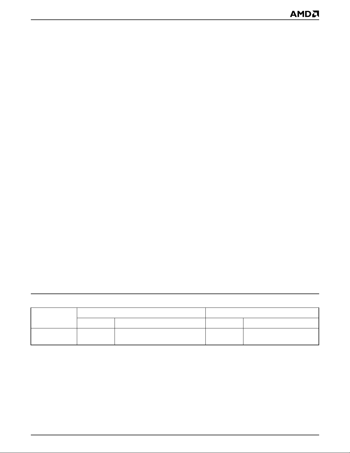
ORDERING INFORMATION
Valid Combination
Order Number Package Marking
DS42514 DS42514
DEVICE BUS OPERATIONS
This section describe s the requirements and use of
the device bus operations, which are initiated through
the internal co mmand reg ister. The comma nd regist er
itself does not occupy any addressable memory location. The register is a latch used to store the
commands, along with the address and data information needed to execu te th e c omm and . The c on ten ts of
the register serve as inputs to the internal state machine. The state machine outputs dictate the function
of the device. Tables 1 through 3 lists the de vice bus
operations, the inputs and control levels they require,
and the resulting output. The following subsections describe each of these operations in further detail.
8 DS42514
Page 9
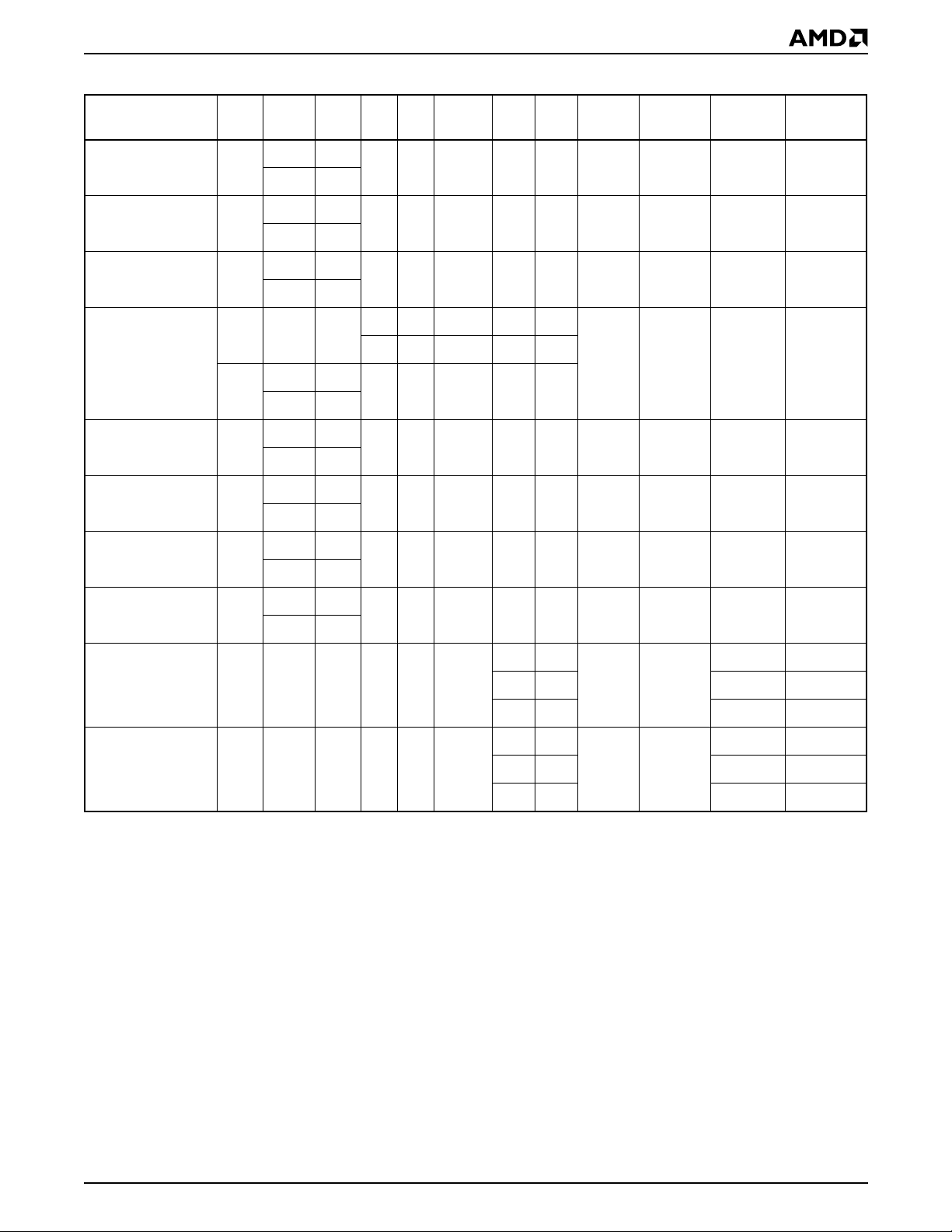
Table 1. Device Bus Operations—Flash Word Mode, CIOf = VIH; SRAM Word Mode, CIOs = VCC
Operation
(Notes 1, 2)
CE#f CE1#s CE2s OE# WE# SA LB#s UB#s RESET#
Read from Flash L
Write to Flash L
Standby
V
0.3 V
Output Disable
Flash Hardware
Reset
Sector Protect
(Note 4)
Sector Unprotect
(Note 4)
HX
XL
HX
XL
HX
±
CC
XL
HLH
HX
L
XL
HX
X
XL
HX
L
XL
HX
L
XL
WP#/ACC
(Note 3)
LH X X X H L/H D
H L X X X H (Note 3) D
±
V
XX X X X
CC
0.3 V
DQ0– DQ7 DQ8–DQ15
OUT
IN
D
OUT
D
IN
HHigh-ZHigh-Z
HH X L X
HH X X L
H L/H High-Z High-Z
HH X X X
X X X X X L L/H High-Z High-Z
HL X X X V
HL X X X V
ID
ID
L/H D
(Note 5) D
IN
IN
X
X
Temporary Sector
Unprotect
X
Read from SRAM H L H L H X
Write to SRAM H L H X L X
HX
XL
XX X X X V
ID
LL
HL High-Z D
HX
LH D
LL
HL High-Z D
HX
(Note 5) D
D
D
IN
OUT
OUT
IN
High-Z
D
OUT
OUT
High-Z
D
IN
IN
LH DINHigh-Z
Legend: L = Logic Low = VIL, H = Logic High = VIH, VID = 8.5–12.5 V, VHH = 9.0 ± 0.5 V, X = Don’t Care, SA = Sector Address,
= Address In, DIN = Data In, D
A
IN
= Data Out
OUT
Notes:
1. Other operations except for those indicated in this column are inhibited.
2. Do not apply CE#f = V
3. If WP#/ACC = V
If WP#/ACC = V
, CE1#s = VIL and CE2s = VIH at the same time.
IL
, the boot sectors will be protected. If WP#/ACC = VIH the boot sectors protection will be removed.
IL
(9V), the program time will be reduced by 40%.
ACC
4. The sector protect and sector unprotect functions may also be implemented via programming equipment. See the “Sector/Sector
Block Protection and Unprotection” section.
5. If WP#/ACC = V
, the two outermost boot sectors remain protected. If WP#/ACC = VIH, the two outermost boot sector protection
IL
depends on whether they were last protected or unprotected using the method described in “Sector/Sector Block Protection and
Unprotection”. If WP#/ACC = V
all sectors will be unprotected.
HH,
DS42514 9
Page 10
Table 2. Device Bus Operations—Flash Word Mode, CIOf = V
Operation
(Notes 1, 2)
CE#f CE1#s CE2s OE# WE# SA
Read from Flash L
Write to Flash L
V
Standby
CC
0.3 V
Output Disable
Flash Hardware
Reset
Sector Protect
(Note 5)
HX
XL
HX
XL
HX
±
XL
HLH
HX
L
XL
HX
X
XL
HX
L
XL
LH X X X H L/H D
H L L X X H (Note 3) D
XX X X X
HH X L X
HH X X L
HH X X X
X X X X X L L/H High-Z High-Z
HL X X X V
LB#s
(Note 3)
UB#s
(Note 3)
; SRAM Byte Mode, CIOs = VSS
IH
CC
±
WP#/ACC
(Note 4)
DQ0–DQ7 DQ8–DQ15
OUT
IN
H High-Z High-Z
RESET#
V
0.3 V
H L/H High-Z High-Z
ID
L/H D
IN
D
OUT
D
IN
X
Sector Unprotect
(Note 5)
Temporary Sector
Unprotect
X
Read from SRAM H L H L H SA X X H X D
Write to SRAM H L H X L SA X X H X D
L
HX
XL
HX
XL
HL X X X V
XX X X X V
ID
ID
(Note 6) D
(Note 6) D
IN
IN
OUT
IN
X
High-Z
High-Z
High-Z
Legend: L = Logic Low = VIL, H = Logic High = VIH, VID = 8.5–12.5 V, VHH = 9.0 ± 0.5 V, X = Don’t Care, SA = Sector Address,
= Address In, DIN = Data In, D
A
IN
= Data Out
OUT
Notes:
1. Other operations except for those indicated in this column are inhibited.
2. Do not apply CE#f = V
, CE1#s = VIL and CE2s = VIH at the same time.
IL
3. Don’t care or open LB#s or UB#s.
4. If WP#/ACC = V
If WP#/ACC = V
, the boot sectors will be protected. If WP#/ACC = VIH the boot sectors protection will be removed.
IL
(9V), the program time will be reduced by 40%.
ACC
5. The sector protect and sector unprotect functions may also be implemented via programming equipment. See the “Sector/Sector
Block Protection and Unprotection” section.
6. If WP#/ACC = V
, the two outermost boot sectors remain protected. If WP#/ACC = VIH, the two outermost boot sector protection
IL
depends on whether they were last protected or unprotected using the method described in “Sector/Sector Block Protection and
Unprotection”. If WP#/AC C = V
all sectors will be unprotected.
HH,
10 DS42514
Page 11
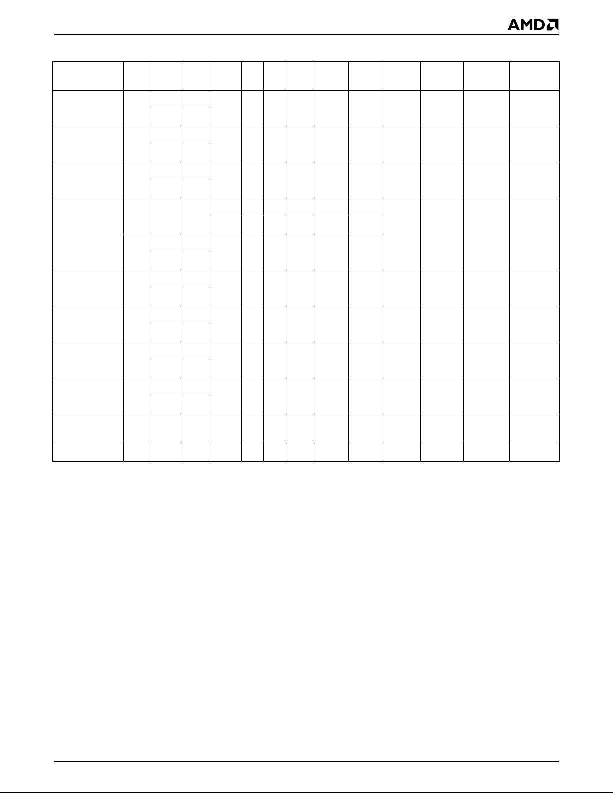
T a ble 3. Device Bus Operations—Flash Byte Mode, CIOf = VIL; SRAM Byte Mode, CIOs = VSS
Operation
(Notes 1, 2 )
CE#f CE1#s CE2s
Read from Flash L
Write to Flash L
V
Standby
CC
0.3 V
Output Disable
Flash Hardware
Reset
Sector Protect
(Note 5)
Sector Unprotect
(Note 5)
DQ15/
HX
XL
HX
XL
HX
±
XL
HLH
HX
L
XL
HX
X
XL
HX
L
XL
HX
L
XL
LB#s
(Note 3)
A–1
OE#
WE# SA
A–1LH X X X H L/H D
A–1HL X X X H
XX X X X
UB#s
(Note 3)
RESET#
±
V
CC
0.3 V
WP#/ACC
(Note 4)
(Note 3)
DQ0–DQ7 DQ8–DQ15
OUT
D
IN
H High-Z High-Z
High-Z
High-Z
XHHX L X
HHXX X L
H L/H High-Z High-Z
A–1HH X X X
X X X X X X L L/H High-Z High-Z
HL X X X V
HL X X X V
ID
ID
L/H D
(Note 6) D
IN
IN
X
X
Temporary
Sector Unprotect
Read from
SRAM
Write to SRAM H L H X X L SA X X H X D
Hx
X
XX X X X V
XL
HLHXLHSAX X H X D
(Note 6) D
ID
IN
OUT
IN
High-Z
High-Z
High-Z
Legend: L = Logic Low = VIL, H = Logic High = VIH, VID = 8.5–12.5 V, VHH = 9.0 ± 0.5 V, X = Don’t Care, SA = Sector Address,
A
= Address In, DIN = Data In, D
IN
= Data Out
OUT
Notes:
1. Other operations except for those indicated in this column are inhibited.
2. Do not apply CE#f = V
, CE1#s = VIL and CE2s = VIH at the same time.
IL
3. Don’t care or open LB#s or UB#s.
4. If WP#/ACC = V
If WP#/ACC = V
, the boot sectors will be protected. If WP#/ACC = VIH the boot sectors protection will be removed.
IL
(9V), the program time will be reduced by 40%.
ACC
5. The sector protect and sector unprotect functions may also be implemented via programming equipment. See the “Sector/Sector
Block Protection and Unprotection” section.
6. If WP#/ACC = V
, the two outermost boot sectors remain protected. If WP#/ACC = VIH, the two outermost boot sector protection
IL
depends on whether they were last protected or unprotected using the method described in “Sector/Sector Block Protection and
Unprotection”. If WP#/AC C = V
all sectors will be unprotected.
HH,
DS42514 11
Page 12

Word/Byte Configuration
The CIOf pin controls whether the device data I/O pins
operate in the byte or word conf iguratio n. If the CIOf
pin is set at lo gic ‘1’, the device is in wor d configuration, DQ0–DQ15 are active and controlled by CE# and
OE#.
If the CIOf pin is set at logic ‘0’, the device is in byte
configuration, and o nly data I/O pi ns DQ0–DQ7 are
active and control led by CE# and OE# . The data I/O
pins DQ8–DQ14 are tri-stated, and the DQ15 pin is
used as an input for the LSB (A-1) address function.
Requirements for Reading Array Data
To read array data from the outputs, the system must
drive the CE#f and OE# pins to V
. CE#f is the power
IL
control and sele cts the de vice. OE# is the outpu t control and gates array data to the output pins. WE#
should remain at V
. The CIOf pin dete rmines
IH
whether the de vice outputs a rray data in word s or
bytes.
The internal state machine is set for reading array data
upon device power-up, or af ter a har dware r eset. This
ensures that no sp urious alteration of th e memory
content occurs during the power transition. No command is necessary in this m ode to obtai n array data .
Standard micropr ocess or read cyc les that asse rt vali d
addresses on the de vice addre ss in puts produ ce vali d
data on the device data outp uts. Each bank remai ns
enabled for read access until the co mmand register
contents are altered.
See “Requirements for Reading Array Data” for more
information. Refer to the AC Flash Read-Only Operations table for timing specifications and to Figure 14 for
the timing diagram. I
in the DC Char acteristics
CC1
table represents the active current specification for
reading array data.
Writing Commands/Command Sequences
To write a command or command sequence (which includes programming data to the device and erasin g
sectors of memory), th e system must driv e WE# an d
CE#f to V
For program operation s, the CIOf pin determines
whether the device accept s program data in by tes or
words. Refer to “Word/Byte Configuration” for more
information.
The device features an Unlock Bypas s mode to facilitate faster programming. Once a bank enters the
Unlock Bypass mode, only two write cycles are required to program a word or byte, instead of four. The
“Word/Byte Configuration” section has details on programming data to the device using both standard and
Unlock Bypass command sequences.
, and OE# to VIH.
IL
An erase operation can erase one sector, multiple sectors, or the entire device. Tables 5–6 indicate the
address space that each sector occupies. The device
address space is divided into two banks: Bank 1 contains the boot/parameter sec tor s, and Ban k 2 co ntai ns
the larger, c ode sectors of uniform size. A “bank address” is the address b its r equ ir ed t o un iqu ely s el ect a
bank. Similarly, a “sector address” is the address bits
required to uniquely select a sector.
in the DC Characteristics table represents the ac-
I
CC2
tive current specification for the write mode. The AC
Characteristics section contains timing specification
tables and timing diagrams for write operations.
Accelerated Program Operation
The device offers accelerated p rogram oper ations
through the ACC function. This is one of two functions
provided by the WP#/ACC pin. This function is primarily intended to allow faster manufacturing throughput
at the factory.
If the system asserts V
on this pin, the devic e auto-
HH
matically enters th e aforemention ed Unlock B ypass
mode, temporarily unprotects any protected sectors,
and uses the h igher vo ltage on the pin to re duce th e
time required for program operations. The system
would use a two-cycle program command sequence
as required by the Unloc k Bypass mo de. Removing
from the WP#/ACC pin returns the device to nor-
V
HH
mal operation. Note that the WP#/ACC pin must not
be at V
for operations other than accelerated pro-
HH
gramming, or device damage may result. In ad dition,
the WP#/ACC pin must not be left floating or unconnected; inconsistent behavior of the device may result.
Autoselect Functions
If the system writes the autoselect command sequence, the device enters the autoselect mode. The
system can then read autosel ect co des from the internal register (which is separate from the memory array)
on DQ7–DQ0. Standar d read cycle timings app ly in
this mode. Refer to the Autoselect Mode and Autoselect Command Sequence sections for more
information.
Simultaneous Read/Write Operations with
Zero Latency
This device is capable of reading data from one bank
of memory while programming or erasing in the other
bank of memory. An erase operation may also be su spended to read from or program to another location
within the same bank (except the sector being
erased). Figu re 21 s hows how read and w rite cycles
may be initiated for simultaneous operation with zero
latency. I
CC6
and I
represent the current specifications for read-while-program and read-while-erase, respectively.
in the DC Characterist ics table
CC7
12 DS42514
Page 13
Standby Mode
When the system is not reading or writing to the device, it can place the device in the standby mode. In
this mode, current consumption is greatly reduced,
and the outputs are placed in the high impedance
state, independent of the OE# input.
The device enters th e CMOS s tandby m ode when th e
CE#f and RESET# pins are both held at V
± 0.3 V.
CC
(Note that this is a more restricted voltage range than
.) If CE#f and RESET# are held at VIH, but not
V
IH
within V
± 0.3 V, the device will be in the standby
CC
mode, but the stan dby cur ren t will b e gr eater. The device requires standard access time (t
) for read
CE
access when the devi ce is in either of these stand by
modes, before it is ready to read data.
If the device is deselecte d during erasur e or programming, the device draws active current until the
operation is completed.
in the DC Characteristics table represents the
I
CC3
standby current specif ic ati on.
Automatic Sleep Mode
The automatic sleep mode minimizes Flash device energy consumption. The device automati cally enables
this mode w hen ad dresses remain s table for t
ACC
+
30 ns. The aut omatic sle ep mode is in dependent o f
the CE#f, WE#, and OE# control signals. Standard address access timi ngs provide new data when
addresses are changed. While in sleep mode, o utput
data is latc hed and always a vailable to the system.
in the DC Characteristics table represents the
I
CC4
automatic sleep mode current specification.
RESET#: Hardware Reset Pin
The RESET# pin provides a hardware method of resetting the device to reading array data. When th e
RESET# pin is driven low for at least a period of t
RP
the device immediately terminates any operation in
progress, tristates all output pins, and ignores all
read/write commands for the duration of the RESET#
pulse. The device al so resets the i nternal state machine to reading arra y data. The o peration that was
interrupted should be reinitiated once the device is
ready to accept another command sequence, to ensure data integrity.
Current is reduced for the duration of the RESET#
pulse. When RESET# is held at V
vice draws CMOS standby current (I
held at V
but not within V
IL
± 0.3 V, the standby cur-
SS
± 0.3 V, the de-
SS
). If RESET# is
CC4
rent will be greater.
The RESET# pin may be tied to the system reset cir-
cuitry. A system reset would thus also reset the Flash
memory, enabling the system to read the boot-up firmware from the Flash memory.
If RESET# is asserted during a program or erase operation, the RY/BY# pin remains a “0” (busy) until the
internal reset operation is complete, which requires a
time of t
(during Embed ded Algorithm s). The
READY
system can thus monitor RY/BY# to determine
whether the reset ope ratio n is co mplete . If RES ET# is
asserted when a program or erase operation is not executing (RY/ BY# pin is “1”), the reset operation is
completed within a time of t
ded Algorithms). The system can read data t
the RESET# pin returns to V
(not during Embed-
READY
.
IH
RH
after
Refer to the AC Characteristics tables for RESET# parameters and to Figure 15 for the timing diagram.
Output Disable Mode
When the OE# input is at VIH, output from the device is
disabled. The output pins are placed in the high
impedance state.
,
Device
Part Number
Am29DL163D 4 Mbit
Megabits Sector Sizes Megabits Sector Sizes
T a ble 4. Device Bank Division
Bank 1 Bank 2
Eight 8 Kbyte/4 Kword,
seven 64 Kbyte/32 Kword
12 Mbit
64 Kbyte/32 Kword
DS42514 13
Twenty-four
Page 14
Table 5. Sector Addresses for Bottom Boot Sector Devices
Sector
Am29DL163DB
SA0 00000000 8/4 000000h–001FFFh 00000h–00FFFh
SA1 00000001 8/4 002000h–003FFFh 01000h–01FFFh
SA2 00000010 8/4 004000h–005FFFh 02000h–02FFFh
SA3 00000011 8/4 006000h–007FFFh 03000h–03FFFh
SA4 00000100 8/4 008000h–009FFFh 04000h–04FFFh
SA5 00000101 8/4 00A000h–00BFFFh 05000h–05FFFh
SA6 00000110 8/4 00C000h–00DFFFh 06000h–06FFFh
Bank 1
Bank 2
Note: The address range is A19:A-1 in byte mode (CIOf=VIL) or A19:A0 in word mode (CIOf=VIH). The bank address bits are A19 and A18 for
Am29DL163DB.
SA7 00000111 8/4 00E000h–00FFFFh 07000h–07FFFh
SA8 00001XXX 64/32 010000h–01FFFFh 08000h–0FFFFh
SA9 00010XXX 64/32 020000h–02FFFFh 10000h–17FFFh
SA10 00011XXX 64/32 030000h–03FFFFh 18000h–1FFFFh
SA11 00100XXX 64/32 040000h–04FFFFh 20000h–27FFFh
SA12 00101XXX 64/32 050000h–05FFFFh 28000h–2FFFFh
SA13 00110XXX 64/32 060000h–06FFFFh 30000h–37FFFh
SA14 00111XXX 64/32 070000h–07FFFFh 38000h–3FFFFh
SA15 01000XXX 64/32 080000h–08FFFFh 40000h–47FFFh
SA16 01001XXX 64/32 090000h–09FFFFh 48000h–4FFFFh
SA17 01010XXX 64/32 0A0000h–0AFFFFh 50000h–57FFFh
SA18 01011XXX 64/32 0B0000h–0BFFFFh 58000h–5FFFFh
SA19 01100XXX 64/32 0C0000h–0CFFFFh 60000h–67FFFh
SA20 01101XXX 64/32 0D0000h–0DFFFFh 68000h–6FFFFh
SA21 01110XXX 64/32 0E0000h–0EFFFFh 70000h–77FFFh
SA22 01111XXX 64/32 0F0000h–0FFFFFh 78000h–7FFFFh
SA23 10000XXX 64/32 100000h–10FFFFh 80000h–87FFFh
SA24 10001XXX 64/32 110000h–11FFFFh 88000h–8FFFFh
SA25 10010XXX 64/32 120000h–12FFFFh 90000h–97FFFh
SA26 10011XXX 64/32 130000h–13FFFFh 98000h–9FFFFh
SA27 10100XXX 64/32 140000h–14FFFFh A0000h–A7FFFh
SA28 10101XXX 64/32 150000h–15FFFFh A8000h–AFFFFh
SA29 10110XXX 64/32 160000h–16FFFFh B0000h–B7FFFh
SA30 10111XXX 64/32 170000h–17FFFFh B8000h–BFFFFh
SA31 11000XXX 64/32 180000h–18FFFFh C0000h–C7FFFh
SA32 11001XXX 64/32 190000h–19FFFFh C8000h–CFFFFh
SA33 11010XXX 64/32 1A0000h–1AFFFFh D0000h–D7FFFh
SA34 11011XXX 64/32 1B0000h–1BFFFFh D8000h–DFFFFh
SA35 11100XXX 64/32 1C0000h–1CFFFFh E0000h–E7FFFh
SA36 11101XXX 64/32 1D0000h–1DFFFFh E8000h–EFFFFh
SA37 11110XXX 64/32 1E0000h–1EFFFFh F0000h–F7FFFh
SA38 11111XXX 64/32 1F0000h–1FFFFFh F8000h–FFFFFh
Sector Address
A19–A12
Sector Size
(Kbytes/Kwords)
(x8)
Address Range
(x16)
Address Range
Table 6. SecSi Sector Addresses for Bottom Boot Devices
Device
Am29DL163DB 00000XXX 64/32 000000h–00FFFFh 00000h–07FFFh
Sector Address
A19–A12
14 DS42514
Sector
Size
(x8)
Address Range
(x16)
Address Range
Page 15
Autoselect Mode
The autoselect mode prov ides manufactur er and device identification, and sector protection verification,
through identifier codes output on DQ7–DQ0. This
mode is primarily intended for programming equipment to automatically match a device to be
programmed wi th its corres ponding pr ogrammin g algorithm. However, the autoselect codes can also be
accessed in-system through the command register.
To access the autoselect codes in-system, the host
system can issue the autoselect command via the
command register, as shown in Table 12. This method
does not require V
. Refer to the Autoselect Com-
ID
mand Sequence section for more information.
Sector/Sector Block Protec ti on and
Unprotection
(Note: For the following discussi on, the term “sector”
applies to both sectors and sector blocks. A sector
block consists of two or more adjacent sectors that are
protected or unprotected at the same time (see Table
7).
Table 7. Bottom Boot Sector/Sector Block
Addresses for Protection/Unpro tect ion
Sector / Sector
Block A19–A12 Sector / Sector Block Size
SA38 11111XXX 64 Kbytes
11110XXX,
SA37
–SA35
–SA31
SA34
SA30
–SA27
SA26
–SA23
SA22
–SA19
–SA15
SA18
SA14
–SA11
–SA8
SA10
SA7 00000111 8 Kbytes
SA6 00000110 8 Kbytes
SA5 00000101 8 Kbytes
SA4 00000100 8 Kbytes
SA3 00000011 8 Kbytes
SA2 00000010 8 Kbytes
SA1 00000001 8 Kbytes
SA0 00000000 8 Kbytes
11101XXX,
11100XXX
110XXXXX 256 (4x64) Kbytes
101XXXXX 256 (4x64) Kbytes
100XXXXX 256 (4x64) Kbytes
011XXXXX 256 (4x64) Kbytes
010XXXXX 256 (4x64) Kbytes
001XXXXX 256 (4x64) Kbytes
00001XXX,
00010XXX,
00011XXX
The hardware sector protection feature disables both
program and erase operations in any sector. The hardware sector unprotection fe ature re-enables both
program and erase operations in previously protected
sectors. Sector protection and unprotection can be implemented as follows.
192 (3x64) Kbytes
192 (3x64) Kbytes
Sector protection/u nprotection requires V
on the RE-
ID
SET# pin only, and can be implemented either
in-system or via programming equipment. Figure 2
shows the algorithms and Figure 26 shows the timing
diagram. This method uses standard m icroprocess or
bus cycle timing. Fo r sector unpr otect, all unprotecte d
sectors must first be protected prior to the first sector
unprotect write cycle. Note that the sector unprotect
algorithm unprotects all sectors in parallel. All previously protected sectors must be individually
re-protected. To change data in protected sectors efficiently, the temporary sector un protect function is
available. See “Temporary Sector/Sector Block
Unprotect”.
The device is shipped with all sectors unprotected.
It is possible to determine whether a secto r is pro-
tected or unprotected. See the Autoselect Mode
section for details.
Write Protect (WP#)
The Write Protect function provides a hardware
method of protecting certai n boot sectors without
using V
. This function is one of two provided by the
ID
WP#/ACC pin.
If the system asserts V
on the WP#/ACC pin, the de-
IL
vice disables program and erase functions in the two
“outermost” 8 Kbyte b oot sectors indep endently of
whether those sectors were protected or unprotected
using the method described in “Sector/Sector Block
Protection and Unprotection”. The two outermost 8
Kbyte boot sectors are the two sectors containing the
lowest addresses in a bottom-boot-configured device,
or the two sectors containin g the highe st addr esses i n
a top-boot-configured device.
If the system asserts V
on the WP#/ACC pin, the de-
IH
vice reverts to whether the two outermost 8 Kbyte boot
sectors were last set to be protected or unp rotected.
That is, sector protecti on or unprotection for these tw o
sectors depends on whether they were last protected
or unprotected using the method desc ribed in “Sec-
tor/Sector Block Protection and Unprotection”.
Note that the WP#/ACC pin must not be left floating or
unconnected; i ncons ist ent be havior of t he devi ce ma y
result.
Temporary Sector/Sector Block Unprotect
(Note: For the foll owing disc ussion, the term “sector”
applies to both sectors and sector blocks. A sector
block consists of two or more adjacent sectors that are
protected or unprotected at the same time (see Table
7).
This feature allows temporary unprotection of previ-
ously protected sectors to change data in-system. The
Sector Unprotect m ode is activa ted by setti ng the RE-
DS42514 15
Page 16
SET# pin to V
(8.5 V – 12.5 V). During this mode,
ID
formerly protected sectors can be programmed or
erased by select ing t he se ctor addr esse s. Onc e V
is
ID
removed from the RESET# pin, all the previously protected sectors are protected again. Figure 1 shows the
algorithm, and Figure 25 shows the timin g diagrams,
for this feature.
START
RESET# = V
(Note 1)
ID
Perform Erase or
Program Operations
RESET# = V
IH
Temporary Sector
Unprotect Completed
(Note 2)
Notes:
1. All protected sectors unprotected (If WP#/ACC = V
outermost boot sectors will remain protected).
2. All previously protected sectors are prote cte d once
again.
,
IL
Figure 1. T emporary Sector Unprotect Operation
16 DS42514
Page 17
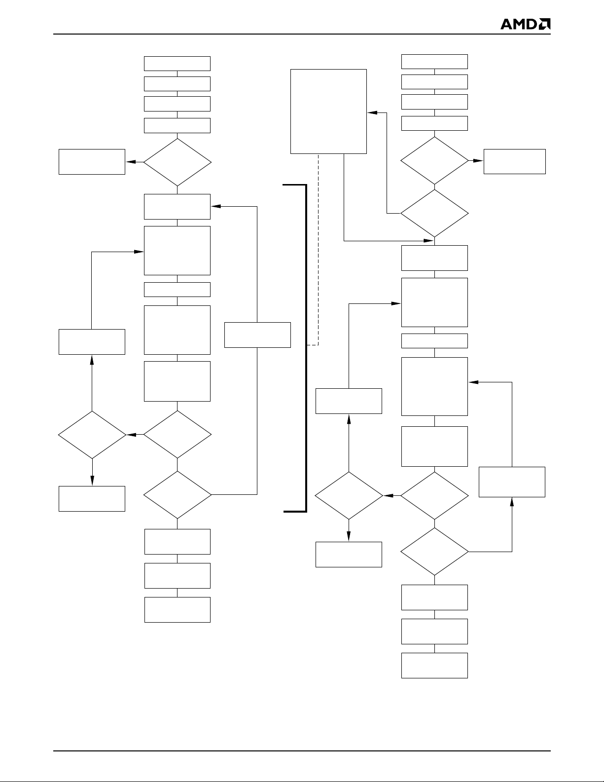
Temporary Sector
Unprotect Mode
Increment
PLSCNT
No
PLSCNT
= 25?
Yes
Device failed
Sector Protect
Algorithm
START
PLSCNT = 1
RESET# = V
Wait 1 µs
No
First Write
Cycle = 60h?
Set up sector
address
Sector Protect:
Write 60h to sector
address with
A6 = 0, A1 = 1,
A0 = 0
Wait 150 µs
Verify Sector
Protect: Write 40h
to sector address
with A6 = 0,
A1 = 1, A0 = 0
Read from
sector address
with A6 = 0,
A1 = 1, A0 = 0
No
Data = 01h?
Protect another
sector?
Remove V
from RESET#
Write reset
command
Sector Protect
complete
Yes
Yes
No
START
Protect all sectors:
The indicated portion
of the sector protect
ID
Reset
PLSCNT = 1
Yes
ID
algorithm must be
performed for all
unprotected sectors
prior to issuing the
first sector
unprotect address
Increment
PLSCNT
No
PLSCNT
= 1000?
Yes
Device failed
Sector Unprotect
PLSCNT = 1
RESET# = V
Wait 1 µs
First Write
Cycle = 60h?
No
All sectors
protected?
Set up first sector
address
Sector Unprotect:
Write 60h to sector
address with
A6 = 1, A1 = 1,
A0 = 0
Wait 15 ms
Verify Sector
Unprotect: Write
40h to sector
address with
A6 = 1, A1 = 1,
A0 = 0
Read from
sector address
with A6 = 1,
A1 = 1, A0 = 0
No
Data = 00h?
Last sector
verified?
Remove V
from RESET#
Yes
Yes
Yes
Yes
ID
No
Temporary Sector
Unprotect Mode
Set up
next sector
address
No
ID
Algorithm
Write reset
command
Note: The term “sector” in the figure applies to both sectors and sector blocks.
Figure 2. In-System Sector/Sector Block Protect and Unprotect Algorithms
DS42514 17
Sector Unprotect
complete
Page 18

SecSi (Secured Silicon) Sector Flash
Memory R egion
The SecSi (Secured Silicon) Sector feature provides a
Flash memory region that enables perm anent part
identification through an Electronic Serial Number
(ESN). The SecSi Sector is 64 Kbytes in length, and
uses a SecSi Sector Indicator Bit to indicate whether
or not the SecSi Sector is locked wh en shipped from
the factory. This bit is permanently set at the factory
and cannot be chan ged, whic h prevents cloning of a
factory locked part. This ensures th e security of the
ESN once the product is shipped to the field.
AMD offers the dev ice with the Sec Si Sector ei ther
factory locked or customer lockable. The factory-locked versi on is al ways p rotec ted wh en shi pped
from the factory, and has the SecSi Sector Indicator
Bit permanently set to a “1.” The customer-lock able
version is shipped with the unprotected, allowing customers to utilize the that sector in any manner they
choose. The custom er-loc kable v ersion has th e Sec Si
Sector Indicator Bit permanently set to a “0.” Thus, the
SecSi Sector Indic ator Bit prev ents cus tomer-loc kable
devices from being used to replace devices that are
factory locked.
The system accesses the SecSi Sector through a
command sequence (s ee “Enter SecSi Sector/Exit
SecSi Sector Comman d Seq uence ”). Afte r the system
has written the Enter SecSi Sector command sequence, it may read the SecSi Sector by using the
addresses normally occupied by the boot sectors. This
mode of operation continues until the system issues
the Exit SecSi Sector command sequence, or until
power is removed from the device. On power-up, or
following a hardware reset, the device reverts to sending commands to the boot sectors.
Factory Locked: SecSi Sector Programmed and
Protected At the Factory
In a factory locked device, the SecSi Sector is protected when the device is shipped from the factory.
The SecSi Sector ca nnot b e mod ified in any w ay. The
device is available preprogrammed with a random, secure ESN only
In devices that have an E SN, a Bottom Boot dev ice
will have the 16 -byte ES N in the lowe st addre ssable
memory area at addresses 00000h–00007h in word
mode (or 000000h–00000Fh in by te mod e) . In the Top
Boot device the starting address of the ESN will be at
the bottom of the lowes t 8 Kbyte boot sector at a ddresses F8000h–F8007h in word mode (or
1F0000h–1F000Fh in byte mode).
Customer Lockable: SecSi Sector NOT
Programmed or Protected At the Factory
If the security feature is not required, the SecSi Sector
can be treated as an additiona l Fl a s h m e mory s p a c e ,
expanding the size of the available Flash array by 64
Kbytes. The SecSi Sector can be read, programmed,
and erased as often as required. Note that the accelerated programming (ACC) and unlock bypass functions
are not available wh en pro gram ming t he SecS i Se cto r.
The SecSi Sector area can be protect ed using o ne of the
following procedures:
■ Write the three-cycle Enter SecSi Sector Region
command sequence, and the n fol low th e in-s ys te m
sector protect algorithm as sho wn in Figure 2, except that RESET# may be at eith er V
or VID. This
IH
allows in-system protection of the without raising
any device pin to a high voltage. Note that this
method is only applicable to the SecSi Sector.
■ Write the three-cycle Enter SecSi Sector Region
command sequence, and then use the alternate
method of sector protection described in the “Sec-
tor/Sector Block Protection and Unprotection”.
Once the SecSi Sec tor i s locke d and v erified, t he system must write the Exit SecSi Sector Region
command sequence to return to reading and writing
the remainder of the array.
The SecSi Sector protection must be used with caution since, once protected, there is no procedure
available for unpro tecting the SecS i Sector area an d
none of the bits in th e SecSi Sect or memory space
can be modified in any way.
Hardware Data Protection
The command sequence r equ irement of unlock cycles
for programming or erasing provides data protection
against inadverten t writes ( refer to Table 12 for command definitions). In addition, the following hardware
data protection measures prevent accidental erasure
or programming , which might ot herwise be cause d by
spurious system level signals during V
and power-down transitions, or from system noise.
Low V
When V
Write Inhibit
CC
is less than V
CC
, the device d oes not ac-
LKO
cept any write cycles. This protects data during V
power-up and power-down. The command register
and all internal program/erase circuits are disabled,
and the device resets to reading array data. Subsequent writes are ignored until V
is greater than V
CC
The system must provide the proper signa ls to the
control pins to prevent unintentional writes when V
is greater than V
LKO
.
power-up
CC
CC
LKO
CC
.
18 DS42514
Page 19

Write Pulse “Glitch” Protection
Noise pulses of less than 5 n s (typi cal) on OE#, CE #f
or WE# do not initiate a write cycle.
Logical Inhibit
Write cycles are inhibited by holding any one of OE# =
V
, CE#f = VIH or WE# = VIH. To in itiate a write cycle ,
IL
CE#f and WE# must be a logical zero while OE# is a
logical one.
Power-Up Write Inhibit
If WE# = CE#f = V
and OE# = VIH during power up,
IL
the device does not accept commands on the rising
edge of WE#. The internal state machine is automatically reset to reading array data on power-up.
COMMON FLASH MEMORY INTERFACE
(CFI)
The Common Flash Interface ( CFI) specific ation outlines device and hos t system software interrogation
handshake, which allows specific vendor-spe cified
software algorithms to be used for entire families of
devices. Software support can then be device-in dependent, JEDEC ID-i ndependent, an d forward- and
backward-compatible for the specified flash device
families. Flash vendors can standardize their existing
interfaces for long-term compatibility.
This device enters the CF I Query mode when the system writes the CFI Quer y command , 98h, to ad dress
55h in word mode (or address AAh in byte mode), any
time the device is ready to read array data. The system can read CFI information at the addresses given
in Tables 8–11. To terminate reading CFI data, the system must write the reset command. The CFI Query
mode is not acces sible wh en the de vice i s executin g
an Embedded Program or embedded erase algorithm.
The system can also write the CFI query command
when the device is in the autoselect mode. The device
enters the CFI query mode, and the system can read
CFI data at the addresses given in Tables 8–11. T he
system must write the reset command to return the device to the autoselect mode.
For further information, please refer to the CFI Specification and CFI Publication 100, available via the
World Wide Web at http://www.amd.com/products/nvd/overview/cfi.html. Alternatively, contact an
AMD representative for copies of these documents.
Addresses
(Word Mode)
10h
11h
12h
13h
14h
15h
16h
17h
18h
19h
1Ah
Addresses
(Byte Mode)
20h
22h
24h
26h
28h
2Ah
2Ch
2Eh
30h
32h
34h
Table 8. CFI Query Identification String
Data Description
0051h
0052h
0059h
0002h
0000h
0040h
0000h
0000h
0000h
0000h
0000h
Query Unique ASCII string “QRY”
Primary OEM Command Set
Address for Primary Extended Table
Alternate OEM Command Set (00h = none exists)
Address for Alternate OEM Extended Table (00h = none exists)
DS42514 19
Page 20

T able 9. System Interface String
Addresses
(Word Mode)
1Bh 36h 0027h
1Ch 38h 0036h
1Dh 3Ah 0000h V
Addresses
(Byte Mode)
Data Description
Min. (write/erase)
V
CC
D7–D4: volt, D3–D0: 100 millivolt
Max. (write/erase)
V
CC
D7–D4: volt, D3–D0: 100 millivolt
Min. voltage (00h = no VPP pin present)
PP
1Eh 3Ch 0000h VPP Max. voltage (00h = no VPP pin present)
1Fh 3Eh 0004h Typical timeout per single byte/word write 2N µs
20h 40h 0000h Typical timeout for Min. size buffer write 2N µs (00h = not supported)
21h 42h 000Ah Typical timeout per individual block erase 2N ms
22h 44h 0000h Typical timeout for full chip erase 2N ms (00h = not supported)
23h 46h 0005h Max. timeout for byte/word write 2N times typical
24h 48h 0000h Max. timeout for buffer write 2N times typical
25h 4Ah 0004h Max. timeout per individual block erase 2N times typical
26h 4Ch 0000h Max. timeout for full chip erase 2N times typical (00h = not supported)
T able 10. Device Geometry Definition
Addresses
(Word Mode)
27h 4Eh 0015h Device Size = 2
28h
29h
2Ah
2Bh
Addresses
(Byte Mode)
50h
52h
54h
56h
Data Description
N
byte
0002h
0000h
0000h
0000h
Flash Device Interface des cri pti on (refe r to CFI publica t io n 100)
Max. number of byte in multi-byte write = 2
(00h = not supported)
2Ch 58h 0002h Number of Erase Block Regions within device
2Dh
2Eh
2Fh
30h
31h
32h
33h
34h
35h
36h
37h
38h
39h
3Ah
3Bh
3Ch
5Ah
5Ch
5Eh
60h
62h
64h
66h
68h
6Ah
6Ch
6Eh
70h
72h
74h
76h
78h
0007h
0000h
0020h
0000h
001Eh
0000h
0000h
0001h
0000h
0000h
0000h
0000h
0000h
0000h
0000h
0000h
Erase Block Region 1 Information
(refer to the CFI specification or CFI publication 100)
Erase Block Region 2 Information
Erase Block Region 3 Information
Erase Block Region 4 Information
N
20 DS42514
Page 21

Table 11. Primary Vendor-Specific Extended Query
Addresses
(Word Mode)
40h
41h
42h
43h 86h 0031h Major version number, ASCII
44h 88h 0031h Minor version number, ASCII
45h 8Ah 0000h
46h 8Ch 0002h
47h 8Eh 0001h
48h 90h 0001h
49h 92h 0004h
4Ah 94h
Addresses
(Byte Mode)
80h
82h
84h
Data Description
0050h
0052h
0049h
00XXh
(See Note)
Query-unique ASCII string “PRI”
Address Sensitive Unlock (Bits 1-0)
0 = Required, 1 = Not Required
Silicon Revision Number (Bits 7-2)
Erase Suspend
0 = Not Supported, 1 = To Read Only, 2 = To Read & Write
Sector Protect
0 = Not Supported, X = Number of sectors in per group
Sector Temporary Unprotect
00 = Not Supported, 01 = Supported
Sector Protect/Unprotect scheme
04 = 29LV800 mode
Simultaneous Operation
00 = Not Supported, X= Number of Sectors in Bank 2 (Uniform Bank)
4Bh 96h 0000h
4Ch 98h 0000h
4Dh 9Ah 0085h
4Eh 9Ch 0095h
4Fh 9Eh 000Xh
Note:
The number of sectors in Bank 2 is device dependent.
Burst Mode Type
00 = Not Supported, 01 = Supported
Page Mode Type
00 = Not Supported, 01 = 4 Word Page, 02 = 8 Word Page
ACC (Acceleration) Supply Minimum
00h = Not Supported, D7-D4: Volt, D3-D0: 100 mV
ACC (Acceleration) Supply Maxim um
00h = Not Supported, D7-D4: Volt, D3-D0: 100 mV
Top/Bottom Boot Sector Flag
02h = Bottom Boot Device, 03h = Top Boot Device
DS42514 21
Page 22

COMMAND DEFINITIO N S
Writing specific address and data commands or sequences into the command register initiates device
operations. Ta ble 12 defines th e valid register command sequences. Writing incorrect address and
data values or writing them in the improper sequence resets the device to reading array data.
All addresses are latched on the falling edge of WE#
or CE#f, whiche ver ha ppens late r. All data is latc hed
on the rising edge of W E# or CE#f, whiche ver happens first. Refer to the AC Characteristics section for
timing diagrams.
Reading Array Data
The device is automati cally set to re ading array dat a
after device power-up. No commands are required to
retrieve data. Each bank is ready to read array data
after completing an Embedded Program or Embedded
Erase algorithm.
After the device accepts an Erase Suspend command,
the corresponding bank enters the erase-suspend-read mode, after which the system can read
data from any non-erase-suspended sector within the
same bank. After completing a programming operation
in the Erase Suspend mode, the system may once
again read array data with the same exception. See
the Erase Suspend/Erase Resume Commands section for more information.
The system must issu e the re set c omm and to r eturn a
bank to the read (or erase-suspend-read) mode if DQ5
goes high during an active program or erase operation, or if the bank is in the autoselect mode. See the
next section, Reset Command, for more information.
See also Requirements for Reading Array Data in the
Device Bus Operations section for more information.
The Flash Read-Only Operations table provides the
read parameters, and Figure 14 shows the timing
diagram.
Reset Command
Writing the reset command resets the banks to the
read or erase-suspend-read mode. Address bits are
don’t cares for this command.
The reset command may be written between the sequence cycles in an erase co mm and s equ enc e befo re
erasing begins. Th is rese ts the b ank to w hich t he system was writing to reading a rray data . Once eras ure
begins, however, the device ignores reset commands
until the operation is complete.
The reset command may be written between the
sequence cycles in a program command sequence
before programming begins. This resets the bank to
which the system was writing to reading array data. If
the program command sequence is written to a bank
that is in the Erase Suspend mode, writing the reset
command returns that ban k to the erase-suspend-read mode. Once programming begins,
however, the device ignores reset comman ds unti l the
operation is complete.
The reset command may be written between the sequence cycles in an autosel ect comm and sequen ce.
Once in the autoselect mode, the reset command
must be written to return to reading array data. If a
bank entered the autoselect mode while in the Erase
Suspend mode, writing the reset command returns
that bank to the erase-suspend-read mode.
If DQ5 goes high during a program or erase operation,
writing the reset command returns the banks to reading array data (or erase-suspend-read mode if that
bank was in Erase Suspend).
Autoselect Command Sequence
The autoselect command sequenc e allows the host
system to access the manufac ture r and de vice codes ,
and determine whether or not a sector is p rotected.
Table 12 shows the address and data requirements.
The autoselect command sequence may be written to
an address within a ba nk that is ei ther in the rea d or
erase-suspend-read mode. The autoselect command
may not be written while the device is actively programming or erasing in the other bank.
The autoselect comm and s equen ce i s init iated by first
writing two unlock cycles. This is followed by a third
write cycle that con tain s t he ba nk add ress an d the autoselect comman d. The bank then enters the
autoselect mode. The system may read at any address within the same bank any number of times
without initiating another autoselect command
sequence:
■ A read cycle at addres s (BA)XX00h (where BA is
the bank address) returns the manufacturer code.
■ A read cy cle at address (BA)X X01h in word mode
(or (BA)XX02h in byte mode) returns the dev ice
code.
■ A read cy cle to an a ddress co ntaining a sector address (SA) within the same bank , and the address
02h on A7–A0 in word mode (or the address 04h on
A6–A-1 in byte mode) returns 01h if the sector is
protected, or 00h if it is unprotected. (Refer to Tables 5–6 for valid sector addre sses ) .
The system must write the reset command to return to
reading array data (or erase-suspend-read mode if the
bank was previously in Erase Suspend).
22 DS42514
Page 23

Enter SecSi Sector/Exit SecSi Sector
Command Sequence
The system can acces s the S ec Si Se ct or re gio n by issuing the thre e-cycle Ente r SecSi S ector co mmand
sequence. The device continues to access the SecSi
Sector region until the sy stem issues the four-cyc le
Exit SecSi Sector command sequence. The Exit SecSi
Sector command sequence returns the device to normal operation. Table 12 shows th e address and data
requirements for bot h com ma nd seq ue nces. Se e also
“SecSi (Secured Silicon) Sector Flash Memory Region” for fu rther information. Note that a har dware
reset (RESET# =V
) will reset the device to reading
IL
array data.
Byte/Word Program Command Sequence
The system may program the device by word or byte,
depending on the state of the CIOf pin. Programming
is a four-bus-cycle operation. The program command
sequence is initiated by writi ng two unlock write cycles, follo wed by th e progr am set-up command . The
program address and data are written next, which in
turn initiate the Embedded Program algorithm. The
system is not required to provide fur ther controls or
timings. The device automatically provides internally
generated program pulses and verifies the programmed cell margin. Table 12 shows the address
and data requirements for the byte program command
sequence.
When the Embedded Program algorithm is complete,
that bank then returns to reading array data and addresses are no longer latched. The system can
determine the status of the prog ram operation by
using DQ7, DQ6, or RY/BY#. Refer to the Write O peration Status se ction for info rmation on the se status
bits.
Any commands written to the device during the Embedded Program Algorithm are i gnored. Note that a
hardware reset immediately terminates the p rogram
operation. The program command sequence should
be reinitiated once th at bank ha s retur ned to readin g
array data, to ensure data integrity.
Programming is allowed in any sequence and across
sector bounda ries. A bit cannot be programmed
from “0” back to a “1.” Attempting to do so may
cause that bank to set DQ5 = 1, or cause the DQ7 and
DQ6 status bits to indicate the operation was success-
ful. However, a succeeding read will show that the
data is still “0.” Only erase operations can convert a
“0” to a “1.”
Unlock Bypass Command Sequence
The unlock bypass feature allows the system to program bytes or words to a bank faster than using the
standard program command sequence. The unlock
bypass command sequence is initiated by first writing
two unlock cycles. Th is is followed by a third write
cycle containing the unlock bypass command, 20h.
That bank then enters the unlock bypass mode. A
two-cycle unlock bypass program command sequence
is all that is requi re d to pr og ram i n t his m ode . T he fir st
cycle in this sequence contains the unlock bypass program command, A0h; the second cycle contains the
program address and data. Additional data is programmed in the same ma nner. This mode dispenses
with the initial two unlock cycles r equired in the standard program command sequence, resulting in faster
total programming time. Table 12 shows the requirements for the command sequence.
During the unlock bypas s mode, on ly the Unlock Bypass Program and Unlock Bypass Reset commands
are valid. To exit the unl ock bypas s mode, th e system
must issue the two-cycle unlock bypass reset command sequence. The fi rst cy cl e m us t c onta in the bank
address and the data 90h. T he second cycle nee d
only contain the data 00h. The bank then returns to
the reading array data.
The device offers accelerated p rogram oper ations
through the WP#/ACC pin. W hen the system asserts
on the WP#/ACC pin, the device automatically en-
V
HH
ters the Unlock Bypass mode. The system may then
write the two-cycle Un lock Bypa ss progr am comman d
sequence. The device uses the higher voltage on the
WP#/ACC pin to accelerate the operation. Note that
the WP#/ACC pin must not be at V
any operation
HH
other than accelerated programmin g, or dev ice damage may result. In addition, the WP#/ACC pin must not
be left floating or unconnected; inconsistent behavior
of the device may result.
Figure 3 illustrates the algorit hm for the prog ra m operation. Refer to the Flash Erase and Program
Operations table in the AC Characteristics section for
parameters, and Figure 18 for timing diagrams.
DS42514 23
Page 24

START
Note: See Table 12 for program command sequence.
Write Program
Command Sequence
mediately terminates the erase operation. If that
occurs, the chip erase command sequence should be
reinitiated once that bank has returned to reading
array data, to ensure data integrity.
Figure 4 illustrates the algorithm for the erase operation. Refer to the Flash Erase and Program
Operations tables in the AC Characteristics section for
parameters, and Figure 20 section for timing
diagrams.
Data Poll
Embedded
Program
algorithm
in progress
Increment Address
No
from System
Verify Data?
Yes
Last Address?
Yes
Programming
Completed
No
Figure 3. Program Operation
Chip Erase Command Sequence
Chip erase is a six bus cycle operation. The chip erase
command sequence is initiated by writing two unlock
cycles, followed by a se t-up c ommand . Two additional
unlock write cycles are then followed by the chip erase
command, which in turn inv ok es th e E mb edde d E ras e
algorithm. The device does not require the system to
preprogram prior to erase. The Embedded Erase algorithm automatically preprograms and verifies the entire
memory for an all zero data patter n prior to e lectrical
erase. The syst em is not r equired to prov ide any co ntrols or timings during these operations. Table 12
shows the address and data r equir ement s for the c hip
erase command sequence.
When the Embedded Erase algor ithm is complete,
that bank returns to reading arr ay data an d address es
are no longer latched. The system can determine the
status of the erase operation by using DQ7, DQ6,
DQ2, or RY/BY#. Refer to the Write Operation Status
section for information on these status bits.
Any commands written during the chip erase operation
are ignored. However, note that a hardware res et im-
Sector Erase Command Sequence
Sector erase is a s ix bus cycle op eration. The sector
erase command sequence is initiated by writing two
unlock cycles, followed by a set-up command. Two additional unlock cycles are wr itten, and are then
followed by the address of the sector to be erased,
and the sector erase command. Table 12 shows the
address and data requirements for the sec tor erase
command sequence.
The device does not require the system to preprogram
prior to erase. The E mbedded E rase algori thm automatically programs and verifies the entire memory for
an all zero da ta patter n prior to electri cal eras e. The
system is not required to provi de any controls or timings during these operations.
After the command sequence is written, a sector erase
time-out of 50 µs occurs. During the time-out period,
additional sector addresses and sector erase commands may be written. Loading the sector erase buffer
may be done in any sequence, and the number of sectors may be from one sector to all sectors. The time
between these additional cycles must be less than
50 µs, other wis e eras ur e m ay beg in. An y sector erase
address and command following the exceeded
time-out may or may not be accepted. It is recommended that proce ssor i nterru pts be disa bled durin g
this time to ensure all commands are accepted. The
interrupts can be re-enabled after the last Sector
Erase command is written. Any command other than
Sector Erase or Erase Suspend during the
time-out period resets that bank to reading array
data. The system must rewrite the command se-
quence and any additional addresses and commands.
The system can monitor DQ3 to determine if the sec-
tor erase timer has timed out (See the section on DQ3:
Sector Erase Timer.). The time-out begins from the rising edge of the final WE# pulse in the command
sequence.
When the Embedded Erase al gor it hm is com pl ete, the
bank returns to readi ng array data an d addr esses a re
no longer latched. Note that while the Embedded
Erase operation is in progress, the system can read
data from the non-erasing bank. T he system can determine the status of the erase operation by reading
DQ7, DQ6, DQ2, or RY/BY# in the erasing bank.
24 DS42514
Page 25

Refer to the Write Oper ation Status section for i nformation on these status bits.
Once the sector erase operation has begun, on ly the
Erase Suspen d command is valid . All other commands are ignored. However, note that a hardware
reset immediately terminates the erase operation. If
that occurs, the sector erase command sequence
should be reinitiated once that bank has returned to
reading array data, to ensure data integrity.
Figure 4 illustrates the algorithm for the erase operation. Refer to the Flash Erase and Program
Operations tables in the AC Characteristics section for
parameters, and Figure 20 section for timing
diagrams.
Erase Suspend/Erase Resume
Commands
The Erase Suspend command, B0h, allows the system to interrupt a sector erase operation and then read
data from, or prog ram data to , a ny s ec tor n ot se lec te d
for erasure. The bank address is required when writing
this command. This command is valid only during the
sector erase operation, including the 50 µs time-out
period during the sector erase command sequence.
The Erase Suspend command is ignored if written during the chip erase oper ation or Embedded P rogram
algorithm.
program operation using the DQ7 or DQ6 status bits,
just as in the standard Byte Program operation.
Refer to the Write Operatio n Status s ection for mor e
information.
In the erase-suspend-rea d mode, the sys tem can als o
issue the autoselec t c om man d s equ ence. Refer to the
Autoselect Mode and Autoselect Command Sequence
sections for details.
To resume the sector erase operation, the system
must write the Erase Resume command. The bank
address of the erase-suspended bank is re quired
when writing this command. Further writes of the Resume comma nd ar e igno red. A nothe r Eras e Su spend
command can be written after the chip has resumed
erasing.
START
Write Erase
Command Sequence
(Notes 1, 2)
When the Erase Suspend command is written during
the sector erase operation, the device requires a maximum of 20 µs to sus pend the erase operation.
However, when the Erase Suspend command is written during the s ector erase time-out, the device
immediately terminates the time-out period and suspends the erase operation.
After the erase operation has been suspended, the
bank enters the erase-susp end-read mode. The system can read data fr om or pr ogram d ata to a ny s ector
not selected for erasure. (The devic e “erase suspends” all sectors s elected for erasure.) Rea ding at
any address within erase-suspended sectors produces status information on DQ7–DQ0. The system
can use DQ7, or DQ6 and DQ 2 tog eth er, to determine
if a sector is actively erasing or is erase-suspended.
Refer to the Write Oper ation Status section for i nformation on these status bits.
After an erase-suspended program operation is complete, the bank r eturns to the era se-suspend-r ead
mode. The system can determine the status of the
Data Poll to Erasing
Bank from System
No
Notes:
1. See Table 12 for erase command sequence.
2. See the section on DQ3 for information on the sector
erase timer.
Data = FFh?
Yes
Erasure Completed
Embedded
Erase
algorithm
in progress
Figure 4. Erase Operation
DS42514 25
Page 26

T able 12. DS42514 Command Definitions
Command
Sequence
(Note 1)
Read (Note 6) 1 RA RD
Reset (Note 7) 1 XXX F0
Manufacturer ID
Device ID
SecSi Sector Factory
Protect (Note 9)
Sector Protect Verify
Autoselect (Note 8)
(Note 10)
Enter SecSi Sector Region
Exit SecSi Sector Region
Program
Unlock Bypass
Unlock Bypass Program (Note 11) 2 XXX A0 PA PD
Unlock Bypass Reset (Note 12) 2 BA 90 XXX 00
Chip Erase
Sector Er ase
Erase Suspend (Note 13) 1 BA B0
Erase Resume (Note 14) 1 BA 30
CFI Query (Note 15)
Legend:
X = Don’t care
RA = Address of th e me mo ry location to be read.
RD = Data read from location RA during read operation.
PA = Address of the memory location to be programmed. Addresses
latch on the fa llin g ed ge of t he WE # o r C E# f pul s e, w hi che ver ha pp ens
later.
Word
4
Byte AAA 555 (BA)AAA
Word
4
Byte AAA 555 (BA)AAA (BA)X02
Word
4
Byte AAA 555 (BA)AAA (BA)X06
Word
4
Byte AAA 555 (BA)AAA (SA)X04
Word
3
Byte AAA 555 AAA
Word
4
Byte AAA 555 AAA
Word
4
Byte AAA 555 AAA
Word
3
Byte AAA 555 AAA
Word
6
Byte AAA 555 AAA AAA 555 AAA
Word
6
Byte AAA 555 AAA AAA 555
Word
1
Byte AA
First Second Third Fourth Fifth Sixth
Cycles
Addr Data Addr Data Addr Data Addr Data Addr Data Addr Data
555
555
555
555
555
555
555
555
555
555
55
AA
AA
AA
AA
AA
AA
AA
AA
AA
AA
98
2AA
2AA
2AA
2AA
2AA
2AA
2AA
2AA
2AA
2AA
Bus Cycles (Notes 2–5)
(BA)555
55
(BA)555
55
(BA)555
55
(BA)555
55
55
55
55
55
55
55
555
555
555
555
555
555
PD = Data to be programmed at location PA. Data latches on the rising
edge of WE# or CE#f pulse, whichever happens first.
SA = Address of the sect or to be veri fi ed (in au t ose lec t mo de ) or
erased. Address bits A19–A12 uniquely select any sector.
BA = Address of th e b an k th at is be ing swi tc h ed to au to s el ect mo de , is
in bypass mode, or is being erased.
90 (BA)X00 01
(BA)X01
90
(BA)X03
90
(SA)X02
90
88
90 XXX 00
A0 PA PD
20
555
80
555
80
81/01
00/01
AA
AA
2AA
2AA
55
55 SA 30
555
10
Notes:
1. See T ables1 through 3 for description of bus operations.
2. All values are in hexadecimal.
3. Except for the read cycle and the fourth cycle of the autoselect
command sequence, all bus cycles are write cycles.
4. Data bits DQ15–DQ8 are don’t care in command sequences,
except for RD and PD.
5. Unless otherwise noted, address bits A19–A11 are don’t cares.
6. No unlock or command cycles required when bank is in read
mode.
7. The Reset command is required to return to reading array data
(or to the erase-suspend-read mode if previously in Erase
Suspend) when a bank is in the autoselect mode, or if DQ5 goes
high (while the bank is providing status information).
8. The fourth cycle of the autoselect command sequence is a read
9. The data is 80h for factory locked and 00h for not factory locked.
10. The data is 00h for an unprotected sector/sector block and 01h
11. The Unlock Bypass command is required prior to the Unlock
12. The Unlock Bypass Reset command is required to return to
13. The system may read and program in non-erasing sectors, or
14. The Erase Resume command is valid only during the Erase
26 DS42514
cycle. The system must provide the bank address to obtain the
manufacturer ID, device ID, or SecSi Sector factory protect
information. Data bits DQ15–DQ8 are don’t care. See the
Autoselect Command Sequence section for more information.
for a protected sector/sector block.
Bypass Program command.
reading array data when the bank is in the unlock bypass mode.
enter the autoselect mode, when in the Erase Suspend mode.
The Erase Suspend command is valid only during a sector erase
operation, and requires the bank address.
Page 27

WRITE OPERATION STATUS
The device provides several bi ts to determ ine the status of a program or erase o peration: DQ2, DQ3, D Q5,
DQ6, and DQ7. Table 13 and the following subs ections describe the function of these bits. DQ7 and DQ6
each offer a method for deter mining wheth er a program or erase operation is comp lete or in progress .
The device also provides a hardware-based output
signal, RY/BY#, to determine whether an Embedded
Program or Erase operation is in progress or has been
completed.
DQ7: Data# Polling
The Data# Polling bit, DQ7, indicates to the host system whether an Embedded Program or Erase
algorithm is in progr ess or completed, or whether a
bank is in Erase Suspend. Data# Polling is valid after
the rising edge of the final WE# pulse in the command
sequence.
During the Embedded Program algorit hm, the device
outputs on DQ7 the complement of the datum programmed to DQ7. This DQ7 s tatus also a pplies to
programming during Erase Suspend. When the Embedded Program algorithm is complete, the device
outputs the datum programmed to DQ7. The system
must provide the progr am add re ss to read v al id sta tus
information on DQ7. If a program address falls within a
protected sector, Data# Polling on DQ7 is active for
approximately 1 µs, then that bank returns to reading
array data.
During the Embedded Erase algorithm, Data# Polling
produces a “0” on DQ7. When the Embedded Erase
algorithm is complete, or if the bank enters the Erase
Suspend mode, Data# Polling produces a “1” on DQ7.
The system must prov ide an a ddr es s w ith in a ny of th e
sectors selected for erasure to read valid status information on DQ7.
After an erase command sequence i s written, if all
sectors selected for e ra sing ar e p ro tected, Data# Polling on DQ7 is active for approximately 100 µs, then
the bank returns to reading a rray data. If no t all selected sectors are protected, the Embedded Erase
algorithm erases the un pr ote cte d sec tor s , a nd ig nor es
the selected sectors that are protected. However, if the
system reads DQ7 at an address within a protected
sector, the status may not be valid.
Just prior to the com pleti on of an E mbed ded P rogram
or Erase operati on, DQ7 may cha nge a syn chro nous ly
with DQ0–DQ6 while Output Enable (OE#) is asserted
low. That is, the device may change from providing
status information to valid data on DQ7. Depending on
when the system samples the DQ7 output, it may read
the status or valid data. Even if the device has com-
pleted the program or erase operation and DQ7 has
valid data, the da ta outputs on DQ0–DQ6 may be still
invalid. Valid data on DQ0–DQ7 will appear on successive read cycles.
Table 13 sho ws the o utput s for Data # Pollin g on DQ7 .
Figure 5 shows the Data# Po lling algorithm . Figure 22
in the AC Characteristics section shows the Data#
Polling timing diagram.
START
Read DQ7–DQ0
Addr = VA
DQ7 = Data?
No
No
Notes:
1. VA = Valid address for programming. During a sector
erase operation, a valid address is any sector address
within the sector being erased. During chip erase, a
valid address is any non-protected sector address.
2. DQ7 should be rechecked even if DQ5 = “1” because
DQ7 may change simultaneously with DQ5.
DQ5 = 1?
Yes
Read DQ7–DQ0
Addr = VA
DQ7 = Data?
No
FAIL
Yes
Yes
PASS
Figure 5. Data# Polling Algorithm
DS42514 27
Page 28
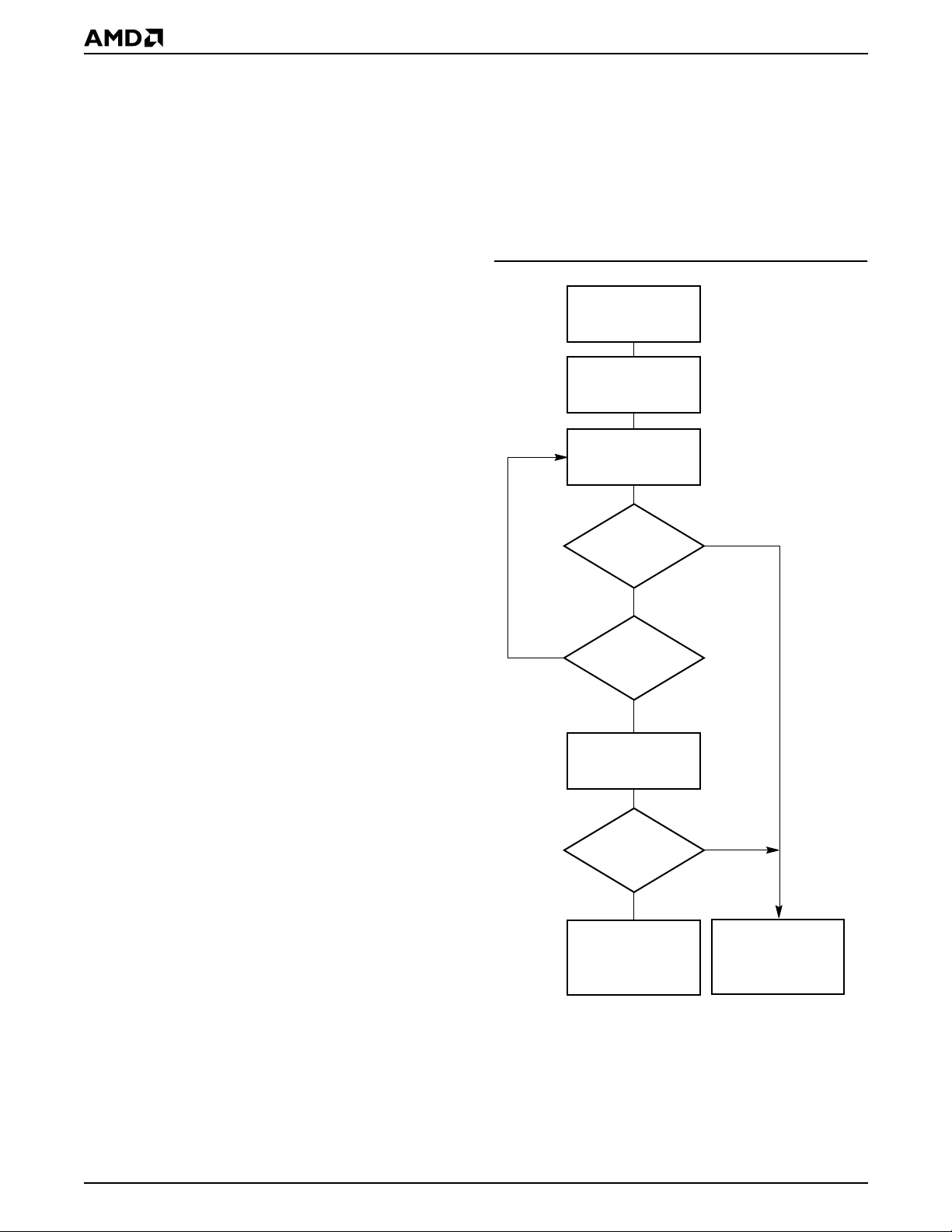
RY/BY#: Ready/Busy#
The RY/BY# is a dedicated, open-drain output pin
which indic ates whe ther an Em bedd ed A lgo rithm is in
progress or complete. The RY/BY# status is valid after
the rising edge of the final WE# pulse in the command
sequence. Since RY/BY# is an open-drain output, several RY/BY# pins can be tied together in parallel with a
pull-up resistor to V
CC
.
If the output is low (Busy), the device is actively erasing or programmin g. (This include s programmi ng in
the Erase Suspend mode.) If the output is high
(Ready), the device is re ading ar ray data, th e stan dby
mode, or one of the banks is in the erase-suspend-read mode.
Table 13 shows the outputs for RY/BY#.
DQ6: T oggle Bit I
Toggle Bit I on DQ6 i ndicates whethe r an Emb edded
Program or Erase algorithm is in progr ess or complete, or whether the device has entered the Erase
Suspend mode. Toggle Bit I may be read at any address, and is valid after the rising edge of the final
WE# pulse in the command sequence ( prior to the
program or erase operation), and during the sector
erase time-out.
DQ6 also toggles during the erase-suspend-pro gram
mode, and stops toggling once the Embedded Program algorithm is complete.
Table 13 shows the outputs for Toggle Bit I on DQ6.
Figure 6 shows the toggle bit algorithm. Figure 23 in
the “AC Charac teristics” section shows the toggle bi t
timing diagrams. Figure 24 shows the differences between DQ2 and DQ6 in graphical for m. See also th e
subsection on DQ2: Toggle Bit II.
START
Read DQ7–DQ0
Read DQ7–DQ0
Toggle Bit
= Toggle?
No
During an Embedded P rogram or Erase alg orithm operation, successive read cycles to any address cause
DQ6 to toggle. The system may use either OE# or
CE#f to control the read cy c les. W hen the operation is
complete, DQ6 stops toggling.
After an erase command sequence i s written, if all
sectors selected for erasing are protected, DQ6 toggles for approxim ately 100 µs , then retur ns to readi ng
array data. If not all selected sectors are protected, the
Embedded Erase algorithm erases the unprotected
sectors, and ignores the selected sectors that are
protected.
The system can use DQ6 and DQ2 together to determine whether a sector is actively erasing or is
erase-suspended. Wh en the device is activel y erasin g
(that is, the Embedded Erase algorithm is in progress),
DQ6 toggles. When the device enters the Erase Suspend mode, DQ6 stops togg li ng. Howe ver, the system
must also use DQ2 to determine which sectors are
erasing or e rase-s usp ended . Al ternat ive ly, the system
can use DQ7 (see the subsection on DQ7: Data#
Polling).
If a program address falls within a protected sector,
DQ6 toggles for approximately 1
µs after the prog ram
command sequence is wri tten, then returns to read ing
array data.
Yes
No
Note: The system shoul d recheck the toggle bit even if DQ5
= “1” because the toggle bit may stop toggling as DQ5
changes to “1.” See the subsections on DQ6 and DQ2 for
more information.
DQ5 = 1?
Yes
Read DQ7–DQ0
Twice
Toggle Bit
= Toggle?
Yes
Program/Erase
Operation Not
Complete, Write
Reset Command
No
Program/Erase
Operation Complete
28 DS42514
Figure 6. Toggle Bit Algorithm
Page 29

DQ2: Toggle Bit II
The “Toggle Bit II” on DQ2, whe n u sed wi th DQ6, indi-
cates whether a particula r sector is actively erasin g
(that is, the Embedded Erase algorithm is in progress),
or whether that sector is erase-suspended. Toggle Bit
II is valid after the rising edge of the final WE# pulse in
the command sequence.
DQ2 toggles when the system reads at addresses
within those sectors that have been selected for erasure. (The system may use either OE# or CE#f to
control the read cycles.) But DQ2 cannot distinguish
whether the s ector i s acti vely era sing or is er ase-s uspended. DQ6, by comparison, indicates whether the
device is actively erasing, or is in Erase Suspend, but
cannot distinguish which sectors are selected for erasure. Thus, both status bits are required for sector and
mode information. Refer to Table 13 to compare outputs for DQ2 and DQ6.
Figure 6 shows the toggle bit algorit hm in flowchart
form, and the se ct ion “DQ 2: Toggle Bit II” explains the
algorithm. See also the DQ6: Toggle Bit I subsection.
Figure 23 shows the toggle bit timing diagram. Figure
24 shows the differences between DQ2 and DQ6 in
graphical form.
Reading Toggle Bits DQ6/DQ2
Refer to Figure 6 for the following discussion. Whenever the system initially begi ns reading toggle bit
status, it must read DQ7–DQ0 at least twic e in a row
to determine whether a toggle bit is tog gl ing. Typically,
the system would note and store the value of the toggle bit after the first read. After the second read, the
system would compare th e new va lue of th e tog gle bit
with the first. If the toggle bit is not toggling, the device
has completed the program or erase operation. The
system can read array data on DQ7–DQ 0 on the following read cycle.
However, if after the initial two read cycles, the system
determines that the toggle bit is still toggling, the system also should note whether the value of DQ5 is high
(see the section on DQ5). If it is, the system should
then determine again whether the toggle bit is toggling, since the toggle bit may ha ve stopped tog gling
just as DQ5 went high . If the toggle bit is no longer
toggling, the device has successfully completed the
program or erase operation. If it is still toggling, the device did not completed the op eration su cces sfull y, and
the system must write th e rese t comma nd to ret urn to
reading array data.
The remaining scenario is that the system initially determines that the toggle bit is toggling and DQ5 has
not gone high. The system may conti nue to monitor
the toggle bit and DQ5 through successive re ad cy-
cles, determ ining the status as de scribed in the
previous paragraph. Alternatively, it may choose to
perform other system tasks. In this case, the system
must start at the beginni ng o f the a lgo rithm when it r eturns to determin e the status of the operat ion (top of
Figure 6).
DQ5: Exceeded Timing Limits
DQ5 indicates whether the program or erase time
has exceeded a specified internal pulse count li mit.
Under these conditions DQ5 produces a “1,” indicating
that the program or erase c ycle was not s uccessfully
completed.
The device may output a “1” on DQ5 if the system tries
to program a “1” to a loc ation that was prev iousl y programmed to “0.” Only an erase opera tion can
change a “0” back to a “1.” Under this condition, the
device halts the operation, and when the timing limit
has been exceeded, DQ5 produces a “1.”
Under both these conditions, the system must write
the reset command to return to reading array data (or
to the erase-suspend-read mode if a bank was previously in the erase-suspend-program mode).
DQ3: Sector Erase Timer
After writing a sect or erase co mmand sequ ence, the
system may read DQ3 to determine whether or not
erasure has begun. (The sector erase timer does not
apply to the chip erase command.) If additional
sectors are selected for erasure, the entire time-out
also applies after each additional sector erase command. When the time-out period is c omplete, DQ3
switches from a “0” to a “1.” If the time between additional sector erase commands from the system can be
assumed to be less than 50 µs, the system need not
monitor DQ3. See also the Sector Erase Command
Sequence section.
After the sector erase comman d is writte n, the syste m
should read the statu s o f D Q7 (D ata # Po llin g) or DQ 6
(Toggle B it I) to ensure that the device has ac cepted
the command sequence, and then read DQ3. If DQ3 is
“1,” the Embedded Erase alg orithm has begun; al l further commands (e xcept E rase Sus pend) ar e ignor ed
until the erase operation is complete. If DQ3 is “0,” the
device will accept additional sector erase commands.
To ensure the command has been accepted, the system software should check the status of DQ3 prior to
and following each subsequent sector erase command. If DQ3 is high on the second status check, the
last command might not have been accepted.
Table 13 show s the sta tus of DQ 3 relativ e to the ot her
status bits.
DS42514 29
Page 30

Table 13. Write Operation Status
Status
Standard
Mode
Erase
Suspend
Mode
Notes:
1. DQ5 switches to ‘1’ when an Embedded Program or Embedded Erase operation has exceeded the maximum timing limits.
Refer to the section on DQ5 for more information.
2. DQ7 and DQ2 require a valid address when reading status information. Refer to the appropriate subsection for further
details.
3. When reading write operation status bi ts, the system must always provide the bank address whe re the Embedde d Algorithm
is in progress. The device outputs array data if the system addresses a non-busy bank.
Embedded Program Algorithm DQ7# Toggle 0 N/A No toggle 0
Embedded E rase Algorithm 0 Toggle 0 1 Toggle 0
Erase
Erase-Suspend-
Read
Erase-Suspend-Program DQ7# Toggle 0 N/A N/A 0
Suspended Sector
Non-Erase
Suspended Sector
DQ7
(Note 2)
1 No toggle 0 N/A Toggle 1
Data Data Data Data Data 1
DQ6
DQ5
(Note 1)
DQ3
DQ2
(Note 2)
RY/BY#
30 DS42514
Page 31

20 ns
20 ns
+0.8 V
–0.5 V
20 ns
–2.0 V
ABSOLUTE MAXIMUM RATINGS
Storage Tempe ra ture
Plastic Packages . . . . . . . . . . . . . . . –55
Ambient Temperature
with Power Applied . . . . . . . . . . . . . . –25
Voltage with Respect to Ground
f/VCCs (Note 1) . . . . . . . . . . . .–0.3 V to +4.0 V
V
CC
OE# and RESET#
(Note 2). . . . . . . . . . . . . . . . . . . .–0.5 V to +12.5 V
WP#/ACC . . . . . . . . . . . . . . . . . .–0.5 V to +10.5 V
All other pins (Note 1). . . . . . –0.5 V to V
Output Short Circuit Current (Note 3) . . . . . . 200 mA
Notes:
1. Minimum DC voltage on input or I/O pins is –0.5 V.
During voltage transitions, input or I/O pins may
overshoot V
Maximum DC voltage on input or I/O pins is V
See Figure 7. During vo lta ge transitions, input or I /O pins
may overshoot to V
Figure 8.
2. Minimum DC input voltage on pins OE#, RESET#, and
WP#/ACC is –0.5 V. During voltage transitions, OE#,
WP#/ACC, and RESET# may oversho ot V
for periods of up to 20 ns. See Figure 7. Maximum DC
input voltage on pin R ESET# is +12.5 V whi ch may
overshoot to +14.0 V for periods up to 20 ns. Maximum
DC input voltage on WP#/ACC is +9.5 V which may
overshoot to +12.0 V for periods up to 20 ns.
3. No more than one output may be shorted to ground at a
time. Duration of the short circuit should not be greater
than one second.
Stresses above those listed under “Absolute Maximum
Ratings” may cause permanent damage to the device. This
is a stress rating only; fu nctional o perati on of the dev ice at
these or any other conditions above those indicated in the
operational sections of this d ata sheet is not implied.
Exposure of the d evice to absolute maximum rating
conditions for extended periods may affect device reliability.
to –2.0 V for periods of up to 20 ns.
SS
+2.0 V for periods up to 2 0 ns. See
CC
°C to +125°C
°C to +85°C
+0.5 V
CC
+0.5 V.
CC
to –2.0 V
SS
OPERATING RANGES
Industrial (I) Devices
Ambient Temper a tur e (T
V
f/VCCs Supply Voltage
CC
f/VCCs for standard voltage range. . 2.7 V to 3.3 V
V
CC
Operating ranges de fine those limits between which the functionality of the device is guaranteed.
) . . . . . . . . .–25°C to +85°C
A
Figure 7. Maximum Negative
Overshoot Waveform
20 ns
V
CC
+2.0 V
V
CC
+0.5 V
2.0 V
20 ns
20 ns
Figure 8. Maximum Positive
Overshoot Waveform
DS42514 31
Page 32

DC CHARACTERISTICS
CMOS Compatible
Parameter
Symbol
I
LI
I
LIT
I
LO
I
LIA
I
f
CC1
f
I
CC2
I
fFlash VCC Standby Current (Note 2)
CC3
fFlash VCC Reset Current (Note 2)
I
CC4
I
f
CC5
f
I
CC6
I
f
CC7
I
f
CC8
Parameter Description Test Conditions Min Typ Max Unit
= VSS to VCC,
V
Input Load Current
RESET# Input Load Current VCC = V
Output Leakage Current
ACC Input Leakage Current
Flash V
Active Read Current
CC
(Notes 1, 2)
Flash V
Active Write Current
CC
(Notes 2, 3)
Flash V
Current Automatic Sleep
CC
Mode (Notes 2, 4)
Flash V
Active
CC
Read-While-Program Curren t (Notes
1, 2)
Flash V
Active Read-While-Erase
CC
Current (Notes 1, 2)
Flash V
Active
CC
Program-While-Erase-Suspended
IN
= VCC
V
CC
V
OUT
V
CC
V
CC
WP#/ACC = V
max
; RESET# = 12.5 V 35 µA
CC max
= VSS to VCC,
= V
CC max
= V
CC max
,
ACC max
CE#f = VIL, OE# = VIH,
Byte Mode
CE#f = V
OE# = VIH,
IL,
Word Mode
CE#f = V
f = V
V
CC
WP#/ACC = V
f = V
V
CC
OE# = VIH, WE# = V
IL,
, CE#f, RESET#,
CC max
CC max
f ± 0.3 V
CC
, RESET# = V
0.3 V, WP#/ACC = V
VCCf = V
= V
V
IL
CE#f = V
CE#f = V
CE#f = V
CC max
± 0.3 V
SS
IL,
, OE# = V
IL
, OE#f = V
IL
, VIH = V
OE# = V
IH
IH
5 MHz 10 16
1 MHz 2 4
5 MHz 10 16
1 MHz 2 4
IL
15 30 mA
0.2 5 µA
±
f ± 0.3 V
CC
CC
SS
± 0.3 V;
0.2 5 µA
0.2 5 µA
Byte 21 45
Word 21 45
Byte 21 45
Word 21 45
IH
17 35 mA
Current (Notes 2, 5)
I
I
CC1
I
CC2
I
CC3
I
CC4
I
CC5
ACC
V
V
ACC Accelerated Program Current,
Word or Byte
sSRAM VCC Active Current
sSRAM VCC Active Current
sSRAM VCC Standby Current
sSRAM VCC Standby Current
CE#f = V
V
CC
CE1#s = V
CE2s = V
s = V
, OE# = V
IL
CC max
,
IL
IH
CE1#s = 0.2 V,
CE2s = V
1) CE1#s = V
2) CE2s = V
CE1#s ≥ V
s – 0.2V
V
CC
s – 0.2V
CC
IH
IL
s – 0.2V , CE2s ≥
CC
,
, CE2s = V
sSRAM VCC Standby Current CE2s ≤ 0.2V 12 µA
Input Low Voltage –0.2 0.8 V
IL
Input High Voltage 2.4 VCC + 0.2 V
IH
ACC pin 5 10 mA
IH
pin 15 30 mA
V
CC
10 MHz 45 mA
10 MHz 45
1 MHz 5
IH
±1.0 µA
±1.0 µA
35 µA
mA
mA
mA
mA
0.3 mA
12 µA
32 DS42514
Page 33

DC CHARACTERISTICS (Continued)
CMOS Compatible
Parameter
Symbol
Parameter Description Test Conditions Min Typ Max Unit
Voltage for WP#/ACC Program
V
Acceleration and Sector
HH
Protection/Unprotection
Voltage for Sector Protection,
V
Autoselect and Temporary Sector
ID
Unprotect
= 4.0 mA, VCCf = VCCs =
I
V
V
OH1
V
OH2
V
LKO
Output Low Voltage
OL
Output Hi gh Voltage
Flash Low VCC Lock-Out Voltage
(Note 5)
OL
V
CC min
= –2.0 mA, VCCf = VCCs =
I
OH
V
CC min
IOH = –100 µA, VCC = V
CC min
Notes:
1. The I
2. Maximum I
current listed is typically less than 2 mA/MHz, with OE# at VIH.
CC
specifications are tested with VCC = VCCmax.
CC
3. ICC active while Embedded Erase or Embedded Program is in progress.
4. Automatic sleep mode enables the low power mode when addresses remain stable for t
200 nA.
5. Not 100% tested.
8.5 9.5 V
8.5 12.5 V
0.45 V
0.85 x
V
CC
VCC–0.4
2.3 2.5 V
+ 30 ns. Typical sleep mode current is
ACC
V
SRAM DC AND OPERATING CHARACTERISTICS
Parameter
Symbol
I
LI
I
LO
I
CC
I
s Average Operating Current
CC1
I
s Average Operating Current
CC2
V
OL
V
OH
I
SB
I
SB1
Parameter Description Test Conditions Min Typ Max Unit
Input Leakage Current VIN = VSS to V
Output Leakage Current
Operating Power Supply Current
CE1#s = V
or WE# = VIL, VIO= VSS to V
V
IH
= 0 mA, CE1#s = VIL, CE2s =
I
IO
WE# = V
CC
, CE2s = VIL or OE# =
IH
, VIN = VIH or V
IH
Cycle time = 1 µs, 100% duty,
= 0 mA, CE1#s ≤ 0.2 V,
I
IO
CE2 ≥ V
V
IN
– 0.2 V, VIN ≤ 0.2 V or
CC
≥ VCC – 0.2 V
Cycle time = Min., I
100% duty, CE1#s = V
V
, VIN = VIL = or V
IH
Output Low Voltage IOL = 2.1 mA 0.4 V
Output Hi gh Voltage IOH = –1.0 mA 2.4 V
Standby Current (TTL)
CE1#s = V
inputs = V
CE2 = VIL, Other
IH,
or V
IH
CE1#s ≥ VCC – 0.2 V, CE2 ≥ VCC –
Standby Current (CMOS)
0.2 V (CE1#s controlled) or CE2 ≤
0.2 V (CE2s controlled), CIOs =
or VCC, Other input = 0 ~ V
V
SS
IL
= 0 mA,
IO
, CE2s =
IL
IH
–1.0 1.0 µA
–1.0 1.0 µA
CC
IL
3mA
5mA
45 mA
0.3 mA
12 µA
CC
DS42514 33
Page 34

DC CHARACTERISTICS
Zero-Power Flash
25
20
15
10
Supply Current in mA
5
0
0 500 1000 1500 2000 2500 3000 3500 4000
Time in ns
Note: Addresses are switching at 1 MHz
Figure 9. I
Current vs. Time (Showing Active and Automatic Sleep Currents)
CC1
12
10
8
6
4
Supply Current in mA
2
3.3 V
2.7 V
0
1 2345
Frequency in MHz
Note: T = 25 °C
Figure 10. Typical I
CC1
34 DS42514
vs. Frequency
Page 35

TEST CONDITIONS
2.7 kΩ
C
L
6.2 kΩ
3.3 V
Device
Under
Test
Note: Diodes are IN3064 or equivalent
Figure 11. Test Setup
Table 14. Test Specifications
Test Condition 85 ns Unit
Output Load 1 TTL gate
KEY TO SWITCHING WAVEFORMS
WAVEFORM INPUTS OUTPUTS
Output Load Capacitance, C
(including jig capacitance)
Input Rise and Fall Times 5 ns
Input Pulse Levels 0.0–3.0 V
Input timing measurement reference
levels
Output timing measurement
reference levels
Steady
Changing from H to L
Changing from L to H
L
30 pF
1.5 V
1.5 V
3.0 V
0.0 V
Don’t Care, Any Change Permitted Changing, State Unknown
Does Not Apply Center Line is High Impedance State (High Z)
KS000010-PAL
1.5 V 1.5 V
Figure 12. Input Waveforms and Measurement Levels
OutputMeasurement LevelInput
DS42514 35
Page 36

AC CHARACTERISTICS
SRAM CE#s Timing
Parameter
Speed
T est Setup
JEDEC Std 85
— t
Description
CE#s Recover Time — Min 0 ns
CCR
E#f
t
CCR
t
CCR
E1#s
t
CCR
t
CCR
E2s
Figure 13. Timing Diagram for Alternating Between SRAM to Flash
Unit
36 DS42514
Page 37
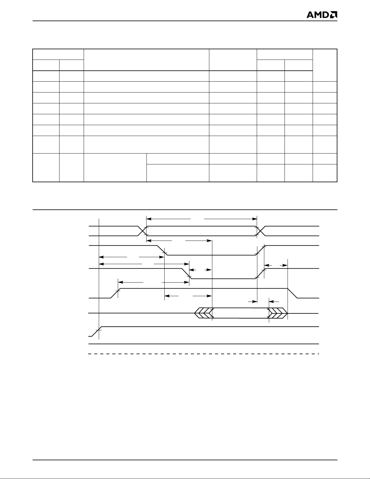
AC CHARACTERISTICS
Flash Read-Only Operations
Parameter
85 ns Speed
Test Setup
JEDEC Std Min Max
t
AVAV
t
AVQV
t
ELQV
t
GLQV
t
EHQZ
t
GHQZ
t
AXQX
Description
t
Read Cycle Time (Note 1) 85 ns
RC
t
Address to Output Delay CE#f, OE# = V
ACC
t
Chip Enable to Output Delay OE# = V
CE
t
Output Enable to Output Delay 35 ns
OE
t
Chip Enable to Output High Z (Note 1) 16 ns
DF
t
Output Enable to Output High Z (Note 1) 16 ns
DF
Output Hold Time From Addresses, CE#f or OE#,
t
OH
Whichever Occurs First
IL
IL
0ns
Read 0 ns
Output Enable Ho ld Time
t
OEH
(Note 1)
Toggle and
Data# Polling
10 ns
Notes:
1. Not 100% tested.
2. See Figure 11 and Table 14 for test specifications.
t
RC
Unit
85 ns
85 ns
Addresses
CE#f
OE#
WE#
Outputs
RESET#
RY/BY#
0 V
Addresses Stable
t
ACC
t
RH
t
RH
t
OEH
t
CE
t
OE
HIGH Z
Figure 14. Read Operation Timings
t
OH
Output Valid
t
DF
HIGH Z
DS42514 37
Page 38

AC CHARACTERISTICS
Hardware Reset (RESET#)
Parameter
JEDEC Std
t
Ready
t
Ready
t
RESET# Pin Low (During Embedded Algorithms)
to Read Mode (See Note)
RESET# Pin Low (NOT During Embedded
Algorithms) to Read Mode (See Note)
RESET# Pulse Width Min 500 ns
t
RP
t
Reset High Time Before Read (See Note) Min 50 ns
RH
RESET# Low to Standby Mode Min 20 µs
RPD
t
RY/BY# Recovery Time Min 0 ns
RB
Note: Not 100% tested.
RY/BY#
CE#f, OE#
RESET#
Description 85 ns Unit
Max 20 µs
Max 500 ns
t
RH
t
RP
t
Ready
Reset Timings NOT during Embedded Algorithms
Reset Timings during Embedded Algorithms
t
Ready
RY/BY#
t
RB
CE#f, OE#
RESET#
t
RP
Figure 15. Reset Timings
38 DS42514
Page 39

AC CHARACTERISTICS
Flash Word/Byte Configuration (CIOf)
Parameter 85 ns Speed
JEDEC Std Description Min Typ Max Unit
t
ELFL/tELFH
t
FLQZ
t
FHQV
CIOf
Switching
from word
to byte
mode
CE#f to CIOf Switching Low or High 5 ns
CIOf Switching Low to Output HIGH Z 30 ns
CIOf Switching High to Output Active 85 ns
CE#f
OE#
CIOf
t
DQ0–DQ14
DQ15/A-1
ELFL
t
ELFH
Data Output
(DQ0–DQ14)
DQ15
Output
t
FLQZ
Data Output
(DQ0–DQ7)
Address
Input
CIOf
CIOf
Switching
from byte
to word
DQ0–DQ14
Data Output
(DQ0–DQ7)
mode
DQ15/A-1
Address
Input
t
FHQV
Figure 16. CIOf Timings for Read Operations
CE#f
The falling edge of the last WE# signal
WE#
CIOf
t
SET
(tAS)
t
HOLD
(tAH)
Note: Refer to the Erase/Program Operations table for tAS and tAH specifications.
Figure 17. CIOf Timings for Write Operations
Data Output
(DQ0–DQ14)
DQ15
Output
DS42514 39
Page 40

AC CHARACTERISTICS
Flash Erase and Program Operations
Parameter 85 ns Speed
JEDEC Std Description Min Typ Max
t
AVAV
t
AVWL
t
WLAX
t
DVWH
t
WHDX
t
t
t
WC
t
ASO
t
AHT
t
t
DH
Write Cycle Time (Note 1) 85 ns
Address Setup Time (WE# to Address) 0 ns
AS
Address Setup Time to OE# or CE#f low during toggle bit
polling
Address Hold Time (WE# to Address) 45 ns
AH
Address Hold Time From CE#f or OE# high during toggle bit
polling
Data Setup Time 35 ns
DS
15 ns
0ns
Data Hold Time 0 ns
Read 0 ns
t
GHEL
t
GHWL
t
WLEL
t
ELWL
t
EHWH
t
WHEH
t
WLWH
t
ELEH
t
WHDL
t
OEH
t
OEPH
t
GHEL
t
GHWL
t
WS
t
t
WH
t
CH
t
WP
t
t
WPH
t
SR/W
OE# Hold Time
Toggle and Data# Polling 10 ns
Output Enable High during toggle bit polling 20 20 20 ns
Read Recovery Time Before Write (OE# High to CE#f Low) 0 ns
Read Recovery Time Before Write (OE# High to WE# Low) 0 ns
WE# Setup Time (CE#f to WE#) 0 ns
CE#f Setup Time (WE# to CE#f) 0 ns
CS
WE# Hold Time (CE#f to WE#) 0 ns
CE#f Hold Time (CE#f to WE#) 0 ns
Write Pulse Width 35 ns
CE#f Pulse Width 35 ns
CP
Write Pulse Width High 30 ns
Latency Between Read and Write Operations 0 ns
Byte 5
t
WHWH1
t
WHWH1
Programming Operation (Note 2)
Word 7
Unit
µs
t
WHWH1
t
WHWH2
t
WHWH1
t
WHWH2
t
VCS
t
t
BUSY
Accelerated Programming Operation,
Word or Byte (Note 2)
Sector Erase Operation (Note 2) 0.7 sec
VCCf Setup Time (Note 1) 50 µs
Write Recovery Time from RY/BY# 0 ns
RB
Program/Erase Valid to RY/BY# Delay 90 ns
Notes:
1. Not 100% tested.
2. See the “Flash Erase And Programming Performance” section for more information.
40 DS42514
4µs
Page 41

AC CHARACTERISTICS
Addresses
CE#f
OE#
WE#
Data
RY/BY#
V
CC
Program Command Sequence (last two cycles)
DH
t
AS
PA PA
t
AH
t
CH
t
WPH
PD
t
BUSY
t
WC
555h
t
GHWL
t
CS
t
WP
t
DS
t
A0h
Read Status Data (last two cycles)
PA
t
WHWH1
Status
D
OUT
t
RB
f
t
VCS
otes:
. PA = program address, PD = program data, D
. Illustration shows device in word mod e.
Figure 18. Program Operation Timings
V
HH
V
or V
IL
WP#/ACC
IH V
t
VHH
Figure 19. Accelerated Program Timing Diagram
is the true data at the program address.
OUT
t
VHH
IL
or V
IH
DS42514 41
Page 42

AC CHARACTERISTICS
Erase Command Sequence (last two cycles) Read Status Data
t
AS
555h for chip erase
VA
t
AH
VA
Addresses
t
WC
2AAh SA
CE#f
t
GHWL
t
t
CH
WP
OE#
WE#
Data
t
DH
WPH
30h
10 for Chip Erase
t
BUSY
t
CS
t
DS
t
55h
t
WHWH2
In
Progress
Complete
t
RB
RY/BY#
t
VCS
f
V
CC
otes:
. SA = sector address (for Sector Erase), VA = Valid Address for reading status data (see “Write Operation Status”).
. These waveforms are for the word mode.
Figure 20. Chip/Sector Erase Operation Timings
42 DS42514
Page 43

AC CHARACTERISTICS
Addresses
CE#f
OE#
WE#
Data
t
WPH
t
WC
Valid PA
t
AH
t
WP
t
DS
Valid
In
t
DH
t
OEH
t
RC
Valid RA
t
ACC
t
CE
t
SR/W
t
OE
t
OH
Valid
Out
Read Cycle
t
DF
t
GHWL
Figure 21. Back-to-back Read/Write Cycle Timings
t
WC
Valid PA
Valid
In
CE#f Controlled Write CyclesWE# Controlled Write Cycle
t
CPH
t
WC
Valid PA
Valid
In
t
CP
t
RC
Addresses
t
ACC
VA
t
CE
VA VA
CE#f
t
CH
t
OE
OE#
t
OEH
t
DF
WE#
t
DQ7
DQ0–DQ6
t
BUSY
OH
Complement
Status Data
Complement
Status Data
True
True
Valid Data
Valid Data
High Z
High Z
RY/BY#
Note: VA = Valid address. Illustration shows first status cycle after command sequence, last status read cycle, and array data
read cycle.
Figure 22. Data# Polling Timings (During Embedded Algorithms)
DS42514 43
Page 44

AC CHARACTERISTICS
t
AHT
Addresses
t
ASO
CE#f
t
OEH
WE#
OE#
t
DH
DQ6/DQ2 Valid Data
RY/BY#
Valid Data
(first read) (second read) (stops toggling)
Valid
Status
t
OEPH
t
OE
Valid
Status
t
CEPH
t
t
AHT
AS
Valid
Status
Note: VA = V alid address ; not required for DQ6. Illust ration shows first two statu s cycle after command se quence, last status re ad
cycle, and array data read cycle
Figure 23. Toggle Bit Timings (During Embedded Algorithms)
Enter
Embedded
Erasing
WE#
Erase
Erase
Suspend
Erase Suspend
Suspend Program
Read
Enter Erase
Erase
Suspend
Program
Erase Suspend
Read
Erase
Resume
Erase
Erase
Complete
DQ6
DQ2
Note: DQ2 toggles only when read at an address within an erase-suspended sector. The system may use OE# or CE#f to
toggle DQ2 and DQ6.
Figure 24. DQ2 vs. DQ6
44 DS42514
Page 45

AC CHARACTERISTICS
Temporary Sector/Sector Block Unprotect
Parameter
JEDEC Std Description
t
VID Rise and Fall Time (See Note) Min 500 ns
VIDR
t
VHH Rise and Fall Time (See Note) Min 250 ns
VHH
RESET# Setup Time for Temporary
t
RSP
Sector/Sector Block Unprotect
RESET# Hold Time from RY/BY# High for
t
RRB
Temporary Sector/Sector Block Unprotect
Note: Not 100% tested.
V
ID
RESET#
VSS, VIL,
or V
IH
t
CE#f
VIDR
Min 4 µs
Min 4 µs
Program or Erase Command Sequence
85 ns Speed Unit
V
ID
VSS, VIL,
or V
IH
t
VIDR
WE#
RY/BY#
t
RSP
t
RRB
Figure 25. Temporary Sector/Sector Block Unprotect Timing Diagram
DS42514 45
Page 46

AC CHARACTERISTICS
V
ID
V
RESET#
IH
SA, A6,
A1, A0
Valid* Valid* Valid*
Sector/Sector Block Protect or Unprotect Verify
Data
60h 60h 40h
Sector/Sector Block Protect: 150 µs,
Sector/Sector Block Unprotect: 15 ms
1 µs
CE#f
WE#
OE#
* For sector protect, A6 = 0, A1 = 1, A0 = 0. For sector unprotect, A6 = 1, A1 = 1, A0 = 0.
Figure 26. Sector/Sector Block Protect and Unprotect Timing Diagram
Status
46 DS42514
Page 47

AC CHARACTERISTICS
Alternate CE#f Controlled Erase and Program Operations
Parameter 85 ns Speed
JEDEC Std Description Min Typ Max Unit
t
AVAV
t
AVWL
t
ELAX
t
DVEH
t
EHDX
t
GHEL
t
WLEL
t
EHWH
t
ELEH
t
EHEL
t
WHWH1
t
WHWH1
t
WC
t
AS
t
ASO
t
AH
t
AHT
t
DS
t
DH
t
GHEL
t
WS
t
WH
t
CP
t
CPH
t
WHWH1
t
WHWH1
Write Cycle Time (Note 1) 85 ns
Address Setup Time (WE# to Address) 0 ns
Address Setup Time to CE#f Low During Toggle
Bit Polling
15 ns
Address Hold Time 45 ns
Address Hold time from CE# f or O E# High Duri ng
Toggle Bit Polling
0ns
Data Setup Time 35 ns
Data Hold Time 0 ns
Read Recovery Time Before Write
(OE# High to WE# Low)
0ns
WE# Setup Time 0 ns
WE# Hold Time 0 ns
CE#f Pulse Width 35 ns
CE#f Pulse Width High 35 ns
Programming Operation
(Note 2)
Accelerated Programming Operation,
Word or Byte (Note 2)
Byte 5
µs
Word 7
4µs
t
WHWH2
t
WHWH2
Sector Erase Operation (Note 2) 0.7 sec
Notes:
1. Not 100% tested.
2. See the “Flash Erase And Programming Performance” section for more information.
DS42514 47
Page 48

AC CHARACTERISTICS
Addresses
WE#
OE#
CE#f
Data
RESET#
555 for program
2AA for erase
t
WC
t
WH
t
WS
t
RH
PA for program
SA for sector erase
555 for chip erase
t
AS
t
GHEL
t
CP
t
CPH
t
DS
t
DH
A0 for program
55 for erase
t
AH
t
BUSY
PD for program
30 for sector erase
10 for chip erase
Data# Polling
t
WHWH1 or 2
PA
DQ7# D
OUT
RY/BY#
Notes:
1. Figure indicates last two bus cycles of a program or erase operation.
2. PA = program address, SA = sector address, PD = program data.
3. DQ7# is the complement of the data written to the device. D
is the data written to the device.
OUT
4. Waveforms are for the word mode.
Figure 27. Flash Alternate CE#f Controlled Write (Erase/Program) Operation Timings
48 DS42514
Page 49

AC CHARACTERISTICS
SRAM Read Cycle
Parameter
Symbol
t
RC
t
AA
t
, t
CO1
CO2
t
OE
t
BA
t
, t
LZ1
LZ2
t
BLZ
t
OLZ
t
, t
HZ1
HZ2
t
BHZ
t
OHZ
t
OH
Description Min Max Unit
Read Cycle T ime 85 ns
Address Access Time 85 ns
Chip Enable to Output 85 ns
Output Enable Access Time 45 ns
LB#s, UB#s to Valid Output 85 ns
Chip Enable (CE1#s Low and CE2s High) to Low-Z Output 10 ns
UB#, LB# Enable to Low-Z Output 10 ns
Output Enable to Low-Z Output 5 ns
Chip disable to High-Z Outpu t 0 25 ns
UB#s, LB#s Disable to High-Z Output 0 25 ns
Output Disable to High-Z Output 0 25 ns
Output Data Hold from Address Change 15 ns
ddress
ata Out Previous Data Valid
t
OH
t
RC
t
AA
Data Valid
Note: CE1#s = OE# = VIL, CE2s = WE# = VIH, UB#s and/or LB#s = V
Figure 28. SRAM Read Cycle—Ad dre ss Contr olled
IL
DS42514 49
Page 50

AC CHARACTERISTICS
Address
CS#1
t
AA
t
CO1
t
RC
t
OH
CS2
UB#, LB#
OE#
Data Out
High-Z
Figure 29. SRAM Read Cycle
Notes:
1. WE# = V
and t
2. t
HZ
voltage levels.
3. At any given temperature and voltage condition, t
interconnection.
, if CIOs is low, ignore UB#s/LB#s timing.
IH
are defined as the time at which the outputs achieve the open circuit conditions and are not referenced to output
OHZ
t
CO2
t
BA
t
OE
t
OLZ
t
BLZ
t
LZ
(Max.) is less than tLZ (Min.) both for a given device and from device to device
HZ
Data Valid
t
t
OHZ
BHZ
t
HZ
50 DS42514
Page 51

AC CHARACTERISTICS
SRAM Write Cycle
Parameter
Symbol
t
WC
t
Cw
t
AS
t
AW
t
BW
t
WP
t
WR
t
WHZ
t
DW
t
DH
t
OW
Address
CS1#s
CS2s
UB#s, LB#s
Description Min Max Unit
Write Cycle Time 85 ns
Chip Enable to End of Write 70 ns
Address Setup Time 0 ns
Address Valid to End of Write 70 ns
UB#s, LB#s to End of Write 70 ns
Write Pulse Time 60 ns
Write Recovery Time 0 ns
Write to Output High-Z 0 25 ns
Data to Write Time Overlap 35 ns
Data Hold from Write Time 0 ns
End Write to Output Low-Z 5 ns
t
WC
t
CW
(See Note 1)
t
AW
t
CW
(See Note 2)
t
WR
(See Note 1)
t
BW
t
WP
WE#
Data In
Data Out
t
AS
(See Note 3)
High-Z
Data Undefined
(See Note 4)
t
BW
t
DW
Data Valid
t
DH
High-Z
t
OW
Notes:
1. WE# controlled, if CIOs is low, ignore UB#s and LB#s timing.
is measured from CE1#s going low to the end of write.
2. t
CW
3. t
is measured from the end of write to the address change. tWR applied in case a write ends as CE1#s or WE# going high.
WR
4. tAS is measured from the address valid to the beginning of write.
5. A write occurs during the overlap (tWP) of low CE#1 and low WE#. A write begins when CE1#s goes low and WE# goes low when
asserting UB#s or LB#s for a single byte operation or simultaneously asserting UB#s and LB#s for a double byte operation. A
write ends at the earliest transition when CE1#s goes high and WE# goes high. The t
is measured from the beginning of write
WP
to the end of write.
Figure 30. SRAM Write Cycle—WE# Control
DS42514 51
Page 52

AC CHARACTERISTICS
Address
CE1#s
CE2s
UB#s, LB#s
WE#
Data In
t
(See Note 2 )
AS
t
WC
t
CW
(See Note 3)
t
AW
t
BW
(See Note 5)
t
WP
t
DW
Data Valid
t
(See Note 4)
WR
t
DH
Data Out
High-Z High-Z
Notes:
1. CE1#s controlled, if CIOs is low, ignore UB#s and LB#s timing.
is measured from CE1#s going low to the end of write.
2. t
CW
3. tWR is measured from the end of write to the address change. tWR applied in case a write ends as CE1#s or WE# going high.
4. t
is measured from the address valid to the beginning of write.
AS
5. A write occurs during the overlap (tWP) of low CE#1 and low WE#. A write begins when CE1#s goes low and WE# goes low when
asserting UB#s or LB#s for a single byte operation or simultaneously asserting UB#s and LB#s for a double byte operation. A
write ends at the earliest transition when CE1#s goes high and WE# goes high. The tWP is measured from the beginning of write
to the end of write.
Figure 31. SRAM Write Cycle—CE1#s Control
52 DS42514
Page 53

AC CHARACTERISTICS
Address
CE1#s
CE2s
UB#s, LB#s
WE#
Data In
t
AS
(See Note 4)
t
WC
t
CW
(See Note 2)
t
AW
t
(See Note 2)
CW
t
BW
(See Note 5)
t
WP
t
DW
Data Valid
t
(See Note 3)
WR
t
DH
Data Out
High-Z
High-Z
Notes:
1. UB#s and LB#s controlled, CIOs must be high.
is measured from CE1#s going low to the end of write.
2. t
CW
3. tWR is measured from the end of write to the address change. tWR applied in case a write ends as CE1#s or WE# going high.
4. t
is measured from the address valid to the beginning of write.
AS
5. A write occurs during the overlap (tWP) of low CE#1 and low WE#. A write begins when CE1#s goes low and WE# goes low when
asserting UB#s or LB#s for a single byte operation or simultaneously asserting UB#s and LB#s for a double byte operation. A
write ends at the earliest transition when CE1#s goes high and WE# goes high. The tWP is measured from the beginning of write
to the end of write.
Figure 32. SRAM Write Cycle—UB#s and LB#s Control
DS42514 53
Page 54

FLASH ERASE AND PROGRAMMING PERFORMANCE
Parameter Typ (Note 1) Max (Note 2) Unit Comments
Sector Erase Time 0.7 15 sec
Chip Erase Time 27 sec
Excludes 00h programming
prior to erasure (Note 4)
Byte Program Time 5 150 µs
Word Program Time 7 210 µs
Accelerated Byte/Word Program Time 4 120 µs
Chip Program Time
(Note 3)
Byte Mode 9 27
sec
Word Mode 6 18
Excludes system lev el
overhead (Note 5)
Notes:
1. Typical program and erase times assume the following conditions: 25°C, 3.0 V V
, 1,000,000 cycles. Additi ona lly,
CC
programming typicals assume checkerboard pattern.
2. Under worst case conditions of 90°C, V
= 2.7 V, 1,000,000 cycles.
CC
3. The typical chip programming time is considerably less than the maximum chip programming time listed, since most bytes
program faster than the maximum program times listed.
4. In the pre-programming step of the Embedded Erase algorithm, all bytes are programmed to 00h before erasure.
5. System-level overhead is the time required to execute the two- or four-bus-cycle sequence for the program command. See Table
12 for further information on command definitions.
6. The device has a minimum erase and program cycle endurance of 1,000,000 cycles.
FLASH LATCHUP CHARACTERISTICS
Description Min Max
Input voltage with respect to V
(including OE# and RESET#)
Input voltage with respect to V
on all pins except I/O pins
SS
on all I/O pins –1.0 V VCC + 1.0 V
SS
–1.0 V 12.5 V
VCC Current –100 mA +100 mA
Note: Includes all pins except VCC. Test conditions: VCC = 3.0 V, one pin at a time.
PACKAGE PIN CAPACITANCE
Parameter
Symbol Description
C
IN
C
OUT
C
IN2
C
IN3
Input Capacitance VIN = 0 11 14 pF
Output Capacitance V
Control Pin Capacitance VIN = 0 14 16 pF
WP#/ACC Pin Capacitance VIN = 0 17 20 pF
Note: 7.Test conditions TA = 25°C, f = 1.0 MHz.
T est Setup Typ Max Unit
= 0 12 16 pF
OUT
FLASH DATA RETENTION
Parameter Description Test Conditions Min Unit
Minimum Pattern Data Retention Time
150°C10Years
125°C20Years
54 DS42514
Page 55

SRAM DATA RETENTION CHARACTERISTICS
Parameter
Symbol
V
DR
V
DH
t
SDR
t
RDR
Parameter Description
Test Setup
Min Typ Max Unit
VCC for Data Retention CS1#s ≥ VCC – 0.2 V (See Note) 1.5 3.3 V
= 1.5 V, CE1#s ≥ VCC – 0.2 V
V
Data Retention Current
Data Retention Set-Up Time
CC
(See Note)
0.5 5 µA
0ns
See data retention waveforms
Recovery Time t
RC
Note: CE1#s ≥ VCC – 0.2 V, CE 2s ≥ VCC – 0.2 V (CE1#s controlled) or CE2s ≤ 0.2 V (CE2s controlled), CIOs = VSS or VCC.
t
V
CC
SDR
Data Retention Mode
t
RDR
2.7V
2.2V
V
DR
CE1#s
≥
CE1#s
GND
VCC - 0.2 V
Figure 33. CE1#s Controlled Data Retention Mode
ns
V
CC
2.7 V
CE2s
V
DR
0.4 V
GND
Data Retention Mode
t
SDR
CE2s £ 0.2 V
Figure 34. CE2s Controlled Data Retention Mode
t
RDR
DS42514 55
Page 56

PHYSICAL DIMENSIONS
FLA069—69-Ball Fine-Pitch Grid Array 8 x 11 mm
1.40 (max)
0.15
C
(2x)
8.00 BSC
0.97
1.07
11.00 BSC
B
Pin A1
Corner Index Mark
DATUM A
A
DATUM B
0.15
(2x)
C
0.20
C
7.20 BSC
0.20 (min)
0.40
0.80
7.20 BSC
0.40
0.25
0.35
0.80
(69x)
0.15
0.08
M
M
ABCDEFGHJK
CA
C
C
10
9
8
7
6
5
4
3
2
1
B
0.08
C
56 DS42514
Page 57

REVISION SUMMARY
Revision A (July 10, 200 0)
Initial release as Preliminary Draft.
Revision B (December 13, 2000)
Global
Deleted Preliminary status from document. Added
table of contents.
Command Definitions
Ta ble 12, Comm and Defi nitions: The SecSi Sector Indicator Bit values have changed from 80h and 00h to
81h and 01h, respectively.
AC Characteristics—Alternate CE#f Controlled
Erase and Program Operations
t
byte value of 9 µs to 5 µs and the typical word value of
11 µs to 7 µs.
t
rected typical value of 7 µs to 4 µs.
Programming Operation: Corrected typical
WHWH1
Accelerated Programming Operation: Cor-
WHWH1
Revision B+1 (March 7, 2001)
Sector/Sector Block Protec ti on/ Unpr ote ctio n
Added to se cond para grap h: “Note that the sector unprotect algorithm unprotects all sectors in parallel. All
previously pro tected sector s must be individu ally
re-protected. To change data in protected sectors efficiently, the temporary sector unprotect function is
available. See “Temporary Sector/Sector Block
Unprotect”.”
Customer Lockable: SecSi Sector NOT
Programmed or Protected At the Factory
Added to end of first parag raph: “Note that the accelerated programming (ACC) and unlock bypass functions
are not available wh en pro gram ming t he SecS i Se cto r.”
Common Flash Memory Interface (CFI)
Added to second paragraph: “The CFI Query mode is
not accessible when the device is executing an Embedded Program or embedded erase algorithm.”
Revision B+2 (March 15, 2001)
Added “Am29DL163D Bottom Boot” to the product description on the top portion of the first page.
Trademarks
Copyright © 2001 Advanced Micro Devices, Inc. All rights reserved.
AMD, the AMD logo, and combinations thereof are registered trademarks of Advanced Micro Devices, Inc.
ExpressFlash is a trademark of Advanced Micro Devices, Inc.
Product names used in this publication are for identification purposes only and may be trademarks of their respective companies.
DS42514 57
 Loading...