

Page 1

Am186ER and Am188ER
Microcontrollers
User’s Manual
FT
RA
D
Page 2

© 1997 Advanced Micro Devices, Inc. All rights reserved.
Advanced Micro Devices, Inc. (“AM D”) reserves the right to make changes in
its products without notice in order to improve design or performance characteristics.
The information in this publication is believed to be accurate at the time of publication, but AMD makes no representations or warranties with
respect to the accuracy or completeness of the contents of this publication or the information contained herein, and reserves the right to make
changes at any time, without notice. AMD disclaims responsibility for any consequences resulting from the use of the information included in this
publication.
This publication neither states nor implies any representations or warranties of any kind, including but not limited to, any implied w arranty of
merchantability or fitness for a particular purpose. AMD products are not authorized for use as critical components in life support devices or
systems without AMD’s written approval. AMD assumes no liability whatsoever for claims assoc iated with the sale or use (including the use of
engineering samples) of AMD products except as provided in AMD’s Terms and Conditions of Sale for such products.
Trademarks
AMD, the AMD logo, and combinations thereof are trademarks of Advanced Micro Devices, Inc.
Am386 and Am486 are registered trademarks of Advanced Micro Devices, Inc.
Am186, Am188, E86, AMD Facts-On-Demand, and K86 are trademarks of Advanced Micro Devices, Inc.
FusionE86 is a service mark of Advanced Micro Devices, Inc.
Product names used in this publication are for identification purposes only and may be trademarks of their respective companies.
Page 3

IF YOU HAVE QUESTIONS, WE’RE HERE TO HELP YOU.
Customer Ser v ic e
The AMD customer service network includes U.S. offices, international offices, and a
customer training center. Expert t echnical assista nce is available from the worl dwide staff
of AMD field application engineers and factory support staff to answer E86™ family
hardware and software development questions.
Hotline and World Wide W eb Support
For answers to technical questions, AMD provides a toll-fr ee n umb er for direct access to
our corporate applications hotli ne. Also available is the AMD World Wide Web home page
and FTP site, which provides the la test E86 family product i nformation, including t echnical
information and data on upcoming product releases.
For technical support question s on all E86 products, send E-mail to lpd.support@amd.com.
Corporate A p plications Hotline
800-222-9323 toll-free for U.S. and Canada
44-(0) 1276-803-299 U.K. and Europe hotline
World Wide Web Home Page and FTP Site
To access the AMD home page go to http://www.amd.com.
To download documents and software, ftp to ftp.amd.com and log on as anonymous using
your E-mail address as a password. Or via your web browser, go to ftp://ft p .amd.com.
Questions, requests, and input concer ning AMD’s WWW pages c an be se nt via E-mail t o
webmaster@amd.com.
Documentation an d Literature
Free E86 family infor mation such as data books, user’ s manuals , data shee ts, ap plicatio n
notes, the FusionE86SM Partner Solu tions Catalog, and othe r literature is avail able with a
simple phone call. Internationally, contact your local AMD sales office for complete E86
family literature.
Literature Ordering
800-222-9323 toll-free for U.S. and Canada
512-602-5651 direct dial worldwide
512-602-7639 fax
800-222-9323 AMD Facts-On-Demand™ faxback service
toll-free for U.S. and Canada
iii
Page 4

iv
Page 5

TABLE OF CONTENTS
PREFACE INTRODUCTION AND OVERVIEW
Design Philosophy . . . . . . . . . . . . . . . . . . . . . . . . . . . . . . . . . . . . . . . . . . . . . . . xiii
Purpose of this Manual . . . . . . . . . . . . . . . . . . . . . . . . . . . . . . . . . . . . . . . . . . . xiii
Intended Audience . . . . . . . . . . . . . . . . . . . . . . . . . . . . . . . . . . . . . . . . . . . . . . . xiii
User’s Manual Overview . . . . . . . . . . . . . . . . . . . . . . . . . . . . . . . . . . . . . . . . . . xiii
AMD Documentation . . . . . . . . . . . . . . . . . . . . . . . . . . . . . . . . . . . . . . . . . . . . . xiv
E86™ Microcontroller Family . . . . . . . . . . . . . . . . . . . . . . . . . . . . . . . . . . xiv
CHAPTER 1 FEATURES AND PERFORMANCE
1.1 Key Features and Benefits . . . . . . . . . . . . . . . . . . . . . . . . . . . . . . . . . . . .1-1
1.2 Distinctive Characteristics. . . . . . . . . . . . . . . . . . . . . . . . . . . . . . . . . . . . . 1-2
1.3 Application Considerations . . . . . . . . . . . . . . . . . . . . . . . . . . . . . . . . . . . .1-6
1.3.1 Clock Generation . . . . . . . . . . . . . . . . . . . . . . . . . . . . . . . . . . . . .1-6
1.3.2 Memory Interface . . . . . . . . . . . . . . . . . . . . . . . . . . . . . . . . . . . . . 1-7
1.3.3 Serial Communications Port . . . . . . . . . . . . . . . . . . . . . . . . . . . . .1-7
1.4 Third-Party Development Support Products . . . . . . . . . . . . . . . . . . . . . . .1-8
CHAPTER 2 PROGRAMMING
2.1 Register Set . . . . . . . . . . . . . . . . . . . . . . . . . . . . . . . . . . . . . . . . . . . . . . .2-1
2.1.1 Processor Status Flags Register . . . . . . . . . . . . . . . . . . . . . . . . .2-2
2.2 Memory Organization and Address Generation . . . . . . . . . . . . . . . . . . . . 2-3
2.3 I/O Space . . . . . . . . . . . . . . . . . . . . . . . . . . . . . . . . . . . . . . . . . . . . . . . . .2-4
2.4 Instruction Set . . . . . . . . . . . . . . . . . . . . . . . . . . . . . . . . . . . . . . . . . . . . . .2-4
2.5 Segments . . . . . . . . . . . . . . . . . . . . . . . . . . . . . . . . . . . . . . . . . . . . . . . . . 2-8
2.6 Data Types . . . . . . . . . . . . . . . . . . . . . . . . . . . . . . . . . . . . . . . . . . . . . . . .2-8
2.7 Addressing Modes . . . . . . . . . . . . . . . . . . . . . . . . . . . . . . . . . . . . . . . . .2-10
CHAPTER 3 SYSTEM OVERVIEW
3.1 Pin Descriptions . . . . . . . . . . . . . . . . . . . . . . . . . . . . . . . . . . . . . . . . . . . .3-1
3.1.1 Pins That Are Used by Emulators . . . . . . . . . . . . . . . . . . . . . . .3-17
3.2 Bus Operation . . . . . . . . . . . . . . . . . . . . . . . . . . . . . . . . . . . . . . . . . . . . .3-18
3.3 Bus Interface Unit . . . . . . . . . . . . . . . . . . . . . . . . . . . . . . . . . . . . . . . . . .3-21
3.3.1 Nonmultiplexed Address Bus . . . . . . . . . . . . . . . . . . . . . . . . . . . 3-21
3.3.2 Byte Write Enables . . . . . . . . . . . . . . . . . . . . . . . . . . . . . . . . . . .3-21
3.3.3 Pseudo Static RAM (PSRAM) Support . . . . . . . . . . . . . . . . . . . . 3-21
3.4 Clock and Power Management Unit . . . . . . . . . . . . . . . . . . . . . . . . . . . .3-23
3.4.1 Phase-Locked Loop (PLL) . . . . . . . . . . . . . . . . . . . . . . . . . . . . .3-23
3.4.2 Crystal-Driven Clock Source . . . . . . . . . . . . . . . . . . . . . . . . . . . 3-24
3.4.3 External Source Clock . . . . . . . . . . . . . . . . . . . . . . . . . . . . . . . .3-24
3.4.4 System Clocks. . . . . . . . . . . . . . . . . . . . . . . . . . . . . . . . . . . . . . .3-25
3.4.5 Power-Save Operation . . . . . . . . . . . . . . . . . . . . . . . . . . . . . . . . 3-25
CHAPTER 4 PERIPHERAL CONTROL BLOCK
4.1 Overview . . . . . . . . . . . . . . . . . . . . . . . . . . . . . . . . . . . . . . . . . . . . . . . . . .4-1
4.1.1 Peripheral Control Block Relocation Register
(RELREG, Offset FEh) . . . . . . . . . . . . . . . . . . . . . . . . . . . . . . . . . 4-4
4.1.2 Reset Configuration Register (RESCON, Offset F6h). . . . . . . . . .4-5
4.1.3 Processor Release Level Register (PRL, Offset F4h). . . . . . . . . .4-6
4.1.4 Power-Save Control Register (PDCON, Offset F0h). . . . . . . . . . . 4-7
4.2 Initialization and Processor Reset. . . . . . . . . . . . . . . . . . . . . . . . . . . . . . .4-8
Table of Contents
v
Page 6

CHAPTER 5 CHIP SELECT UNIT
5.1 Overview . . . . . . . . . . . . . . . . . . . . . . . . . . . . . . . . . . . . . . . . . . . . . . . . . .5-1
5.2 Chip Select Timing . . . . . . . . . . . . . . . . . . . . . . . . . . . . . . . . . . . . . . . . . .5-2
5.3 Ready and Wait-State Programming. . . . . . . . . . . . . . . . . . . . . . . . . . . . .5-2
5.4 Chip Select Overlap . . . . . . . . . . . . . . . . . . . . . . . . . . . . . . . . . . . . . . . . .5-2
5.5 Chip Select Registers . . . . . . . . . . . . . . . . . . . . . . . . . . . . . . . . . . . . . . . .5-3
5.5.1 Upper Memory Chip Select Register (UMCS, Offset A0h) . . . . . . 5-4
5.5.2 Low Memory Chip Select Register (LMCS, Offset A2h) . . . . . . . .5-6
5.5.3 Midrange Memory Chip Select Register (MMCS, Offset A6h) . . .5-8
5.5.4 PCS
5.5.5 Peripheral Chip Select Register (PACS, Offset A4h) . . . . . . . . . 5-12
CHAPTER 6 INTERNAL MEMORY
6.1 Overview . . . . . . . . . . . . . . . . . . . . . . . . . . . . . . . . . . . . . . . . . . . . . . . . . .6-1
6.2 Interaction with External RAM. . . . . . . . . . . . . . . . . . . . . . . . . . . . . . . . . .6-1
6.3 Emulator and Debug Modes . . . . . . . . . . . . . . . . . . . . . . . . . . . . . . . . . . . 6-2
6.3.1 Internal Memory Disable . . . . . . . . . . . . . . . . . . . . . . . . . . . . . . . . 6-2
6.3.2 Show Read Enable . . . . . . . . . . . . . . . . . . . . . . . . . . . . . . . . . . . .6-2
6.4 Internal Memory Chip Select Register (IMCS, Offset ACh) . . . . . . . . . . .6-3
CHAPTER 7 REFRESH CONTROL UNIT
7.1 Overview . . . . . . . . . . . . . . . . . . . . . . . . . . . . . . . . . . . . . . . . . . . . . . . . . .7-1
7.1.1 Memory Partition Register (MDRAM, Offset E0h) . . . . . . . . . . . .7-1
7.1.2 Clock Prescaler Register (CDRAM, Offset E2h) . . . . . . . . . . . . . .7-2
7.1.3 Enable RCU Register (EDRAM, Offset E4h) . . . . . . . . . . . . . . . .7-2
CHAPTER 8 INTERRUPT CONTROL UNIT
8.1 Overview . . . . . . . . . . . . . . . . . . . . . . . . . . . . . . . . . . . . . . . . . . . . . . . . . .8-1
8.1.1 Definitions of Interrupt Terms . . . . . . . . . . . . . . . . . . . . . . . . . . . .8-1
8.1.2 Interrupt Conditions and Sequence. . . . . . . . . . . . . . . . . . . . . . . .8-4
8.1.3 Interrupt Priority. . . . . . . . . . . . . . . . . . . . . . . . . . . . . . . . . . . . . . .8-5
8.1.4 Software Exceptions, Traps, and NMI. . . . . . . . . . . . . . . . . . . . . .8-6
8.1.5 Interrupt Acknowledge. . . . . . . . . . . . . . . . . . . . . . . . . . . . . . . . . .8-8
8.1.6 Interrupt Controller Reset Conditions . . . . . . . . . . . . . . . . . . . . . .8-9
and MCS Auxiliary Register (MPCS, Offset A8h) . . . . . . . .5-10
8.1.1.1 Interrupt Type . . . . . . . . . . . . . . . . . . . . . . . . . . . . . . . . . 8-1
8.1.1.2 Interrupt Vector Table . . . . . . . . . . . . . . . . . . . . . . . . . . .8-1
8.1.1.3 Maskable and Nonmaskable Interrupts. . . . . . . . . . . . . .8-2
8.1.1.4 Interrupt Enable Flag (IF) . . . . . . . . . . . . . . . . . . . . . . . .8-2
8.1.1.5 Interrupt Mask Bit . . . . . . . . . . . . . . . . . . . . . . . . . . . . . .8-2
8.1.1.6 Interrupt Priority. . . . . . . . . . . . . . . . . . . . . . . . . . . . . . . . 8-2
8.1.1.7 Software Interrupts . . . . . . . . . . . . . . . . . . . . . . . . . . . . .8-2
8.1.1.8 Software Exceptions . . . . . . . . . . . . . . . . . . . . . . . . . . . . 8-3
8.1.2.1 Nonmaskable Interrupts . . . . . . . . . . . . . . . . . . . . . . . . .8-4
8.1.2.2 Maskable Hardware Interrupts . . . . . . . . . . . . . . . . . . . .8-4
8.1.2.3 The Interrupt Request . . . . . . . . . . . . . . . . . . . . . . . . . . . 8-4
8.1.2.4 Interrupt Servicing. . . . . . . . . . . . . . . . . . . . . . . . . . . . . .8-4
8.1.2.5 Returning from the Interrupt . . . . . . . . . . . . . . . . . . . . . .8-4
8.1.3.1 Nonmaskable Interrupts and Software
Interrupt Priority. . . . . . . . . . . . . . . . . . . . . . . . . . . . . . . . 8-5
8.1.3.2 Maskable Hardware Interrupt Priority . . . . . . . . . . . . . . . 8-5
8.1.4.1 Divide Error Exception (Interrupt Type 00h) . . . . . . . . . .8-6
8.1.4.2 Trace Interrupt (Interrupt Type 01h) . . . . . . . . . . . . . . . . 8-6
8.1.4.3 Nonmaskable Interrupt—NMI (Interrupt Type 02h). . . . .8-6
8.1.4.4 Breakpoint Interrupt (Interrupt Type 03h) . . . . . . . . . . . .8-7
8.1.4.5 INTO Detected Overflow Exception
(Interrupt Type 04h) . . . . . . . . . . . . . . . . . . . . . . . . . . . .8-7
8.1.4.6 Array BOUNDS Exception (Interrupt Type 05h) . . . . . . .8-7
8.1.4.7 Unused Opcode Exception (Interrupt Type 06h). . . . . . .8-7
8.1.4.8 ESC Opcode Exception (Interrupt Type 07h) . . . . . . . . . 8-7
vi
Table of Contents
Page 7

8.2 Master Mode Operation . . . . . . . . . . . . . . . . . . . . . . . . . . . . . . . . . . . . . 8-10
8.2.1 Fully Nested Mode . . . . . . . . . . . . . . . . . . . . . . . . . . . . . . . . . . . 8-10
8.2.2 Cascade Mode . . . . . . . . . . . . . . . . . . . . . . . . . . . . . . . . . . . . . . 8-11
8.2.3 Special Fully Nested Mode . . . . . . . . . . . . . . . . . . . . . . . . . . . . .8-12
8.2.4 Operation in a Polled Environment . . . . . . . . . . . . . . . . . . . . . . . 8-12
8.2.5 End-of-Interrupt Write to the EOI Register . . . . . . . . . . . . . . . . .8-12
8.3 Master Mode Interrupt Controller Registers . . . . . . . . . . . . . . . . . . . . . . 8-13
8.3.1 INT0 and INT1 Control Registers
(I0CON, Offset 38h, I1CON, Offset 3Ah). . . . . . . . . . . . . . . . . . .8-14
8.3.2 INT2 and INT3 Control Registers
(I2CON, Offset 3Ch, I3CON, Offset 3Eh) . . . . . . . . . . . . . . . . . .8-16
8.3.3 INT4 Control Register (I4CON, Offset 40h). . . . . . . . . . . . . . . . .8-17
8.3.4 Timer and DMA Interrupt Control Registers
(TCUCON, Offset 32h, DMA0CON, Offset 34h, DMA1CON,
Offset 36h). . . . . . . . . . . . . . . . . . . . . . . . . . . . . . . . . . . . . . . . . . 8-18
8.3.5 Watchdog Timer Interrupt Control Register
(WDCON, Offset 42h) . . . . . . . . . . . . . . . . . . . . . . . . . . . . . . . . .8-19
8.3.6 Serial Port Interrupt Control Register (SPICON, Offset 44h). . . .8-20
8.3.7 Interrupt Status Register (INTSTS, Offset 30h). . . . . . . . . . . . . .8-21
8.3.8 Interrupt Request Register (REQST, Offset 2Eh) . . . . . . . . . . . .8-22
8.3.9 In-Service Register (INSERV, Offset 2Ch) . . . . . . . . . . . . . . . . . 8-23
8.3.10 Priority Mask Register (PRIMSK, Offset 2Ah) . . . . . . . . . . . . . . . 8-24
8.3.11 Interrupt Mask Register (IMASK, Offset 28h) . . . . . . . . . . . . . . .8-25
8.3.12 Poll Status Register (POLLST, Offset 26h). . . . . . . . . . . . . . . . . 8-26
8.3.13 Poll Register (POLL, Offset 24h). . . . . . . . . . . . . . . . . . . . . . . . .8-27
8.3.14 End-of-Interrupt Register (EOI, Offset 22h). . . . . . . . . . . . . . . . .8-28
8.4 Slave Mode Operation . . . . . . . . . . . . . . . . . . . . . . . . . . . . . . . . . . . . . . 8-29
8.4.1 Slave Mode Interrupt Nesting . . . . . . . . . . . . . . . . . . . . . . . . . . .8-29
8.4.2 Slave Mode Interrupt Controller Registers . . . . . . . . . . . . . . . . .8-29
8.4.3 Timer and DMA Interrupt Control Registers
(T0INTCON, Offset 32h, T1INTCON, Offset 38h, T2INTCON,
Offset 3Ah, DMA0CON, Offset 34h, DMA1CON, Offset 36h). . . 8-30
8.4.4 Interrupt Status Register (INTSTS, Offset 30h). . . . . . . . . . . . . .8-31
8.4.5 Interrupt Request Register (REQST, Offset 2Eh) . . . . . . . . . . . .8-32
8.4.6 In-Service Register (INSERV, Offset 2Ch) . . . . . . . . . . . . . . . . . 8-33
8.4.7 Priority Mask Register (PRIMSK, Offset 2Ah) . . . . . . . . . . . . . . . 8-34
8.4.8 Interrupt Mask Register (IMASK, Offset 28h) . . . . . . . . . . . . . . .8-35
8.4.9 Specific End-of-Interrupt Register (EOI, Offset 22h) . . . . . . . . . . 8-36
8.4.10 Interrupt Vector Register (INTVEC, Offset 20h) . . . . . . . . . . . . .8-37
CHAPTER 9 TIMER CONTROL UNIT
9.1 Overview . . . . . . . . . . . . . . . . . . . . . . . . . . . . . . . . . . . . . . . . . . . . . . . . . .9-1
9.2 Programmable Registers . . . . . . . . . . . . . . . . . . . . . . . . . . . . . . . . . . . . . 9-1
9.2.1 Timer Operating Frequency . . . . . . . . . . . . . . . . . . . . . . . . . . . . . 9-2
9.2.2 Timer 0 and Timer 1 Mode and Control Registers (T0CON,
Offset 56h, T1CON, Offset 5Eh) . . . . . . . . . . . . . . . . . . . . . . . . . . 9-3
9.2.3 Timer 2 Mode and Control Register (T2CON, Offset 66h) . . . . . .9-5
9.2.4 Timer Count Registers (T0CNT, Offset 50h, T1CNT,
Offset 58h, T2CNT, Offset 60h). . . . . . . . . . . . . . . . . . . . . . . . . . .9-6
9.2.5 Timer Maxcount Compare Registers (T0CMPA, Offset 52h,
T0CMPB, Offset 54h, T1CMPA, Offset 5Ah, T1CMPB,
Offset 5Ch, T2CMPA, Offset 62h). . . . . . . . . . . . . . . . . . . . . . . . .9-7
Table of Contents
vii
Page 8

CHAPTER 10 DMA CONTROLLER
10.1 Overview . . . . . . . . . . . . . . . . . . . . . . . . . . . . . . . . . . . . . . . . . . . . . . . . .10-1
10.2 DMA Operation . . . . . . . . . . . . . . . . . . . . . . . . . . . . . . . . . . . . . . . . . . . .10-1
10.3 Programmable DMA Registers . . . . . . . . . . . . . . . . . . . . . . . . . . . . . . . .10-2
10.3.1 DMA Control Registers
(D0CON, Offset CAh, D1CON, Offset DAh) . . . . . . . . . . . . . . . .10-3
10.3.2 DMA Transfer Count Registers
(D0TC, Offset C8h, D1TC, Offset D8h). . . . . . . . . . . . . . . . . . . . 10-5
10.3.3 DMA Destination Address High Register (High Order Bits)
(D0DSTH, Offset C6h, D1DSTH, Offset D6h). . . . . . . . . . . . . . . 10-6
10.3.4 DMA Destination Address Low Register (Low Order Bits)
(D0DSTL, Offset C4h, D1DSTL, Offset D4h) . . . . . . . . . . . . . . . 10-7
10.3.5 DMA Source Address High Register (High Order Bits)
(D0SRCH, Offset C2h, D1SRCH, Offset D2h) . . . . . . . . . . . . . .10-8
10.3.6 DMA Source Address Low Register (Low Order Bits)
(D0SRCL, Offset C0h, D1SRCL, Offset D0h) . . . . . . . . . . . . . . .10-9
10.4 DMA Requests . . . . . . . . . . . . . . . . . . . . . . . . . . . . . . . . . . . . . . . . . . . 10-10
10.4.1 Synchronization Timing . . . . . . . . . . . . . . . . . . . . . . . . . . . . . . . 10-11
10.4.2 DMA Acknowledge . . . . . . . . . . . . . . . . . . . . . . . . . . . . . . . . . . 10-12
10.4.3 DMA Priority . . . . . . . . . . . . . . . . . . . . . . . . . . . . . . . . . . . . . . . 10-12
10.4.4 DMA Programming . . . . . . . . . . . . . . . . . . . . . . . . . . . . . . . . . .10-12
10.4.5 DMA Channels on Reset . . . . . . . . . . . . . . . . . . . . . . . . . . . . .10-13
CHAPTER 11 ASYNCHRONOUS SERIAL PORT
11.1 Overview. . . . . . . . . . . . . . . . . . . . . . . . . . . . . . . . . . . . . . . . . . . . . . . . . 11-1
11.2 Programmable Registers . . . . . . . . . . . . . . . . . . . . . . . . . . . . . . . . . . . . 11-1
11.2.1 Serial Port Control Register (SPCT, Offset 80h). . . . . . . . . . . . .11-2
11.2.2 Serial Port Status Register (SPSTS, Offset 82h) . . . . . . . . . . . .11-4
11.2.3 Serial Port Transmit Data Register (SPTD, Offset 84h) . . . . . . . 11-5
11.2.4 Serial Port Receive Data Register (SPRD, Offset 86h). . . . . . . .11-6
11.2.5 Serial Port Baud Rate Divisor Register (SPBAUD, Offset 88h). .11-7
CHAPTER 12 SYNCHRONOUS SERIAL INTERFACE
12.1 Overview . . . . . . . . . . . . . . . . . . . . . . . . . . . . . . . . . . . . . . . . . . . . . . . . .12-1
12.1.1 Four-Pin Interface . . . . . . . . . . . . . . . . . . . . . . . . . . . . . . . . . . . .12-2
12.2 Programmable Registers . . . . . . . . . . . . . . . . . . . . . . . . . . . . . . . . . . . . 12-2
12.2.1 Synchronous Serial Status Register (SSS, Offset 10h). . . . . . . .12-3
12.2.2 Synchronous Serial Control Register (SSC, Offset 12h). . . . . . . 12-4
12.2.3 Synchronous Serial Transmit 1 Register (SSD1, Offset 14h)
Synchronous Serial Transmit 0 Register (SSD0, Offset 16h) . . . 12-5
12.2.4 Synchronous Serial Receive Register (SSR, Offset 18h) . . . . . .12-6
12.3 SSI Programming . . . . . . . . . . . . . . . . . . . . . . . . . . . . . . . . . . . . . . . . . . 12-7
CHAPTER 13 PROGRAMMABLE I/O PINS
13.1 Overview . . . . . . . . . . . . . . . . . . . . . . . . . . . . . . . . . . . . . . . . . . . . . . . . .13-1
13.2 PIO Mode Registers . . . . . . . . . . . . . . . . . . . . . . . . . . . . . . . . . . . . . . . . 13-3
13.2.1 PIO Mode 1 Register (PIOMODE1, Offset 76h) . . . . . . . . . . . . .13-3
13.2.2 PIO Mode 0 Register (PIOMODE0, Offset 70h) . . . . . . . . . . . . .13-3
13.3 PIO Direction Registers. . . . . . . . . . . . . . . . . . . . . . . . . . . . . . . . . . . . . .13-4
13.3.1 PIO Direction 1 Register (PDIR1, Offset 78h) . . . . . . . . . . . . . . 13-4
13.3.2 PIO Direction 0 Register (PDIR0, Offset 72h) . . . . . . . . . . . . . . 13-4
13.4 PIO Data Registers . . . . . . . . . . . . . . . . . . . . . . . . . . . . . . . . . . . . . . . . .13-5
13.4.1 PIO Data Register 1 (PDATA1, Offset 7Ah) . . . . . . . . . . . . . . . .13-5
13.4.2 PIO Data Register 0 (PDATA0, Offset 74h) . . . . . . . . . . . . . . . . 13-5
13.5 Open-Drain Outputs . . . . . . . . . . . . . . . . . . . . . . . . . . . . . . . . . . . . . . . . 13-5
APPENDIX A REGISTER SUMMARY
viii
Table of Contents
Page 9

LIST OF FIGURES
Figure 1-1 Am186ER Microcontroller Block Diagram . . . . . . . . . . . . . . . . . . . . . . . . . . . . . 1-4
Figure 1-2 Am188ER Microcontroller Block Diagram . . . . . . . . . . . . . . . . . . . . . . . . . . . . . 1-5
Figure 1-3 Basic Functional System Design . . . . . . . . . . . . . . . . . . . . . . . . . . . . . . . . . . . . 1-6
Figure 2-1 Register Set . . . . . . . . . . . . . . . . . . . . . . . . . . . . . . . . . . . . . . . . . . . . . . . . . . . .2-2
Figure 2-2 Processor Status Flags Register (FLAGS) . . . . . . . . . . . . . . . . . . . . . . . . . . . .2-2
Figure 2-3 Physical Address Generation. . . . . . . . . . . . . . . . . . . . . . . . . . . . . . . . . . . . . . .2-4
Figure 2-4 Memory and I/O Space . . . . . . . . . . . . . . . . . . . . . . . . . . . . . . . . . . . . . . . . . . .2-4
Figure 2-5 Supported Data Types . . . . . . . . . . . . . . . . . . . . . . . . . . . . . . . . . . . . . . . . . . . . 2-9
Figure 3-1 Am186ER Micr ocontr ol le r Ad dres s Bus —Normal Read
Figure 3-2 Am186ER Microcontroller—Read and Write with Address Bus Disable
Figure 3-3 Am188ER Microcontroller Address Bus—Normal Read and Write Operation.3-20
Figure 3-4 Am188ER Microcontroller—Read and Write with Address Bus Disable
Figure 3-5 Oscillator Configurations . . . . . . . . . . . . . . . . . . . . . . . . . . . . . . . . . . . . . . . . .3-24
Figure 3-6 Clock Organization. . . . . . . . . . . . . . . . . . . . . . . . . . . . . . . . . . . . . . . . . . . . . . 3-25
Figure 4-1 Peripheral Control Block Register Map . . . . . . . . . . . . . . . . . . . . . . . . . . . . . . .4-2
Figure 4-2 Peripheral Control Block Relocation Register (RELREG, offset FEh) . . . . . . . . 4-4
Figure 4-3 Reset Configuration Register (RESCON, offset F6h) . . . . . . . . . . . . . . . . . . . . 4-5
Figure 4-4 Processor Release Level Register (PRL, offset F4h). . . . . . . . . . . . . . . . . . . . .4-6
Figure 4-5 Power-Save Control Register (PDCON, offset F0h) . . . . . . . . . . . . . . . . . . . . .4-7
Figure 5-1 Upper Memory Chip Select Register (UMCS, offset A0h) . . . . . . . . . . . . . . . . . 5-4
Figure 5-2 Low Memory Chip Select Register (LMCS, offset A2h) . . . . . . . . . . . . . . . . . . . 5-6
Figure 5-3 Midrange Memory Chip Select Register (MMCS, offset A6h) . . . . . . . . . . . . . .5-8
Figure 5-4 PCS
Figure 5-5 Peripheral Chip Select Register (PACS, offset A4h) . . . . . . . . . . . . . . . . . . . . 5-12
Figure 6-1 Internal Memory Chip Select Register (IMCS, offset ACh) . . . . . . . . . . . . . . . . 6-3
Figure 7-1 Memory Partition Register (MDRAM, offset E0h). . . . . . . . . . . . . . . . . . . . . . . .7-1
Figure 7-2 Clock Prescaler Register (CDRAM, offset E2h). . . . . . . . . . . . . . . . . . . . . . . . .7-2
Figure 7-3 Enable RCU Register (EDRAM, offset E4h) . . . . . . . . . . . . . . . . . . . . . . . . . . . 7-2
Figure 8-1 External Interrupt Acknowledge Bus Cycles . . . . . . . . . . . . . . . . . . . . . . . . . . . 8-8
Figure 8-2 Fully Nested (Direct) Mode Interrupt Controller Connections . . . . . . . . . . . . .8-10
Figure 8-3 Cascade Mode Interrupt Controller Connections . . . . . . . . . . . . . . . . . . . . . . . 8-11
Figure 8-4 INT0 and INT1 Control Registers (I0CON, I1CON, offsets 38h and 3Ah) . . . . 8-14
Figure 8-5 INT2 and INT3 Control Registers (I2CON, I3CON, offsets 3Ch and 3Eh). . . .8-16
Figure 8-6 INT4 Control Register (I4CON, offset 40h) . . . . . . . . . . . . . . . . . . . . . . . . . . .8-17
Figure 8-7 Timer/DMA Interrupt Control Registers
Figure 8-8 Watchdog Timer Interrupt Control Register (WDCON, offset 42h). . . . . . . . . . 8-19
Figure 8-9 Serial Port Interrupt Control Register (SPICON, offset 44h) . . . . . . . . . . . . . . 8-20
Figure 8-10 Interrupt Status Register (INTSTS, offset 30h) . . . . . . . . . . . . . . . . . . . . . . . . 8-21
Figure 8-11 Interrupt Request Register (REQST, offset 2Eh) . . . . . . . . . . . . . . . . . . . . . . . 8-22
Figure 8-12 In-Service Register (INSERV, offset 2Ch) . . . . . . . . . . . . . . . . . . . . . . . . . . . . 8-23
Figure 8-13 Priority Mask Register (PRIMSK, offset 2Ah). . . . . . . . . . . . . . . . . . . . . . . . . . 8-24
Figure 8-14 Interrupt Mask Register (IMASK, offset 28h) . . . . . . . . . . . . . . . . . . . . . . . . . . 8-25
Figure 8-15 Poll Status Register (POLLST, offset 26h). . . . . . . . . . . . . . . . . . . . . . . . . . . . 8-26
Figure 8-16 Poll Register (POLL, offset 24h). . . . . . . . . . . . . . . . . . . . . . . . . . . . . . . . . . . . 8-27
Figure 8-17 Example EOI Assembly Code . . . . . . . . . . . . . . . . . . . . . . . . . . . . . . . . . . . . . 8-28
Figure 8-18 End-of-Interrupt Register (EOI, offset 22h) . . . . . . . . . . . . . . . . . . . . . . . . . . . 8-28
Figure 8-19 Timer and DMA Interrupt Control Registers (T0INTCON, T1INTCON,
Figure 8-20 Interrupt Status Register (INTSTS, offset 30h) . . . . . . . . . . . . . . . . . . . . . . . . 8-31
Figure 8-21 Interrupt Request Register (REQST, offset 2Eh) . . . . . . . . . . . . . . . . . . . . . . . 8-32
Figure 8-22 In-Service Register (INSERV, offset 2Ch) . . . . . . . . . . . . . . . . . . . . . . . . . . . . 8-33
Figure 8-23 Priority Mask Register (PRIMSK, offset 2Ah). . . . . . . . . . . . . . . . . . . . . . . . . . 8-34
Figure 8-24 Interrupt Mask Register (IMASK, offset 28h) . . . . . . . . . . . . . . . . . . . . . . . . . . 8-35
and Write Operation. . . . . . . . . . . . . . . . . . . . . . . . . . . . . . . . . . . . . . . . . . . . .3-19
In Effect . . . . . . . . . . . . . . . . . . . . . . . . . . . . . . . . . . . . . . . . . . . . . . . . . . . . . .3-19
In Effect . . . . . . . . . . . . . . . . . . . . . . . . . . . . . . . . . . . . . . . . . . . . . . . . . . . . . .3-20
and MCS Auxiliary Register (MPCS, offset A8h). . . . . . . . . . . . . . . . . . .5-10
(TCUCON, DMA0CON, DMA1CON, offsets 32h, 34h, and 36h). . . . . . . . . . .8-18
T2INTCON, DMA0CON, DMA1CON, offsets 32h, 38h, 3Ah, 34h, and 36h). . 8-30
Table of Contents
ix
Page 10

Figure 8-25 Specific End-of-Interrupt Register (EOI, offset 22h). . . . . . . . . . . . . . . . . . . . . 8-36
Figure 8-26 Interrupt Vector Register (INTVEC, offset 20h) . . . . . . . . . . . . . . . . . . . . . . . . 8-37
Figure 9-1 Timer 0 and Timer 1 Mode and Control Registers (T0CON, T1CON,
offsets 56h and 5Eh) . . . . . . . . . . . . . . . . . . . . . . . . . . . . . . . . . . . . . . . . . . . . .9-3
Figure 9-2 Timer 2 Mode and Control Register (T2CON, offset 66h) . . . . . . . . . . . . . . . . .9-5
Figure 9-3 Timer Count Registers (T0CNT, T1CNT, T2CNT, offsets 50h, 58h, and 60h) . .9-6
Figure 9-4 Timer Maxcount Compare Registers (T0CMPA, T0CMPB, T1CMPA,
Figure 10-1 DMA Unit Block Diagram . . . . . . . . . . . . . . . . . . . . . . . . . . . . . . . . . . . . . . . . .10-2
Figure 10-2 DMA Control Registers (D0CON, D1CON, offsets CAh and DAh) . . . . . . . . .10-3
Figure 10-3 DMA Transfer Count Registers (D0TC, D1TC, offsets C8h and D8h) . . . . . . . 10-5
Figure 10-4 DMA Destination Address High Register
Figure 10-5 DMA Destination Address Low Register
Figure 10-6 DMA Source Address High Register
Figure 10-7 DMA Source Address Low Register
Figure 10-8 Source-Synchronized DMA Transfers . . . . . . . . . . . . . . . . . . . . . . . . . . . . . . 10-11
Figure 10-9 Destination Synchronized DMA Transfers . . . . . . . . . . . . . . . . . . . . . . . . . . . 10-12
Figure 11-1 Serial Port Control Register (SPCT, offset 80h). . . . . . . . . . . . . . . . . . . . . . . . 11-2
Figure 11-2 Serial Port Status Register (SPSTS, offset 82h) . . . . . . . . . . . . . . . . . . . . . . . 11-4
Figure 11-3 Serial Port Transmit Data Register (SPTD, offset 84h) . . . . . . . . . . . . . . . . . . 11-5
Figure 11-4 Serial Port Receive Data Register (SPRD, offset 86h) . . . . . . . . . . . . . . . . . . 11-6
Figure 11-5 Serial Port Baud Rate Divisor Register (SPBAUD, offset 88h) . . . . . . . . . . . . 11-7
Figure 12-1 Synchronous Serial Status Register (SSS, offset 10h) . . . . . . . . . . . . . . . . . .12-3
Figure 12-2 Synchronous Serial Control Register (SSC, offset 12h). . . . . . . . . . . . . . . . . . 12-4
Figure 12-3 Synchronous Serial Transmit Register (SSD1, SSD0, offsets 14h and 16h) . .12-5
Figure 12-4 Synchronous Serial Receive Register (SSR, offset 18h) . . . . . . . . . . . . . . . . . 12-6
Figure 12-5 Synchronous Serial Interface Multiple Write . . . . . . . . . . . . . . . . . . . . . . . . . . 12-8
Figure 12-6 Synchronous Serial Interface Multiple Read . . . . . . . . . . . . . . . . . . . . . . . . . .12-8
Figure 13-1 Programmable I/O Pin Operation. . . . . . . . . . . . . . . . . . . . . . . . . . . . . . . . . . .13-1
Figure 13-2 PIO Mode 1 Register (PIOMODE1, offset 76h) . . . . . . . . . . . . . . . . . . . . . . . . 13-3
Figure 13-3 PIO Mode 0 Register (PIOMODE0, offset 70h) . . . . . . . . . . . . . . . . . . . . . . . . 13-3
Figure 13-4 PIO Direction 1 Register (PDIR1, offset 78h). . . . . . . . . . . . . . . . . . . . . . . . . . 13-4
Figure 13-5 PIO Direction 0 Register (PDIR0, offset 72h). . . . . . . . . . . . . . . . . . . . . . . . . . 13-4
Figure 13-6 PIO Data 1 Register (PDATA1, offset 7Ah) . . . . . . . . . . . . . . . . . . . . . . . . . . .13-5
Figure 13-7 PIO Data 0 Register (PDATA0, offset 74h) . . . . . . . . . . . . . . . . . . . . . . . . . . .13-5
Figure A-1 Internal Register Summary . . . . . . . . . . . . . . . . . . . . . . . . . . . . . . . . . . . . . . . .A-4
T1CMPB, T2CMPA, offsets 52h, 54h, 5Ah, 5Ch, and 62h) . . . . . . . . . . . . . . . . 9-7
(D0DSTH, D1DSTH, offsets C6h and D6h) . . . . . . . . . . . . . . . . . . . . . . . . . . . 10-6
(D0DSTL, D1DSTL, offsets C4h and D4h). . . . . . . . . . . . . . . . . . . . . . . . . . . . 10-7
(D0SRCH, D1SRCH, offsets C2h and D2h). . . . . . . . . . . . . . . . . . . . . . . . . . . 10-8
(D0SRCL, D1SRCL, offsets C0h and D0h) . . . . . . . . . . . . . . . . . . . . . . . . . . . 10-9
x
Table of Contents
Page 11

LIST OF TABLES
Table 2-1 Instruction Set . . . . . . . . . . . . . . . . . . . . . . . . . . . . . . . . . . . . . . . . . . . . . . . . . .2-5
Table 2-2 Segment Register Selection Rules . . . . . . . . . . . . . . . . . . . . . . . . . . . . . . . . . . 2-8
Table 2-3 Memory Addressing Mode Examples . . . . . . . . . . . . . . . . . . . . . . . . . . . . . . . 2-10
Table 3-1 PIO Pin Assignments—Numeric Listing. . . . . . . . . . . . . . . . . . . . . . . . . . . . . . 3-10
Table 3-2 PIO Pin Assignments—Alphabetic Listing . . . . . . . . . . . . . . . . . . . . . . . . . . . . 3-11
Table 3-3 Bus Cycle Encoding . . . . . . . . . . . . . . . . . . . . . . . . . . . . . . . . . . . . . . . . . . . . .3-13
Table 3-4 Clocking Modes . . . . . . . . . . . . . . . . . . . . . . . . . . . . . . . . . . . . . . . . . . . . . . . . 3-16
Table 3-5 Maximum and Minimum Clock Frequencies . . . . . . . . . . . . . . . . . . . . . . . . . . 3-23
Table 4-1 Processor Release Level (PRL) Register High-Order Byte Values . . . . . . . . . . 4-6
Table 4-2 Initial Register State After Reset . . . . . . . . . . . . . . . . . . . . . . . . . . . . . . . . . . . .4-9
Table 5-1 Chip Select Register Summary . . . . . . . . . . . . . . . . . . . . . . . . . . . . . . . . . . . . .5-1
Table 5-2 UMCS Block Size Programming V alues. . . . . . . . . . . . . . . . . . . . . . . . . . . . . . .5-4
Table 5-3 LMCS Block Size Programming Values. . . . . . . . . . . . . . . . . . . . . . . . . . . . . . .5-6
Table 5-4 MCS
Table 5-5 PCS
Table 5-6 PCS
Table 8-1 Am186ER and Am188ER Microcontroller Interrupt Types. . . . . . . . . . . . . . . . .8-3
Table 8-2 Interrupt Controller Registers in Master Mode . . . . . . . . . . . . . . . . . . . . . . . . . 8-13
Table 8-3 Priority Level . . . . . . . . . . . . . . . . . . . . . . . . . . . . . . . . . . . . . . . . . . . . . . . . . . 8-15
Table 8-4 Priority Field Mask (Master Mode) . . . . . . . . . . . . . . . . . . . . . . . . . . . . . . . . . . 8-24
Table 8-5 Interrupt Controller Registers in Slave Mode . . . . . . . . . . . . . . . . . . . . . . . . . . 8-29
Table 8-6 Priority Field Mask (Slave Mode) . . . . . . . . . . . . . . . . . . . . . . . . . . . . . . . . . . . 8-34
Table 9-1 Timer Control Unit Register Summary . . . . . . . . . . . . . . . . . . . . . . . . . . . . . . . .9-1
Table 10-1 DMA Controller Register Summary . . . . . . . . . . . . . . . . . . . . . . . . . . . . . . . . . 10-1
Table 10-2 Synchronization Type. . . . . . . . . . . . . . . . . . . . . . . . . . . . . . . . . . . . . . . . . . . . 10-4
Table 10-3 Maximum DMA Transfer Rates . . . . . . . . . . . . . . . . . . . . . . . . . . . . . . . . . . .10-10
Table 11-1 Asynchronous Serial Port Register Summary . . . . . . . . . . . . . . . . . . . . . . . . . 11-1
Table 11-2 Parity Mode Bit Settings. . . . . . . . . . . . . . . . . . . . . . . . . . . . . . . . . . . . . . . . . . 11-3
Table 11-3 Serial Port Baud Rate Table. . . . . . . . . . . . . . . . . . . . . . . . . . . . . . . . . . . . . . . 11-7
Table 12-1 Synchronous Serial Interface Register Summary . . . . . . . . . . . . . . . . . . . . . .12-1
Table 12-2 SCLK Divider Values . . . . . . . . . . . . . . . . . . . . . . . . . . . . . . . . . . . . . . . . . . . .12-4
Table 13-1 PIO Pin Assignments and Register Bits. . . . . . . . . . . . . . . . . . . . . . . . . . . . . .13-2
Table 13-2 PIO Mode and PIO Direction Settings . . . . . . . . . . . . . . . . . . . . . . . . . . . . . . . 13-3
Table A-1 Internal Register Summary . . . . . . . . . . . . . . . . . . . . . . . . . . . . . . . . . . . . . . . .A-2
Block Size Programming. . . . . . . . . . . . . . . . . . . . . . . . . . . . . . . . . . . . .5-10
Address Ranges . . . . . . . . . . . . . . . . . . . . . . . . . . . . . . . . . . . . . . . . . . . 5-13
3–PCS0 Wait-State Encoding. . . . . . . . . . . . . . . . . . . . . . . . . . . . . . . . . . 5-13
Table of Contents
xi
Page 12

xii
Table of Contents
Page 13

PREFACE
INTRODUCTION AND OVERVIEW
DESIGN PHILOSOPHY
AMD’s Am186™ and Am188Q™ family of microcontrol lers is base d on the archite cture of
the original 8086 and 8088 microcontr olle rs, and cu rr ently i ncludes t he 80C18 6, 80C188 ,
80L186, 80L188, Am186ER, Am188ER, Am186EMLV, Am188EMLV, Am186ES,
Am188ES, Am186ESLV, Am188ESLV, Am186EM, Am188EM, Am186ED, and
Am186EDLV microcontrollers. The Am186ER and Am188ER microcontroll e rs provide a
natural migration path for 80C186/188 designs that need performance and system cost
enhancements.
The Am186ER an d A m1 8 8E R m ic r oc o n t ro l l er s p r o v id e a lo w -c o st , h ig h - pe r f o rm a nc e s ol u ti o n
for embedded sy ste m designe rs wh o want to use th e x86 a rchit ectur e. By i nteg rati ng multi ple
fun c t i onal b l o c k s a n d 3 2 K b y t e o f i n t e r n a l R A M w i t h t h e C P U , the Am186ER and Am188ER
microcontrollers eliminate the need for off-chip system-interface logic. It is possible to
implement a fully functio nal system wit h ROM and RAM, serial int erfaces, and custom I / O
capability without additional system-interface logic.
The Am186ER and Am188ER microcontrollers can opera te at f requenci es up t o 40 MHz.
The microcontrollers in clude an on-boar d PLL so that the clock input frequency can b e as
little as one fourth the processor operating frequency. The Am186ER and Am188ER
microcontrollers are available in versions operating at 20, 25, 33, and 40 MHz.
PURPOSE OF THIS MANUAL
This manual describes the technical features and programming inte rface of the Am186ER
and Am188ER microcontrollers. The complete inst ruction set is documented in the
and Am188 Family Instruction Set Manual,
order #21267.
Am186
INTENDED AUDIENCE
This manual is intended for computer hardware and software engineers and system
architects who are designing or are considering designi ng systems based on the Am186ER
and Am188ER microcontrollers.
USER’S MANUAL OVERVIEW
This manual contains information on the Am186ER and Am188ER mic rocontrollers and is
essential for system architects and design engineers . Additional information is avail able in
the form of data sheets, application notes, and othe r documentation that is provided with
software products and hardware-development tools.
The information in this manual is organized into 12 chapters and 1 appendix.
n Chapter 1 introduces the features and performance aspects of the Am186ER and
Am188ER microcontrollers.
n Chapter 2 describes the programmer’s model of the Am186 and Am188 family
microcontrollers, including an instruction set overview and register model.
n Chapter 3 provides an overview of the system interfaces, along with clocking
features.
Introduction and Overview
xiii
Page 14

n Chapter 4 provides a description of the peripheral control block al ong wit h power
management and reset configuration.
n Chapter 5 provides a description of the chip select unit.
n Chapter 6 provides a description of the internal memory.
n Chapter 7 provides a description of the refresh control unit.
n Chapter 8 provides a description of the on-chip interrupt controller.
n Chapter 9 describes the timer control unit.
n Chapter 10 describes the DMA controller.
n Chapter 11 describes the asynchronous serial port.
n Chapter 12 describes the synchronous serial interface.
n Chapter 13 describes the programmable I/O pins.
n Appendix A includes a complete summary of peripheral registers and fields.
For complete information on the Am186ER and Am188ER microcontroller pi n lists, timing,
thermal characteristics, and physical dimensions, please refer to the
Am188ER Microcontrollers Data Sheet
, order #20732.
Am186ER and
AMD DOCUMENTATION
E86™ Microcontroller Family
ORDER NO. DOCUMENT TITLE
20732 Am186ER and Am188ER Microcon troller s Dat a Sheet
Hardware docume ntati on: pin desc ript ions, funct ion al desc ript ions, absol ute
maximum ratings, operating ranges, switching characteristics and waveforms,
connection diagr ams an d pinout s, and package p hysic al dime nsions .
21267 Am186 and Am188 Family Instr uctio n Set Manua l
Provides a detail ed description and examples for eac h instruction included in the
Am186 and Am188 Famil y Ins tructi on Set.
SM
19255 FusionE86
Catalog
Provides info rmat ion on t ool s that s peed a n E86 fami ly em bedde d produc t to
market. Include s products fr om expert suppl iers of emb edded develo pment solutions.
20071 E86 Family Support Tools Bri ef
Lists avail able E86 family sof tware and hard ware developme nt tools, as well a s
contact information for suppliers.
21058 FusionE86 Development Too ls Refe rence CD
Provides a sing le-so urce multim edia to ol for cus tomer eva luatio n of AMD pr oducts, as well as Fu sion partner tools and techno logies that support the E86 family
of microcontrollers and microprocessors. T echnical documentation for the E86
family is included on the CD in PDF format.
To order literature, contact the neares t AMD sales office or call 800-222-9323, opt ion 3 (in
the U.S. and Canada ) or dir ect di al from any locat ion 512 -602 -5651.
xiv
Literature is also available in postscript and PDF formats on the AMD web site. To access the
AMD home page, go to http://www.amd.com. To download documents and software, ftp t o
ftp.amd.com and log on as anonymous using your E-mail address as a password. Or via
your web browser, go to ftp://ftp.amd.com.
Introduction and Overview
Page 15

CHAPTER
1
FEATURES AND PERFORMANCE
Compared to the 80C186/188 microcontrollers, the Am186™ER and Am188™ER
microcontroller s enable designers to increase perf ormance and functionality , while reducing
the cost, s ize, and power consumption of embedded systems. The Am186ER and Am188ER
microcontrollers are cost-effective, enhanced versions of the AMD 80C186/188 devices.
The Am186ER and Am188ER microcontrollers deliver 80C186/188 compatibility plus
32 Kbyte of integrated memory, increased performance, reduced power consumption,
serial communications, and a glueless bus interface. Developed exclusively for the
embedded marketplace, the Am186ER and Am188ER microcontrollers increase the
performance of existing 80C186/188 systems while decreasing their cost.
Because the Am186ER and Am188ER microcontrollers integrate memory, on-chip
peripherals, and system logic and offer up to twice the performance of an 80C186/188,
they are ideal solutions for customer s who need to enhance and cost-reduce their pres ent
x86 designs.
1.1 KEY FEATURES AND BENEFITS
The Am186ER and Am188ER microcontrollers extend the AMD family of microcontroller s
based on the industry-standard x86 archit ecture. Upgrading to the Am186ER or Am188ER
microcontrollers is attractive for the following reasons:
n Minimized total system co st—The new on-chip RAM, peripherals , and system-int erface
logic nearly eliminate the need f or external devices, reducing t he overal l system cos t of new
or existing 80C186/188 designs.
n Integrated RAM—32 Kbyte of internal RAM ensures a low-cost supply of memor y and
also a smaller form fa ctor and lower power consumption for syst em designs. The internal
memory provides the same performance as external zero-wait-state RAM devices.
n Enhanced performance—The Am186ER and Am188ER microcontrollers offer up to
40-MHz operation, which requires only a 10-MHz input clock. The nonmultiplexed
address bus offers faster, unbuffered access to memory.
n Zero-wait-state operation—Enhanced bus timing permits zero -wait-state op e rati on at
40 MHz with internal RAM or inexpensive 70-ns memories.
n 3.3-V supply voltage with 5-V-tolerant I/O—The Am186ER and Am188ER
microcontrollers use a 3.3-V supply over the ent ire range of operating frequencies,
increasing the performance of on e-sup ply 3.3- V systems whi le preser ving much l ower
power consumption when compared to 5-V operation. The 5-V-tolerant I/O
accommodates existing 5-V designs.
n Enhanced functionality—The new and enhanced on-chip peripherals include an
asynchronous serial port, a virtual watchdog timer, an additional interrupt pin, a highspeed synchronous serial interface, a PSRAM controller, a 16-bit Reset Configuration
Register, enhanced chip-select functionality, and 32 programmable I/Os.
n x86 software compatibility—The Am186ER and Am188ER microcontrollers are
80C186/188-compatible and upward-compatible with the AMD E86 family.
Features and Performance
1-1
Page 16

The Am186ER and Am188ER microcontrollers are part of the AMD E86 family of embedded
microcontroll ers and microproc essors based on th e x86 architectu re. The 16-bit me mbers of the
E86 family, ref erred to t hrough out t his man ual as t he Am186 and Am188 f amily , includ e the
80C186, 80C188, 80L186, 80L188, Am186ER, Am188ER, Am186EM, Am188EM,
Am186EMLV, Am188EMLV, Am186ES, Am188ES, Am186ESLV, Am188ESLV,
Am186ED and Am186EDLV microcontrollers.
The Am186ER and Am188ER microcontrollers are designed to meet the most common
requirements of embedded products developed for t he offi ce automation, mass storage,
communications, and general embedded markets. Applications include disk drive
controllers, hand-held an d desktop terminals, fax machines, printers, phot ocopiers, feature
phones, cellular phones, PBXs, multiplexers, modems, and industrial control.
1.2 DISTINCTIVE CHARACTERISTICS
A block diagram of each microcontroller is shown in Figure 1-1 and Figure 1-2. The
Am186ER microcontroller uses a 16-bit external bus, while the Am188ER microcontr oller
has an 8-bit external bus.
The Am186ER and Am188ER microcontrollers provide the following features:
n Memory Integration:
– 32 Kbyte of internal RAM with an internal chip sel ect register
– Internal RAM provides same performance as zero-wait-state external memory
n Reduced power consumption:
– 3.3-V ± 0.3-V operation at all operating frequencies
– I/O drivers tolerate 5-V signal s
n High performance:
– 20-, 25-, 33-, and 40-MHz operating frequencies
– Support for zero-wait-state operation at 40 MHz with 70-ns memory
– 1-Mbyte memory address space and 64-Kbyte I/O space
n New features remove the requirement for a 2x clock i nput and provi de faster access to
memory:
– Phase-locked loop (PLL) allows processor to operate at up to four times the clock
input frequency
– Nonmultiplexed address bus
n New integrated peripherals increase functionalit y wh ile reducing system cost:
– 32 programmable I/O (PIO) pins
– Asynchronous serial port allows full-duplex, 7-bit or 8-bit data transfers
– Synchronous serial interface allows high-speed, half-duplex, bidirectional data
transfer to and from application-specific integrated circuits (ASICs)
1-2
– Controller for external pseudo-static RAM (PSRAM) with auto refresh capability
– Reset Configuration Register
– Additional external and internal interrupts
– Timer 1 can be configured to provide a watchdog timer interrupt
Features and Performance
Page 17

n Familiar 80C186 peripherals:
– Two independent DMA channels
– Programmable interrupt controller with six external interrupts
– Three programmable 16-bit timers
– Programmable memory and peripheral chip-s elect logic
– Programmable wait-state gen erator
– Power-save clock divider
n Software-compatible with the 80C186/188 microcontroller
n Widely available native development tools, applications, and system software
n Available for commercial or industrial temperature range
n Available in the following packages:
– 100-pin, thin quad flat pack (TQFP)
– 100-pin, plastic quad flat pack (PQFP)
Features and Performance
1-3
Page 18
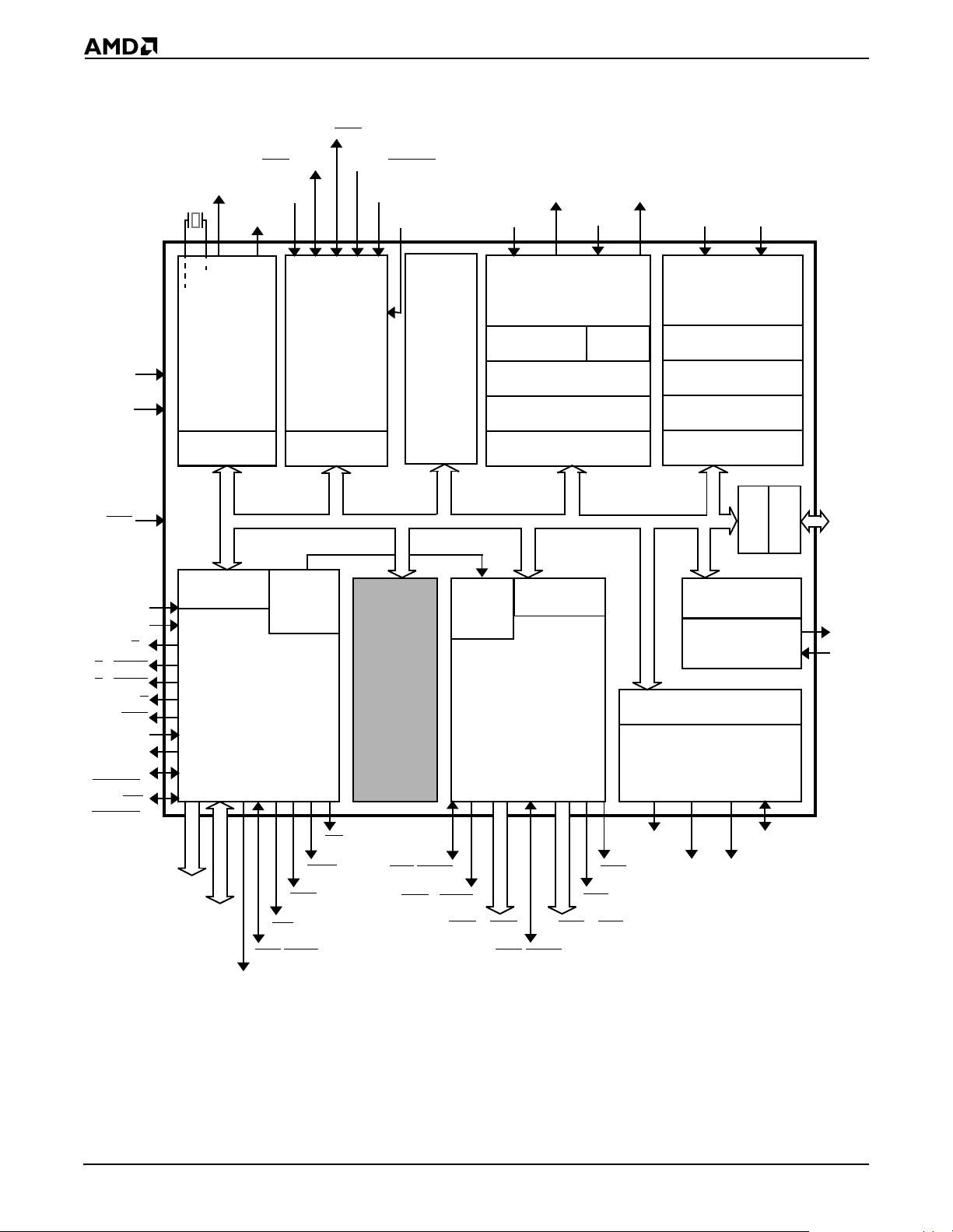
Figure 1-1 Am186ER Microcontroller Block Diagram
V
CC
GND
RES
ARDY
SRDY
S1/IMDIS
S0/SREN
DT/R
DEN
HOLD
HLDA
S6/
CLKSEL
UZI
CLKSEL
S2
1
/
2
INT3/INTA
CLKOUTA
CLKOUTB
X2
X1
Clock and
Power
Management
Unit
Control
Registers
Control
Registers
Interface
Bus
Unit
INT2/INTA
1/IRQ
INT4
Interrupt
Control Unit
Control
Registers
Refresh
Control
Unit
INT1/SELECT
RD
0
INT0
NMI
Execution
32 Kbyte
RAM
(16K x 16)
Unit
TMROUT0 TMROUT1
TMRIN0 TMRIN1
DRQ0 DRQ1
Timer Control
Unit
01 (WDT)2 0 1
Max Count B
20-Bit Source
Registers
Max Count A
20-Bit Destination
Registers
16-Bit Coun t
16-Bit Count
Registers
Control
Registers
PSRAM
Control
Unit
Control
Registers
Chip-Select
Unit
Asynchronous
Control
Registers
Synchronous Serial
Interface
SCLK
DMA
Unit
Pointers
Pointers
Registers
Control
Registers
Control
Control
Registers
Serial Port
SDATA
Unit
Registers
PIO
PIO31–
1
PIO0
TXD
RXD
1-4
A19–A0
AD15–AD0
ALE
BHE
WR
/ADEN
WLB
WHB
LCS/ONCE0
MCS3/RFSH
MCS
2–MCS0
UCS/ONCE1
PCS
PCS
5/A1
PCS
3–PCS0
6/A2
SDEN0 SDEN1
Notes:
1. All PIO signals are shared wi th other physic al pins. See the pin des criptions in Chapter 3 and
Table 3-1 on page 3-10 for information on shared functions.
Features and Performance
Page 19
Figure 1-2 Am188ER Microcontroller Block Diagram
INT2/INTA0
V
CC
GND
RES
ARDY
SRDY
S1/IMDIS
S0/SREN
DT/R
DEN
HOLD
HLDA
S6/
CLKSEL
UZI
CLKSEL
S2
1
/
2
A19–A0
CLKOUTA
X2
X1
Clock and
Power
Management
Unit
Control
Registers
Control
Registers
AO15–AO8
AD7–AD0
INT3/INTA
CLKOUTB
Bus
Interface
Unit
ALE
1/IRQ
INT4
Interrupt
Control Unit
Control
Registers
Refresh
Control
Unit
RD
WB
WR
RFSH2/ADEN
INT1/SELECT
INT0
NMI
Execution
32 Kbyte
RAM
(32K x 8)
LCS/ONCE0
MCS3/RFSH
Unit
MCS
TMROUT0 TMROUT1
TMRIN0 TMRIN1
Timer Control
01 (WDT)2 0 1
Max Count B
Registers
Max Count A
16-Bit Count
PSRAM
Control
Registers
Unit
Chip-Select
Unit
2–MCS0
UCS
/ONCE1
Unit
Registers
Registers
Control
Registers
Control
PCS
PCS
PCS
5/A1
3–PCS0
DRQ0 DRQ1
DMA
Unit
20-Bit Source
Pointers
20-Bit Destination
Pointers
16-Bit Count
Registers
Control
Registers
Control
Registers
Asynchronous
Serial Port
Control
Registers
Synchronous Serial
Interface
SCLK
SDEN0 SDEN1
6/A2
Control
Registers
SDATA
PIO
Unit
PIO31–
1
PIO0
TXD
RXD
Notes:
1. All PIO signals are shared wi th other physic al pins. See the pin des criptions in Chapter 3 and
Table 3-1 on page 3-10 for information on shared functions.
Features and Performance
1-5
Page 20
1.3 APPLICATION CONSIDERATIONS
The integration enhancements of the Am186ER and Am188ER microc ontrollers provide a
high-performance, low-syst em-cost solution for 16-bit embedded microcontrolle r designs.
The internal 32-Kbyte RAM allows t he manufacture of a complete embedded sy stem using
only one external ROM device and a low-cost crystal, plus any voltage conversion or current
drivers required for I/O. Internal RAM is enabled and configured by using the Internal
Memory Chip Select (IMCS) Register described in Chapter 6, “Internal Memory.”
The nonmultiplexed address bus (A19–A0) eliminates system-interface logic for external
memory, while the multi plexed address /data bus maint ains the value of existin g customerspecific peripherals and circuits within the upgraded design.
The nonmultiplexed address bus is available in additi on to the 80C186 and 80C188
microcontrollers’ multiplexed addres s/d ata bus (AD15–AD0). The two buses can operate
simultaneously, or the AD15–AD0 bus can be configured to operate only during the data
phase of a bus cycle. See the BHE
and see section 5 .5.1 an d sectio n 5.5.2 for a dditio nal in form ation regard ing the AD15 –AD0
address enabling and di sablin g.
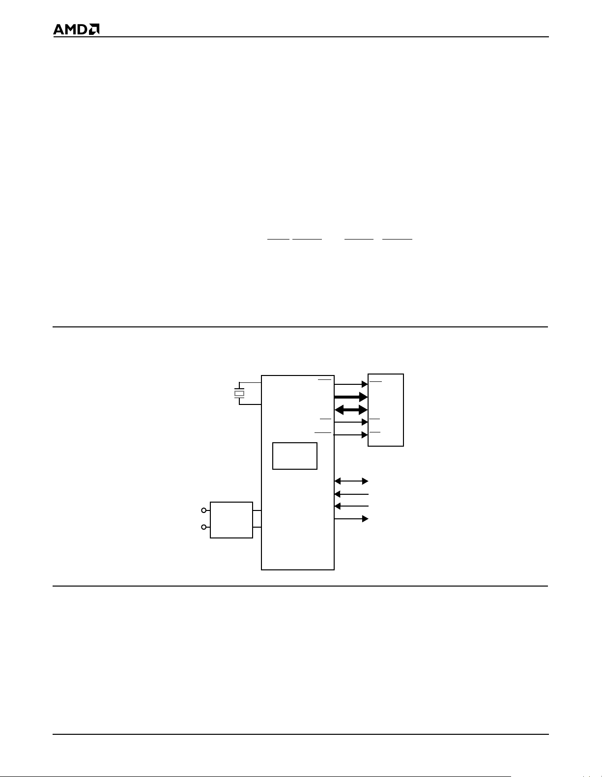
Figure 1-3 illustrates a functi onal sy stem de sig n tha t uses t he integ rat ed peri pheral se t t o
achieve high performance with reduced system cost.
/ADEN and RFSH2/ ADEN pin desc ription s in Chapt er 3,
Figure 1-3 Basic Functional System Design
Am186ER
Microcontroller
10-MHz
Crystal
Serial Port
RS-232
Level
Converter
X2
X1
32 Kbyte
RAM
TXD
RXD
1.3.1 Clock Generation
The integrated PLL clock-generation circuitry of the Am186ER and Am188ER
microcontrollers allows operation at one times or four times t he crystal frequency, in addition
to the one-half frequency operat ion required by 80C186 and 80C188 microc ontrollers. The
design in Figure 1-3 achieves 40-MHz CPU operation with a 10-MHz cryst al.
WR
A19–A0
AD15–AD0
RD
UCS
Timer 0–2
INT4–INT0
DMA 0–1
CLKOUTA
Am29F400
Flash
WE
Address
Data
OE
CS
40 MHz
1-6
The integrated PLL lowers system cost by reducing the cost of the crystal and reduces
electromagnetic interference (EMI ) in the system.
Features and Performance
Page 21

1.3.2 Memory Interface
The integrated memory controller logic of t he Am186ER and Am188ER microcontrollers
provides a direct address bus interface to memory devices. The use of an external address
latch controlled by the address latch enable (ALE) signal is not required.
Individual byte write-enable signals are provided to eliminate the need for external high/
low-byte, write-enable circuitr y. The maximum bank size programmable for the memory
chip-select signals is increased to 512 Kbyte to facil itate the use of high-density memory
devices.
Improved memory timing specifications enable the use of zero-wait-state memories with
70-ns access times at 40-MHz CPU operation. This reduces overall system cost
significantly by allowing the use of commonly available memory devices. The integrated
32-Kbyte RAM operates at the same speed as zero-wait-state external memory.
Figure 1-3 illustrates an Am186ER microcontroller-based configurati on with 512 Kbyte of
external Flash EPROM in addition to the internal 32-Kbyte memory. Addit ional external
RAM can also be added. The external memory interface requires the following:
n The processor A19–A0 bus connects to the memory address inputs.
n The AD bus connects directly to the data inputs/outputs.
n The UCS chip select connects to the memory chip-select input.
External read operations require that the RD
) input pin. External write operati ons require that the byte write enables con nect to the SRAM
(OE
Write Enable (WE
The example design shown in Figure 1-3 uses a 4-Mbit (256-K x 16) external Flash EPROM
for application memory, mapped into the upper region of the microcontroller’s 1-Mbyte
address space at 80000h–FFFFFh. After a valid reset, the Am186ER or Am188ER
microcontroller will fetch the first instruction from address FFFF0h. The user application
can then enable and configure the location of the integrated 32-Kbyte RAM within the
remaining address space ; in this example, it would be at address 00000h to accommodate
the interrupt vector table.
) input pin.
1.3.3 Seri al Communications Port
The integrated universal asynchronous receiver/transmitter (UART) controller in the
Am186ER and Am188ER microcontrollers eliminates the need for external logic to
implement a communications interface. The integrated UART generates the serial clock
from the CPU clock so that no external time-base oscillato r is r equir ed.
Figure 1-3 shows a minimal implementation of an RS-232 console or modem
communications port. The RS-232 to CMOS voltage-level converter is required for the
proper electrical interface with the external device.
The Am186ER and Am188ER microcontrollers al so include a synchronous serial interface.
For more information, see Chapter 11.
output connect s to t he SRAM Out put E nable
Features and Performance
1-7
Page 22

1.4 THIRD-PARTY DEVELOPMENT SUPPORT PRODUCTS
The FusionE86 Program of Partne rships for Applica tion Solut ions p rovid es the cus tomer w ith
an array of prod ucts design ed to meet cri tic al time- to-m arket needs . Produc ts a nd solut ions
available fro m the AMD Fusi onE86 pa rtn ers incl ude emu lators , hardw are and s oftwar e
debuggers, board-level products, and software development tools.
In addition, mature development tools and applications for the x86 platform are widely
available in the general marketplace.
1-8
Features and Performance
Page 23

CHAPTER
PROGRAMMING
2
All members of the Am186 and Am188 family of microcontr ollers, includi ng the Am186ER
and Am188ER, contain the same basic set of registers, instructions, and addressing modes,
and are compatible with the original industry-standard 186/188 parts.
2.1 REGISTER SET
The base architecture of the Am186ER and Am188ER microcontrollers has 14 registers,
as shown in Figure 2-1. These registers are grouped into the following categories:
n General Registers—Eight 16-bit general purpose registers ca n be used for arit hmetic
and logical operands. Four of these ( AX, BX, CX, and DX) can be used as 16-bit registers
or split into pairs of se parate 8-bit register s (AH, AL, BH, BL, CH, CL, DH, an d DL). The
Destination Index (DI) and Source Index (SI) general-purpose registers are used for
data movement and string instructions. The Base Point er (BP) and St ack Pointer (SP)
general-purpose register s are used for the stack segment and poi nt to the bottom and
top of the stack, respectively.
– Base and Index Registers—Four of the general-purpose registers (BP, BX, DI, and
SI) can also be used to determine offset addresses of operands in memory. These
registers can contain base addresses or indexes to part icular locations within a
segment. The addressing mode sel ects the specific registers for operand and addre ss
calculations.
– Stack Pointer Register—All stack operatio ns (POP, POPA, POPF, PUSH, PUSHA,
PUSHF) utilize the stack pointer. The Stack Pointer Register is always offset from the
Stack Segment (SS) Register, and no segment override is allowed.
n Segment Registers—Four 16-bit special-purpose registers (CS, DS, ES, and SS)
select, at any given time, the segments of memory that are immediately addressable
for code (CS), data (DS and ES), and stack (SS) memory. (For usage, refer to sectio n
2.2.)
n Status and Control Registers—Two 16-bit speci al-purpose registers record or alter certain
aspects of the processor state—the Instruction Pointer (IP) Register contains the offset
address of the ne xt s equenti al instru cti on to be ex ecut ed and th e Proc esso r Stat us Flags
(FLAGS) Register contains status and control flag bits (see Figure 2-1 and Figure 2-2).
Note that the Am186ER and Am188ER microcon trollers have additional on-chip per ipheral
registers, which are exter nal to the proc essor. These exter nal register s are not accessibl e
by the instruction set. However, because the processor t reat s these peripheral registers
like memory, instructions that have operands that access memory can also access
peripheral registers. The above processor registers, as well as the additional on-chip
peripheral registers, are described in the chapters that follow.
Programming
2-1
Page 24
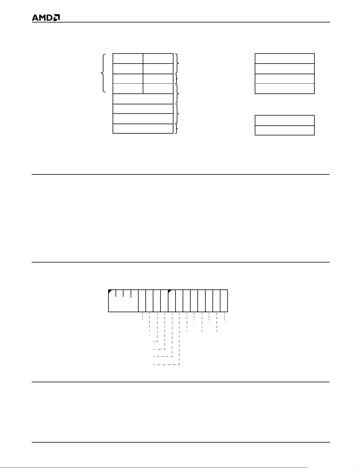
Figure 2-1 Register Set
16-Bit
Register Name
Byte
Addressable
(8-Bit
Register
Names
Shown)
7 0 7 0
AX
DX
CX
BX
BP
SI
DI
SP
AH
DH
CH
BH
Base Pointer
Source Index
Destination Index
15 0
General
Registers
AL
DL
CL
BL
Special Register
Functions
Multiply/Divide
I/O Instructions
Loop/Shift/Repeat/Count
Base Registers
Index Registers
Stack Pointer
2.1.1 Processor Status Flags Register
The 16-bit processor Status Flags Register ( Figure 2-2) reco rds specific c haracteristics of
the result of logical and arithmetic instructions (bits 0, 2, 4, 6, 7, and 11) and controls the
operation of the microcontroller within a given operating mode (bits 8, 9, and 10).
16-Bit
Register Name
FLAGS
15 0
CS
DS
SS
ES
Segment Registers
15 0
Processor Status Flags
IP
Instruction Pointer
Status and Control
Code Segment
Data Segment
Stack Segment
Extra Segment
Registers
After an instruction is ex ecuted, the va lue of the f lags may be set ( to 1), cl eared/reset (set
to 0), unchanged, or undefined. The term
execution of the instruction is not preserved, and the value of the flag after the instruction is
executed cannot be predi cted.
Figure 2-2 Processor Statu s Flags Registe r (FLAGS)
15
Reserved
OF
DF
IF
TF
SF
ZF
70
AF
Res
Bits 15–12—Reserved
undefined
PF
Res
Res
means that the fl ag va lue pri or to the
CF
2-2
Bit 11: Overflow Flag (OF)—Set if the signed result cannot be expressed within the number
of bits in the destination operand; cleared o ther wise.
Bit 10: Direction Flag (DF)—Causes string instructions to auto-decrement the appropriate
index registers when set. Clearing DF causes auto-increment.
Programming
Page 25

Bit 9: Interrupt-Enable Flag (IF)—When set, enables maskable interrupts to cause the
CPU to transfer control to a location specified by an interrupt vector .
Bit 8: Trace Flag (TF)—When set, a trace interrupt occurs after instructions execute. TF
is cleared by the t race interr upt after t he processor st atus flags are pushed onto t he stack.
The trace service routine can continue t racing by poppi ng the fl ags back with an int errupt
return (IRET) instruct ion.
Bit 7: Sign Flag (SF)—Set equal to h igh-order bit of r esult (0 if 0 or positive, 1 if negative).
Bit 6: Zero Flag (ZF)—Set if result is 0; clear ed otherwise.
Bit 5: Reserved
Bit 4: Auxiliary Carry (AF)—Set on carry f rom or borrow to the low-or der 4 bits of the AL
general-purpose register; cleared otherwise.
Bit 3: Reserved
Bit 2: Parity Flag (PF)—Set if low-order 8 bi ts of resul t contain an ev en number of 1 bits;
cleared otherwise.
Bit 1: Reserved
Bit 0: Carry Flag (CF)—Set on high-order bit carry or borrow; cleared otherwise.
2.2 MEMORY ORGANIZATION AND ADDRESS GENERATION
Memory is organized in sets of segments. Each segment is a linear contiguous sequence
of 64K (2
of a 16-bit segment value and a 16-bit offset. The offset is the number of bytes from the
beginning of the segment (the segment address) to the data or instruction that is being
accessed.
16
) 8-bit bytes. Memory is addressed using a two-component address that consists
The processor forms the physical address of the target location by taking the segment
address, shifting it to the left 4 bits (multi plying by 16), and adding this to the 16-b it offset.
The result is the 20-bit address of the target data or instruction. This allows for a 1-Mbyte
physical address size.
For example, if the segment register is loaded with 12A4h and the offset i s 0022h, the
resultant address is 12A62h (see Figure 2-3). To find the result:
1. The segment register contains 12A4h.
2. The segment register is shifted left 4 places and is now 12A40h.
3. The offset is 0022h.
4. The shifted segment address (12A40h) is added to the offset (00022h) to get 12A62h.
5. This address is placed on the pins of the controller.
All instructions that address operands in memory must specify (implicitly or explicitly) a
16-bit segment value and a 16-bit of fset value. The 16-bit segment values a re con tained i n
one of four int er na l s eg me nt r egi st e rs ( C S, DS , ES , an d SS) . See “Add ress ing Modes” on
page 2-10 for more information on calculating the offset value. See “Segments” on page
2-8 for more information on CS, DS, ES, and SS.
In addition to memory space, all Am186 and Am188 family microcontrollers provide 64K
of I/O space (see Figure 2-4).
Programming
2-3
Page 26
Figure 2-3 Physical Address Generatio n
Shift
Left
4 Bits
1 2 A 4 0
19 0
0 0 0 2 2
15 0
1 2 A 4
15 0
15
0 0 2 2
Segment
Base
Offset
0
Logical
Address
1 2 A 6 2
19 0
To Memory
2.3 I/O SPACE
The I/O space consists of 64K 8-bit or 32K 16-bit port s. The IN and OUT instructions address
the I/O space with either an 8-bit port addr ess specified in the instruction, or a 16-bit port
address in the DX Register. Eight-bit port addresses are zero-extended so that A15–A8
are Low. I/O port addresses 00F8h through 00FFh are reserved. The Am186ER and
Am188ER microcontrollers provide specific instructions for addressing I/O space.
Figure 2-4 Memory an d I/O Space
Memory
Space
1M
I/O
Space
Physical Address
64K
2.4 INSTRUCTION SET
The Am186ER and Am188ER microcontrollers use the same instruction set as the 80C186
microcontroller. An instruct ion can reference from zero to several operands. An operand
can reside in a register , in the inst ruction itself, or in memory. Specif ic operand addressi ng
modes are discussed on page 2-10.
Table 2-1 lists the instructions for the Am1 86ER and Am188ER microcont rollers in
alphabetical order.
#21267, provides detailed information on the format and function of the following
instructions.
2-4
The Am186™ and Am188™ Family Instruction Set Manual
, order
Programming
Page 27

Table 2-1 Instruction Set
Mnemonic Instruction Name
AAA ASCII adjust for addition
AAD ASCII adjust for division
AAM ASCII adjust for multiplication
AAS ASCII adjust for subtraction
ADC Add byte or word with carry
ADD Add byte or word
AND Logical AND byte or word
BOUND Detects values outside prescribed range
CALL Call procedure
CBW Convert byte to word
CLC Clear carry flag
CLD Clear direction flag
CLI Clear interrupt-enable flag
CMC Complement carry flag
CMP Compare byte or word
CMPS Compare byte or word string
CWD Convert word to doubleword
DAA Decimal adjust for addition
DAS Decimal adjust for subtraction
DEC Decrement byte or word by 1
DIV Divide byte or word unsigned
ENTER Format stack for procedure entry
ESC Escape to extension processor
HLT Halt until interrupt or reset
IDIV Integer divide byte or word
IMUL Integer multiply byte or word
IN Input byte or word
INC Increment byte or word by 1
INS Input bytes or word string
INT Interrupt
INTO Interrupt if overflow
IRET Interrupt return
JA/JNBE Jump if above/not below or equal
JAE/JNB Jump if above or equal/not below
Programming
2-5
Page 28

Mnemonic Instruction Name
JB/JNAE Jump if below/not above or equal
JBE/JNA Jump if below or equal/not above
JC Jump if carry
JCXZ Jump if register CX = 0
JE/JZ Jump if equal/zero
JG/JNLE Jump if greater/not less or equal
JGE/JNL Jump if greater or equal/not less
JL/JNGE Jump if less/not greater or equal
JLE/JNG Jump if less or equal/not greater
JMP Jump
JNC Jump if not carry
JNE/JNZ Jump if not equal/not zero
JNO Jump if not overflow
JNP/JPO Jump if not parity/parity odd
JNS Jump if not sign
JO Jump if overflow
JP/JPE Jump if parity/parity even
JS Jump if sign
LAHF Load AH register from flags
LDS Load pointer using DS
LEA Load effective address
LEAVE Restore stack for procedure exit
LES Load pointer using ES
LOCK Lock bus during next instruction
LODS Load byte or word string
LOOP Loop
LOOPE/
LOOPZ
LOOPNE/
LOOPNZ
MOV Move byte or word
Loop if equal/zero
Loop if not equal/not zero
2-6
MOVS Move byte or word string
MUL Multiply byte or word unsigned
NEG Negate byte or word
NOP No operation
NOT Logical NOT byte or word
Programming
Page 29

Mnemonic Instruction Name
OR Logical inclusive OR byte or word
OUT Output byte or word
POP Pop word off stack
POPA Pop all general register off stack
POPF Pop flags off stack
PUSH Push word onto stack
PUSHA Push all general registers onto stack
PUSHF Push flags onto stack
RCL Rotate left through carry byte or word
RCR Rotate right through carry byte or word
REP Repeat
REPE/REPZ Repeat while equal/zero
REPNE/
REPNZ
RET0 Return from procedure
ROL Rotate left byte or word
ROR Rotate right byte or word
SAHF Store AH register in flags SF, ZF, AF, PF, and CF
SAL Shift left arithmetic byte or word
SAR Shift right arithmetic byte or word
SBB Subtract byte or word with borrow
SCAS Scan byte or word string
SHL Shift left logical byte or word
SHR Shift right logical byte or word
STC Set carry flag
STD Set direction flag
STI Set interrupt-enable flag
STOS Store byte or word string
Repeat while not equal/not zero
SUB Subtract byte or word
TEST Test (logical AND, flags only set) byte or word
XCHG Exchange byte or word
XLAT Translate byte
XOR Logical exclusive OR byte or word
Programming
2-7
Page 30
2.5 SEGMENTS
The Am186ER and Am188ER microcontrollers use four segment registers:
1. Data Segment (DS): The processor assumes that all accesses to the program’s
variables are from the 64K space pointed to by the DS Register. The data segment holds
data, operands, etc.
2. Code Segment (CS): This 64K space is the default locati on for all instruct ions. All code
must be executed from the code segment.
3. Stack Segment (SS): The processor uses the SS Register to perform operations that
involve the stack, such as pushes and pops. The st ack segment i s used for t emporar y
space.
4. Extra Segment (ES): Usually this segment is used for large string operati ons and for
large data structures. Certain str ing i n structions assume the extra segment as the
segment portion of the address. The extra segment is also used (by using segment
override) as a spare data segment.
When a segment is not defined for a data movement instruc tion, it’s assumed to be a data
segment. An instruction prefix can be used to override the segment register. For speed
and compact instruction encoding, the segment register used for physical address
generation is implied by the addressing mode used (see Table 2-2).
Table 2-2 Segment Regist er Selection Rules
Memory Reference
Needed
Local Data Data (DS) All data references
Instructions Code (CS) Instructions (including immedi ate data)
Stack Stack (SS) All stack pushes and pops
External Data (Global) Extra (ES) All string instruc tion references that use the DI Regi s-
Segment Register
Used
2.6 DATA TYPES
The Am186ER and Am188ER microcontrollers directly support the following data types:
n Integer—A signed binary numeric value contained in an 8-bit byte or a 16-bit word. All
operations assume a two’s complement representation.
n Ordinal—An unsigned binary numeric value contained in an 8-bit byt e or a 16-bit wor d.
n Double Word—A signed binary numeric value contained in two sequential 16-bit
addresses, or in a DX::AX register pair.
n Quad Word—A signed binary numeric value contained in four sequential 16-bit
addresses.
Implicit Segment Selection Rule
Any memory references that use the BP Reg ister
ter as an index
2-8
n Binary-Coded Decimal (BCD)—An unpacked byte representation of the decimal
digits 0–9.
n ASCII—A byte representation of alphanumeric and c ontr ol char acters usi ng the ASCII
standard of character representation.
n Packed BCD—A packed byte representation of two decimal digits (0–9). One digit is
stored in each nibble (4 bits) of the byte.
Programming
Page 31

n String—A contiguous sequence of bytes or words. A string can contain fr om 1 byte up
to 64 Kbyte.
n Pointer—A 16-bit or 32-bit quantity, composed of a 16-bi t offset component or a 16-bi t
segment base component plus a 16-bit offset component.
In general, individual data elements must fit within defined segment limits. Figure 2-5
graphically represents the data types supported by the Am186ER and Am188ER
microcontrollers.
Figure 2-5 Supported Data Types
Signed
Byte
Sign Bit
Unsigned
Byte
Signed
Word
Sign Bit
Signed
Double
Word
Sign Bit
Signed
Quad
Word
Sign Bit
Unsigned
Word
7 0
Magnitude
7 0
MSB
Magnitude
+1 0
1514 8 7 0
MSB
Magnitude
+3
31 1615 0
+2
+1 0
MSB
Magnitude
63 48 47 32 31 1615 0
+3 +2 +1+6 +5 +4 +0+7
MSB
Magnitude
+1 0
015
MSB
Magnitude
Binary
Coded
Decimal
(BCD)
ASCII
Packed
BCD
String
Pointer
+N +1 0
7 0 7 0 7 0
BCD
Digit N
7 0 7 0 7 0
. . .
BCD
Digit 1
+N +1 0
BCD
Digit 0
. . .
ASCII
Character
7 0 7 0 7 0
N
+N +1 0
ASCII
Character
ASCII
Character
1
0
. . .
Most Significant
Digit
+N
70
. . .
Significant Digit
+1 0
7 0 7 0
Least
Byte/WordN Byte/Word1 Byte/Word0
+3 +2 +1 0
Segment Base Offset
Programming
2-9
Page 32

2.7 ADDRESSING MODES
The Am186ER and Am188ER microcontrollers u se eight categori es of addressing modes
to specify operands. Two addressing modes are provided for i nstruct ions that operate o n
register or immediate operands; six modes are provided to specify the location of an
operand in a memory segment.
Register and Immediate Operands
n Register Operand Mode—The operand is located in one of the 8- or 16-bit registers.
n Immediate Operand Mode—The operand is included in the instruction.
Memory Operands
A memory-operand address consists of two 16-bit components: a segment value and an
offset. The segment value is supplied by a 16-bit segme nt register either i mplicitly chosen
by the addressing mode or e xplicitly chosen by a segment override pref ix. The off set, also
called the effective address, is calculated by summing any combination of the following
three address elements:
1. Displacement—an 8-bit or 16-bit imme diate value co ntain ed in the i nstru ctio n
2. Base—contents of either the BX or BP ba se re giste rs
3. Index—contents of either the SI or DI ind ex regi sters
Any carry from the 16-bit addition is ignored. Eight-bit displacements ar e sign-extended to
16-bit values.
Combinations of the above three address elements define the following six memory
addressing modes (see Table 2-3):
1. Direct Mode—The operand offset is cont ained in the i nstr uctio n as an 8- o r 16-bit
displacement element.
2. Register Indirect Mode—The operand offset is in one of the registers: SI, DI, BX, or BP.
3. Based Mode—The operand offset is the sum of an 8- or 16-bit displacement and the contents
of a base regist er (BX or BP).
4. Indexed Mode—The operand offset is the su m of an 8- o r 16-bit displa cement and the
contents of an index register (SI or DI).
5. Based Indexed Mode—The operand offset is t he sum of the cont ents of a base r egist er
(BX or BP) and an index register (SI or DI).
6. Based Indexed Mode with Displacement—The operand offs et is the s um of a base
register’s conten ts, an index regis ter’ s conte nts, an d an 8- bit or 16-b it disp lac ement .
Table 2-3 Memory Addressing Mode Examples
Addressing Mode Example
Direct mov ax, ds:4
Register Indirect mov ax, [si]
Based mov ax, [bx]4
Indexed mov ax, [si]4
Based Indexed mov ax, [si][bx]
Based Indexed with Displacement mov ax, [si][bx]4
2-10
Programming
Page 33

CHAPTER
SYSTEM OVERVIEW
3
This chapter contains descriptions of the Am186ER and Am188ER microcontro ller pins,
the bus interface unit, the clock and p ower management unit, and the power-save operation.
3.1 PIN DESCRIPTIONS
Pin Terminology
The following terms are used to describe the pins:
Input—An input-only pin.
Output—An output-only pin.
Input/Output—A pin that can be either input or output.
Synchronous—Synchronous inputs must meet setup and hold times in relation to
CLKOUTA. Synchronous outputs are synchronous to CLKOUTA.
Asynchronous—Inputs or outputs that are asynchronous to CLKOUTA.
A19–A0 Address Bus (output, three-state, synchronous)
The A19–A0 pins supply nonmultiplexed memory or I/O addresses to
the system one-half of a CLKOUTA period earlier than the multiplexed
address and data bus (AD15–AD0 on the Am186ER microcontro ller or
AO15–AO8 and AD7–AD0 on the Am188ER microcontroller). Durin g a
bus hold or reset condition, the address bus is in a high-impedance
state.
AD7–AD0 Address and Data Bus
(input/output, three-state, synchronous, level-sensitive)
These time-multiplexed pins supply partial memory or I/O addresses,
as well as data, to the system. AD7–AD0 supply the l ow-order 8 bits of
an address to the system duri ng th e fir st pe riod of a bus cyc le (t
a write, these pins supply data to the system during the remaining
periods of that cycle (t
the end of t
Also, if S0
the SR bit is set in the Internal Memory Chip Select (IMCS) Register,
these pins supply the data read from internal memory during t
On the Am186ER microcontroller , AD7–AD0 combine with AD15–AD8
to form a complete multiplexed address and 16-bit data bus.
.
3
/SREN (show read enable) was pulled Low during re set or if
, t3, and t4). On a read, these pins latch data at
2
). On
1
and t4.
3
On the Am188ER microcontroller , AD7–AD0 combine with AO15–AO8
to form a complete multiplexed addr ess bus while AD7–AD0 is the 8-bit
data bus.
System Overview
3-1
Page 34

The address phase of these pins can be disabled. See the ADEN
description with the BHE
pins are three-stated during t
/ADEN pin. When WLB is not asserted, these
, t3, and t4.
2
During a bus hold or reset condition, the address and data bus is in a
high-impedance state.
During a power-on reset, the address and data bus pins (AD15–AD0
for the Am186ER microcontroller, AO15–AO8 and AD7–AD0 for the
Am188ER microcontroller) can also be used to load system
configuration information into the internal Reset Configuration Register .
The system information is latched on the rising edge of RES.
AD15–AD8 Address and Data Bus, Am186ER Microcontroller Only
(input/output, three-state, synchronous, level-sensitive)
These time-multiplexed pins supply partial memory or I/O addresses,
as well as data, to the system. AD15–AD8 supply the high-order 8 bit s
of an address to the system during the first period of a bus cycle (t
On a write, these pins supply data to the system during the remaining
periods of that cycle (t
the end of t
.
3
, t3, and t4). On a read, these pins latch data at
2
).
1
Also, if S0
/SREN (show read enable) was pulled Low during re set or if
the SR bit is set in the Internal Memory Chip Select (IMCS) Register,
these pins supply the data read from internal memory during t
On the Am186ER microcontroller , AD15–AD8 combine with AD7–AD0
to form a complete multiplexed address and 16-bit data bus.
The address phase of these pins can be disabled. See the ADEN
description with th e BHE
pins are three-stated during t
/ADEN pin. When WHB is not asserted, these
, t3, and t4.
2
During a bus hold or reset condition, the address and data bus is in a
high-impedance state. During a power- on reset, th e address and da ta
bus pins (AD15–AD0 for the Am186ER microcont roller, AO15–AO8 and
AD7–AD0 for the Am188ER microcontroller) can also be used to load
system configuration information into the inter nal Reset Configuration
Register . The system infor mation is latched on the r ising edge of RES.
AO15–AO8 Address-Only Bus, Am188ER Microcontroller Only
(output, three-state, synchronous, level-sensitive)
The address-only bus (AO15–AO8) contai ns v alid h igh-ord er addres s
bits from bus cycles t
. These outputs are three-stated during a bus
1–t4
hold or reset.
On the Am188ER microcontroller , AO15–AO8 combine with AD7–AD0
to form a complete multiplexed addr ess bus while AD7–AD0 is the 8-bit
data bus.
and t4.
3
3-2
During a power-on reset on the Am188ER microcontroller, the AO15–
AO8 and AD7–AD0 pins can also be used to load system configuration
information into an internal register for later use.
ALE Address Latch Enable (output, synchronous)
This pin indicates to the system that an address appears on the address
and data bus (AD15–AD0 for the Am186ER microcontroller or AO15–
System Overview
Page 35

AO8 and AD7–AD0 for the Am188ER microcontroller). The address i s
guaranteed to be valid on the trailing edge of ALE. This pin is thr eestated during ONCE mode.
ARDY Asynchronous Ready (input, asynchronous, level-sensitive)
This pin indicates to the microcontroller that the addressed memory
space or I/O device will complete a data transfer. The ARDY pin accepts
a rising edge that is asynchronous to CLKOUT A and is active High. The
falling edge of ARDY must be synchronized to CLKOUTA. To always
assert the ready condition to the microc ontroller, tie ARDY High. If the
system does not use ARDY, tie the pin Low to yield control to SRDY.
/ADEN Bus High Enable, Am186ER Microcontroller Only
BHE
(three-state, output, synchronous)
Address Enable, Am186ER Microcontroller Only
(input, internal pullup)
—During a memory access, this pin and the least significant
BHE
address bit (AD0 and A0) indic ate to the system which bytes of the data
bus (upper, lower, or both) participate in a bus cycle. The BHE
/ADEN
and AD0 pins are encoded as shown in the following table.
BHE/ADEN AD0 Type of Bus Cycle
0 0 Word Transfer
01High Byte Transfer (Bits 15–8)
1 0 Low Byte Transfer (Bits 7–0)
11Refresh
is asserted during t1 and remains asserted through t3 and tW. BHE
BHE
does not need to be latched. BHE
is three-stated during bus hold and
reset conditions.
On the Am186ER microcontroller, WLB
functionality of BHE
BHE
/ADEN also signals DRAM refresh cycles when using the
and AD0 for high and low byt e write en able s.
and WHB implement the
multiplexed address and data (AD) bus. A refresh cycle is indi cated
when both BHE
/ADEN and AD0 are High. During r efresh cycles, the A
bus and the AD bus are not guaranteed to provide the same address
during the address phase of the AD bus cycle. For this reas on, the A0
signal cannot be used in place of the AD0 signal to determine refresh
cycles. PSRAM refreshes also provide an additional RFSH
the MCS
ADEN
3/RFSH pin description).
—If BHE/ADEN is held High or le ft three-stated dur ing power-on
signal (see
reset, the address portion of the AD bus (AD15–AD0) is enabled or
disabled during LCS
and UCS bus cycles based on the DA bit in the
Upper Memory Chip Select (UMCS) and Low Memory Chip Select
(LMCS) registers. If the DA bit is set, the memory address is accessed
on the A19–A0 pins. This mode of operation reduces power
consumption.
If BHE
/ADEN is held Low on power-on reset , the AD bus always driv es
both addresses and data. (S6 and UZI also assume their normal
System Overview
3-3
Page 36

functionality in this instance. See Table 3-1 on page 3-10.) The pin is
sampled within three c rystal cloc k c ycles after t he ris ing edge of RE
BHE/ADEN is three-stated during bus holds and ONCE mode.
See section 5.5.1 and section 5.5.2 for additi onal information on
enabling and disabling the AD bus duri ng the address phase of a bus
cycle.
CLKOUTA Clock Output A (output, synchronous)
This pin supplies the internal clock to the system. Depending on the
value of the Power-Save Control (PDCON) Register, CLKOUTA
operates at either the CPU fundamental clock frequency (which var ies
with the Divide By Two, Times One, and T i mes Four cl ocking modes ),
the power-save frequency , or is three-stated. CLKOUT A remains active
during reset and bus hold conditions.
CLKOUTB Clock Output B (output, synchronous)
This pin supplies an addi tional clock to the system. Depending on the
value of the Power-Save Control (PDCON) Register, CLKOUTB
operates at either the CPU fundamental clock frequency (which var ies
with the Divide By Two, Times One, and T i mes Four cl ocking modes ),
the power-save frequency , or is thr ee-stated. CLKOUTB remains active
during reset and bus hold conditions.
S.
DEN
Data Enable (output, three-state, synchronous)
This pin supplies an output enabl e to an external data- bus transceiver .
DEN
is asserted during memory , I/O, and in terrupt acknowledge cycles.
is deasserted when DT/R changes state. DEN is three-stated
DEN
during a bus hold or reset condition.
DRQ1–DRQ0 DMA Requests (input, synchronous, level-sensitive)
These pins indicate to the microcontroller that an external device is
ready for DMA channel 1 or channel 0 to perform a transfer. DRQ1–
DRQ0 are level-triggered and internally synchronized.
The DRQ signals are not latched and must remain active until service d.
DT/R
Data Transmit or Receive (output, three-state, synchronous)
This pin indicates whic h direction data should f low through an external
data-bus transceiver . When DT/R
is asserted High, the microcontroller
transmits data. When this pin is deasserted Low, the microcontroller
receives data. DT/R
is three-stated during a bus hold or reset condit ion.
GND Ground
These pins connect the system ground to the microcontroller.
HLDA Bus Hold Acknowledge (output, synchronous)
3-4
When an external bus master requests control of the local bus (by
asserting HOLD), the microcontroller completes the bus cycle in
progress and then relinquishes control of the bus to the external bus
master by asserting HLDA and three-stating DEN
AD15–AD0, S6, A19–A0, BHE
the chip selects UCS
0 High.
PCS
System Overview
, LCS, MCS3–MCS0, PCS6–PCS5, and PCS3–
, WHB, WLB, and DT/R, and then driving
, RD, WR, S2–S0,
Page 37

When the external bus master has finished using the local bus, it
indicates this to the microcontrol ler b y deasserting HOLD. The
microcontroller responds by deasserti ng HLDA.
If the microcontroller requi res access to the bus (e.g., f or refresh), it will
deassert HLDA before the external bus mas ter deasserts HOLD. The
external bus master must be able to deassert HOLD and allow the
microcontroller access to the bus.
HOLD Bus Hold Request (input, synchronous, level-sensitive)
This pin indicates to the microcontroller that an external bus master
needs control of the local bus. For more information, see the HLDA pin
description.
The Am186ER and Am188ER microcontrollers ’ HOLD latency time, the
time between HOLD request and HOLD acknowledge, is a functi on of
the activity occurring in the processor when the HOLD request is
received. A HOLD request is second only to DRAM refresh requests in
priority of activi ty requests received by t he processor. This implies that
if a HOLD request is received just as a DMA transfer begins, the HOLD
latency can be as great as four bus cycles. This occurs if a DMA word
transfer operation is taking place (Am186ER microcontroller on ly) from
an odd address to an odd address. This is a total of 16 clock cycl es or
more if wait states are required. In addition, if locked tr ansfers are
performed, the HOLD latency time is increased by the length of the
locked transfer.
INT0 Maskable Interrupt Request 0 (input, asynchronous)
This pin indicates to the microcontroller that an interrupt request has
occurred. If the INT0 pin is not masked, the microcontroller transfers
program execution to the location specified by the INT0 vector in the
microcontroller interrupt vector table.
Interrupt requests are synchronized internally and can be edgetriggered or level-triggere d. To guarantee the interr upt is recognized,
the device issuing the request must continue asserting INT0 until the
request is acknowledged.
INT1/SELECT
Maskable Interrupt Request 1 (input, asynchronous)
Slave Select (input, asynchronous)
INT1—This pin indicates to the microcontroller that an interr upt request
has occurred. If the INT1 pin is not maske d, the microcontroller transfers
program execution to the location specified by the INT1 vector in the
microcontroller interrupt vector table.
Interrupt requests are synchronized internally, and can be edgetriggered or level-triggere d. To guarantee the interr upt is recognized,
the device issuing the request must continue asserting INT1 until the
request is acknowledged.
SELECT
—When the microcontroller interrupt control unit is operating
as a slave to an external master interrupt controller, this pin indicates
to the microcontroller tha t an interrupt type appears on the address and
data bus. The INT0 pin must indicate to the microcontroller that an
interrupt has occurred before the SELECT
pin indicates to the
microcontroller that the interrupt type appears on the bus.
System Overview
3-5
Page 38

INT2/INTA0 Maskable Interrupt Request 2 (input, asynchronous)
Interrupt Acknowledge 0 (output, synchronous)
INT2—This pin indicates to the microcontroller that an interr upt request
has occurred. If the INT2 pin is not maske d, the microcontroller transfers
program execution to the location specified by the INT2 vector in the
microcontroller interrupt vector table.
Interrupt requests are synchronized internally and can be edgetriggered or level-triggere d. To guarantee the interr upt is recognized,
the device issuing the request must continue asserting INT2 until the
request is acknowledged. INT2 becomes INTA
0 when INT0 is
configured in Cascade mode.
INT A
0—When the microcontroller interrupt control unit is operating in
Cascade mode, this pin indicat es to the system that th e microcontroller
needs an interrupt type to process the interrupt request on INT0. The
peripheral issuing the interrupt request must provide the microcontroller
with the corresponding interrupt type.
INT3/INTA
1/IRQ Maskable Interrupt Request 3 (input, asynchronous)
Interrupt Acknowledge 1 (output, synchronous)
Slave Interrupt Request (output, synchronous)
INT3—This pin indicates to the microcontroller that an interr upt request
has occurred. If the INT3 pin is not masked, the microcontroller then
transfers program execution to th e location specified by the INT3 vector
in the microcontroller interrupt vector table.
Interrupt requests are synchronized internally and can be edgetriggered or level-triggere d. To guarantee the interr upt is recognized,
the device issuing the request must continue asserting INT3 until the
request is acknowledged. INT3 becomes INTA
1 when INT1 is
configured in Cascade mode.
INT A
1—When the microcontroller interrupt control unit is operating in
Cascade mode, this pin indicat es to the system that th e microcontroller
needs an interrupt type to process the interrupt request on INT1. The
peripheral issuing the interrupt request must provide the microcontroller
with the corresponding interrupt type.
IRQ—When the microcontroller interrupt control unit is operating as a
slave to an external master interrupt controller, this pin let s the
microcontroller issue an interrupt request to the external master
interrupt controller.
3-6
INT4 Maskable Interrupt Request 4 (input, asynchronous)
This pin indicates to the microcontroller that an interrupt request has
occurred. If the INT4 pin is not masked, the microcontroller then
transfers program execution to th e location specified by the INT4 vector
in the microcontroller interrupt vector table.
Interrupt requests are synchronized internally and can be edgetriggered or level-triggere d. To guarantee the interr upt is recognized,
the device issuing the request must continue asserting INT4 until the
request is acknowledged.
System Overview
Page 39

LCS/ONCE0 Lower Memory Chip Select (output, synchronous, internal pullup)
ONCE Mode Request 0 (input)
LCS
—This pin indicates to the system that a memory access is in
progress to the lower memory block. The size of the lower memory
block is programmable up to 512 Kby te. LCS
is held High during a bus
hold condition.
ONCE
0—During reset, this pin and UCS/ONCE1 indicate to the
microcontroller the mode in which it should operate. ONCE
ONCE
1 are sampled on the rising edge of RES. If both pins are asserted
Low, the microcontroller enters ONCE mode; otherwise, it operates
normally.
In ONCE mode, all pins assume a high-impedance state and r emain in
that state until a subsequent reset occurs. To guarantee that the
microcontroller does not inadvertently enter ONCE mode, ONCE
a weak internal pullup resistor that is active only during a reset.
MCS
3/RFSH Midrange Memory Chip Select 3
(output, synchronous, internal pullup)
Automatic Refresh (output, synchronous)
3—This pin indicates to the system that a memory access is in
MCS
progress to the fourth regi on of the midran ge memory block. The ba se
address and size of the midrange memory block are programmable.
3 is held High during a bus hold condition. In addition, thi s pin has
MCS
a weak internal pullup resistor that is active during reset.
RFSH
—This pin provides a signal timed for auto refresh to PSRAM
devices. It is only enabled to function as a refr esh pulse when the
PSRAM mode bit is set in the LMCS Register . An active Low pulse is
generated for 1.5 clock cycl es wit h an adequate dea sser tion per iod t o
ensure that overall auto refr esh cycle time is met.
0 and
0 has
2–MCS0 Midrange Memory Chip Selects
MCS
(output, synchronous, internal pullup)
These pins indicate to the system that a memory access is in progress
to the corresponding region of the midrange memory block. The base
address and size of the midrange memory block are programmable.
2–MCS0 are held High during a bus hold condition. In addition,
MCS
they have weak internal pullup resistors th at are active during a reset.
Unlike the UCS
and LCS chip selects, t he MCS outputs assert with the
multiplexed AD address bus.
NMI Nonmaskable Interrupt (input, synchronous, edge-sensitive)
This pin indicates to the microcontroller that an interrupt request has
occurred. The NMI signal is the highest prio rity hardware interr upt and,
unlike the INT4–INT0 pins, cannot be masked. The microcontroller
always transfers program execution to the locati on specified by the
nonmaskable interrupt vector in the microcontroller interrupt vector
table when NMI is asserted.
Although NMI is the highest priority interrupt source, it does not
participate in the priority resolu tion process of the maskable interrupts.
There is no bit associat ed with NMI in the interrupt in-service or interrupt
request registers. This means that a new NMI request can int errupt an
System Overview
3-7
Page 40

executing NMI interrupt servi ce routine. As with all hardware interr upts,
the IF (interrupt flag) is cleared when the process or takes the interrupt,
disabling the maskable interrupt sources. However, if maskable
interrupts are re-enabled by sof tware in the NMI interrupt service routine
(via the STI instruction for example), the fa ct that an NMI is curren tly in
service will not have any effe ct on the priority resolution of maskable
interrupt requests. For this reason, it is strongly advised that the interrupt
service routine for NMI does not enable the maskable inter rupts.
An NMI transition from Low to High is latched and synchronized
internally, and it initiates the interrupt at the next instru ction bounda ry.
To guarantee that the interrupt is recognized, the NMI pin must be
asserted for at leas t one CLKOUT A period. Becaus e NMI is rising edge
sensitive, holding the pin High during reset has no effect on program
execution.
3–PCS0 Peripheral Chip Selects (output, synchronous)
PCS
These pins indicate to the system that a memory access is in progress
to the corresponding region of the peripheral memory block (either I/O
or memory address space). The base address of the peripheral memory
block is programmable. PCS
3–PCS0 are held High during a bus hold
or reset condition.
Unlike the UCS
and LCS chip selects, th e PCS outputs assert with the
multiplexed AD address bus.
Note: PCS
4 is not available on the Am186ER and Am188ER
microcontrollers. Note also that each peripheral chip select asserts over
a 256-byte address range, which is twice the address range covered by
peripheral chip selects in the 80C186 and 80C188 microcontrollers.
5/A1 Peripheral Chip Select 5 (output, synchronous)
PCS
Latched Address Bit 1 (output, synchronous)
PCS
5—This pin indicates to the system that a memory access is in
progress to the sixth region of the periphera l memory block (eithe r I/O
or memory address space). The base address of the peripheral memory
block is programmable. PCS
5 is held High during a bus hold or reset
condition. It is also held High during reset.
Note: Unlike the UCS
and LCS chip selects, the PCS outputs assert
with the multiplexed AD address bus. Note also that each peripheral
chip select asserts over a 256-byte address range, which is t wice the
address range covered by peripheral chip selects in the 80C186 and
80C188 microcontrollers.
A1—When the EX bit in the MCS
and PCS Auxiliary Register is 0, this
pin supplies an internall y latched address bi t 1 to the system. Duri ng a
bus hold condition, A1 retains its previou sly latched value.
3-8
6/A2 Peripheral Chip Select 6 (output, synchronous)
PCS
Latched Address Bit 2 (output, synchronous)
PCS
6—This pin indicates to the system that a memory access is in
progress to the seventh region of the peripheral memory block (either
I/O or memory address space). The base address of the peripheral
memory block is programmable. PCS
6 is held High during a bus hold
or reset condition.
System Overview
Page 41

Note: Unlike the UCS and LCS chip selects, the PCS outputs assert
with the multiplexed AD address bus. Note also that each peripheral
chip select asserts over a 256-byte address range, which is t wice the
address range covered by peripher al chip selects in the original 80C186
and 80C188 microcontrollers.
A2—When the EX bit in the MCS
pin supplies an internall y latched address bi t 2 to the system. Duri ng a
bus hold condition, A2 retains its previou sly latched value.
PIO31–PIO0 (Shared)
Programmable I/O Pins (input/output, asynchr onous, open-drai n)
The Am186ER and Am188ER microcontrollers provide 32 individual ly
programmable I/O pins. The pins that ar e multiplexed with PIO31–PIO0
are listed in Table 3-1 and Table 3-2. Each PIO can be programmed
with the following attributes: PIO function (enabled/di sabled), direction
(input/output), and weak pullup or pulldown. See Chapter 12 for the PIO
control registers.
On the Am186ER and Am 188ER microcontrollers, the inter nal pullup
resistor has a value of approximately 100 kohms. The internal pulldown
resistor has a value of approximately 100 kohms.
After power-on reset, the PIO pins default to various configurations. The
column titled
the defaults for the PIOs. The system initialization code must
reconfigure any PIOs as required.
If PIO29 (S6/CLKSEL
must not drive PIO29 Low during power-on reset. The pi n defaults to a
PIO input with pullup, so it does not need to be driven High externally.
and PCS Auxiliary Register is 0, this
Power-On Reset Status
1) is to be used in input mode, the input device
in Table 3-1 and Table 3-2 lists
The A19–A17 address pins default to normal operation on power-on
reset, allowing the processor to correctly begin fetching instructi ons at
the boot address FFFF0h. The DT/R
, DEN, and SRDY pins also default
to normal operation on power-on reset.
System Overview
3-9
Page 42

Table 3-1 PIO Pin Assignments—Numeric Listing
PIO No. Associated Pin Power-On Reset Status
0 TMRIN1 Input with pullup
1 TMROUT1 Input with pulldown
2PCS
3PCS
4
5
6
(1)
7
(1)
8
(1)
9
6/A2 Input with pullup
5/A1 Input with pullup
DT/R
DEN
SRDY
A17
A18
A19
Normal operation
Normal operation
Normal operation
Normal operation
Normal operation
Normal operation
10 TMROUT0 Input with pulldown
11 TMRIN0 Input with pullup
12 DRQ0 Input with pullup
13 DRQ1 Input with pullup
14 MCS
15 MCS
16 PCS
17 PCS
18 PCS
19 PCS
0 Input with pullup
1 Input with pullup
0 Input with pullup
1 Input with pullup
2 Input with pullup
3 Input with pullup
20 SCLK Input with pullup
21 SDATA Input with pullup
22 SDEN0 Input with pulldown
23 SDEN1 Input with pulldown
24 MCS
25 MCS
(1,2)
26
2 Input with pullup
3/RFSH Input with pullup
UZI/CLKSEL2 Input with pullup
27 TXD Input with pullup
28 RXD Input with pullup
29
(1,2)
S6/CLKSEL1 Input with pullup
30 INT4 Input with pullup
31 INT2 Input with pullup
(3)
(3)
(4)
(3)
(3)
(3)
3-10
Notes:
1. These pin s are used by emulator s. (Emulators also us e S2–S0, RES, NMI, CLKOUTA, BHE,
ALE, AD15–AD0, and A16–A0.)
2. These pins revert to normal operation if BHE
/ADEN (Am186ER microcontroller) or RFSH2/ADEN
(Am188ER microcontroller) is held Low during power-on reset.
3. When used as a PIO, input with pullup option available.
4. When used as a PIO, input with pulldown option available.
System Overview
Page 43

Table 3-2 PIO Pin Assignments—Alphabetic Listing
Associated Pin PIO No. Power-On Reset Status
(1)
A17
(1)
A18
(1)
A19
DEN 5
7
8
9
Normal operation
Normal operation
Normal operation
Normal operation
DRQ0 12 Input with pullup
DRQ1 13 Input with pullup
DT/R
4
Normal operation
INT2 31 Input with pullup
INT4 30 Input with pullup
MCS
0 14 Input with pullup
MCS
1 15 Input with pullup
MCS
2 24 Input with pullup
MCS
3/RFSH 25 Input with pullup
PCS
0 16 Input with pullup
PCS
1 17 Input with pullup
PCS
2 18 Input with pullup
PCS
3 19 Input with pullup
PCS
5/A1 3 Input with pullup
PCS
6/A2 2 Input with pullup
RXD 28 Input with pullup
S6/CLKSEL
1
(1,2)
29
Input with pullup
SCLK 20 Input with pullup
SDATA 21 Input with pullup
SDEN0 22 Input with pulldown
SDEN1 23 Input with pulldown
SRDY 6
Normal operation
TMRIN0 11 Input with pullup
TMRIN1 0 Input with pullup
TMROUT0 10 Input with pulldown
TMROUT1 1 Input with pulldown
TXD 27 Input with pullup
UZI
/CLKSEL2
(1,2)
26
Input with pullup
(3)
(3)
(3)
(3)
(3)
(4)
Notes:
1. These pin s are used by emulator s. (Emulators also us e S2–S0, RES, NMI, CLKOUTA, BHE,
ALE, AD15–AD0, and A16–A0.)
2. These pins revert to normal operation if BHE/ADEN (Am186ER microcontroller) or RFSH2/ADEN
(Am188ER microcontroller) is held Low during power-on reset.
3. When used as a PIO, input with pullup option available.
4. When used as a PIO, input with pulldown option available.
System Overview
3-11
Page 44

RD Read Strobe (output, synchronous, three-stat e)
RD
—This pin indicates to the system that the microcon troller is
performing a memory or I/O read cycle. RD
is guaranteed not to be
asserted before the address and data bus is three-stat ed du ring the
address-to-data transition. RD
is three-stated during bus holds and
ONCE mode.
RES
RFSH
Reset (input, asynchronous, level-sensitive)
This pin causes the microcontroller to perform a reset . Wh en RES
asserted, the microcontroller immediately terminates its present activity ,
clears its internal logic, and CPU control is transferred to the reset
address FFFF0h.
must be held Low for at least 1 ms. The assertion of RES can be
RES
asynchronous to CLKOUTA because RES
For proper initialization, V
must be within specifications, and
CC
is synchronized internally.
CLKOUT A must be stable for more than four CLKOUT A periods duri ng
which RES
is asserted.
The microcontroller begins fetching instructions approximately
6.5 CLKOUTA periods after RES
is deasserted. This input is provided
with a Schmitt trigger to faci litate power- on RES
network.
2/ADEN Refresh 2 (three-state, output, synchronous)
Address Enable (input, internal pullup)
RFSH
2—Available on the Am188ER microcontroller only, RFSH2/
ADEN
of RFSH
selected. Instead, the MCS
is asserted Low to signify a DRAM refresh bus cycle. The use
2/ADEN to signal a refresh is not valid when PSRAM mode is
3/RFSH signal is provided to the PSRAM.
During reset, this pin is a pullup. This pin is three-stated during bus
holds and ONCE mode.
is
generation via an RC
ADEN
—If RFSH2/ADEN is held High or left floating on power-on r eset,
the AD bus (AO15–AO8 and AD7–AD0) is enable d or di sabled duri ng
the address portion of LCS
and UCS bus cycles based on the DA bit in
the LMCS and UMCS registers. If the DA bit is set, the memory address
is accessed on the A19–A0 pins. This mode of operation reduces power
consumption. There is a weak internal pullup resistor on RFSH
so no external pullup is required.
If RFSH
2/ADEN is he ld Low on power -on re set , the AD bu s driv es bot h
add re sse s a nd da ta. (S6 and UZI also assume their normal functi onality
in this instance. See Table 3-1 on page 3-10.) Th e p in i s sa mp le d within
three crystal clock cycle s a f t e r the ri s i n g edge o f RES
three-stated during bus holds and ONCE mode.
See section 5.5.1 and section 5.5.2 for additi onal information on
enabling and disabling the AD bus duri ng the address phase of a bus
cycle.
RXD Receive Data (input, asynchronous)
This pin supplies asynchro nous seri al receiv e data from t he system to
the internal UART of the microcont roller.
2/ADEN,
. RFSH2/ADEN is
3-12
System Overview
Page 45

S2 Bus Cycle Status (output, three-state, synchronous)
S
2—This pin indicates to the system the t ype of bus cycl e in progress.
2 can be used as a logical memory or I/O indicator. S2–S0 are three-sta ted
S
during bus holds, hold ac knowle dges, and ONCE mode . During reset,
these pins are pullups. T he S
S
1/IMDIS Bus Cycl e Status (output, three-state, synchronous)
2–S0 pins are encoded as shown in T able 3-3.
Internal Memory Disable (input, internal pullup)
S
1—This pin indicates to the system the t ype of bus cycl e in progress.
1 can be used as a data transmi t or rec eive i ndicat or. S2–S0 are three-
S
stated during bus hold s, hol d acknowl edges, and ONC E mode. During
reset, these pins are pullups. The S
2–S0 pins are encode d as sh own i n
Table 3-3.
IMDIS
—If asserted during reset, this pin disables internal memory.
Internal Memory Disable mode is provided for emulation and debugging
purposes.
0/SREN Bus Cycle Status (ou tput, three-state, synchronous)
S
Show Read Enable (input, internal pullup)
S
0—This pin indicates to the system the t ype of bus cycl e in progress.
2–S0 are three-stated during bus ho lds, hold acknowle dges, and ONCE
S
mod e. Dur ing reset, these pins are pullups. The S
2–S0 pins are encoded
as shown in Table 3-3.
SREN
—If asserted during reset, this pin enables data r ead from internal
memory to be shown/driven on the AD15– AD0 bus. Note that if a byte
read is being shown, the unused byte will al so be driven on the AD15–
AD0 bus.This mode is provided for emulation and debugg ing purposes.
Table 3-3 Bus Cycle Encoding
S2S1S0 Bus Cycle
0 0 0 Interrupt acknowledge
0 0 1 Read data from I/O
0 1 0 Write data to I/O
011Halt
1 0 0 Instruction fetch
1 0 1 Read data from memory
1 1 0 Write data to memory
1 1 1 None (passive)
S6/CLKSEL1 Bus Cycle Status Bit 6 (output, synchronous)
Clock Select 1 (input, internal pullup)
S6—During the second and remaining periods of a cycle (t
this pin is asserted High to indicate a DMA-initia ted bus cycle. During
a bus hold or reset condition, S6 is three-stated.
CLKSEL
microcontrollers is controlled by UZI
CLKSEL
1—The clocking mode of the Am186ER and Am188ER
/CLKSEL2 and S6/CLKSEL1. Both
2 and CLKSEL1 are held High during power-on reset because
of an internal pullup r esistor . The default clocking mode—Times Four—
is used if neither clock select is asserted Low during reset.
System Overview
, t3, and t4),
2
3-13
Page 46

If CLKSEL1 is held Low during power-on reset, the chip enters the
Divide by Two clocking mode where the fundamental clock is derived
by dividing the external clock input by two. If Divide by Two mode is
selected, the PLL is disabled. See T able 3-4, “Clocking Modes,” on page
3-16.
This pin is latched within thr ee crystal clock cycles afte r the rising edge
of RES
to exiting reset (i.e., RES
. Note that clock selection must be stable four clock cycl es prior
going High).
If S6/CLKSEL
1 is to be used as a programmable interrupt (PIO29) in
input mode, the input device must not drive the pin Low during poweron reset. S6/CLKSEL
1 defaults to a PIO input with pullup, so it does
not need to be driven High externally.
SCLK Serial Clock (output, synchronous, three-state)
This pin supplies the synchronous s erial interface (SSI) clock to a slave
device, allowing transmit and receive oper ations to be synchronized
between the microcontroller and the slave. SCLK is derived f rom the
microcontroller internal cl ock and then divided by 2, 4, 8, or 16,
depending on register settings.
An access to any of the SSR or SSD registers activates SCLK for eight
SCLK cycles (see Figure 12-5 and Figure 12-6 on page 12-8). When
SCLK is inactive, it is held High by the microcontroll e r. SCLK is threestated during ONCE mode.
SDATA Serial Data (input/output, synchronous)
This pin transmits and receives synchronous seri al interface (SSI) data
to and from a slave device. When SDATA is inactive, a weak keeper
holds the last value of SDATA on the pin.
SDEN1–SDEN0 Serial Data Enables (output, synchronous)
These pins enable data transfers on ports 1 and 0 of the synchronous
serial interface (SSI). The microcontroller asserts either SDEN1 or
SDEN0 at the beginning of a transfer and deass erts it after the transf er
is complete. When SDEN1–SDEN0 are inactive, they are held Low by
the microcontroller. SDEN1–SDEN0 are three-stated during ONCE
mode.
3-14
SRDY Synchronous Ready (input, synchronous, level-sensitive)
This pin indicates to the microcontroller that the addressed memory
space or I/O device will complete a data transfer. The SRDY pin accepts
an active High input synchronized to CLKOUTA.
Using SRDY instead of ARDY allows a relaxed system timing because
of the elimination of the one-half clock period required to internally
synchronize ARDY. To always assert the ready condition to the
microcontroller, tie SRDY High. If the system does not use SRDY, tie
the pin Low to yield control to ARDY.
TMRIN0 Timer Input 0 (input, synchronous, edge-sensitive)
This pin supplies a clock or control signa l to the internal microcontroller
timer 0. After internally synchronizing a Low-to-High transition on
TMRIN0, the microcontroller increments the timer. TMRIN0 must be
tied High if not being used.
System Overview
Page 47

TMRIN1 Timer Input 1 (input, synchronous, edge-sensitive)
This pin supplies a clock or control signa l to the internal microcontroller
timer 1. After internally synchronizing a Low-to-High transition on
TMRIN1, the microcontroller increments the timer. TMRIN1 must be
tied High if not being used.
TMROUT0 Timer Output 0 (output, synchronous)
This pin supplies the sys tem with eit her a singl e pulse or a continu ous
waveform with a programmable duty cycle.
TMROUT1 Timer Output 1 (output, synchronous)
This pin supplies the sys tem with eit her a singl e pulse or a continu ous
waveform with a programmable duty cycle. It can also be programmed
as a watchdog timer.
TXD Transmit Data (output, asynchronous)
This pin supplies asynchronous s erial transmit data to the sy stem from
the internal UART of the microcont roller.
UCS
/ONCE1 Upper Memory Chip Select (output, synchronous)
ONCE Mode Request 1 (input, internal pullup)
UCS
—This pin indicates to the system that a memory access is in
progress to the upper memory block. The base address and size of the
upper memory block are programmable up to 512 Kbyte. UCS
High during a bus hold condition.
is held
After power-on reset, UCS
is asserted because the processor begins
executing at FFFF0h and the default configuration for the UCS
select is 64 Kbyte from F0000h to FFFFFh. See section 5.5.1.
ONCE
1—During reset, this pin and ONCE0 indicate to the
microcontroller the mode in which it should operate. ONCE
ONCE
1 are sampled on the rising edge of RES. If both pins are asserted
Low, the microcontroller enters ONCE mode; otherwise, it operates
normally . In ONCE mode, al l pins assume a high-imp edance state and
remain in that state until a subseque nt reset occurs. To guarantee that
the microcontroller does not inadver tently enter ONCE mode, ONCE
has a weak internal pullup resistor that is active only during a reset.
UZI
/CLKSEL2 Upper Zero Indicate (output, synchronous)
UZI
—This pin lets the designer determine whether an access to the
interrupt vector table is in progress by ORing it with bits 15–10 of the
address and data bus (AD15–AD10 on the Am186ER microcontroller
and AO15–AO10 on the Am188ER microcontroller). UZI
the logical AND of the inverted A19–A16 bits, and it asserts i n the first
period of a bus cycle and is held throughout the cycle.
/CLKSEL2 is three-stated during bus holds and ONCE mode.
UZI
CLKSEL
microcontrollers is controlled by UZI
during reset. Both CLKSEL
2—The clocking mode of the Am186ER and Am188ER
/CLKSEL2 and S6/CLKSEL1
2 and CLKSEL1 are held High during poweron reset because of an internal pullup resistor. The default clocking
mode—Times Four—is used if neither clock select is asserted Low
during reset.
chip
0 and
1
/CLKSEL2 is
System Overview
3-15
Page 48

If CLKSEL2 is held Low during power-on reset, the processor enters
Times One mode. See Table 3-4.
This pin is latched within thr ee crystal clock cycles afte r the rising edge
of RES
to exiting reset (i.e., RES
UZI
Table 3-4 Clocking Mo des
CLKSEL2CLKSEL1 Clocking Mode
. Note that clock selection must be stable four clock cycl es prior
going High).
/CLKSEL2 is three-stated during bus holds and ONCE mode.
H H Times Four
HLDivide by Two
LHTimes One
LL
Notes:
1 The Reserved clocking mode s hould not be u sed. E ntering the Res erved
clocking mode may cause unpredictable system behavior.
V
CC
Power Supply (input)
Reserved
These pins supply power (+3.3 V) to the microcontroller.
WHB
Write High Byte, Am186ER Microcontroller Only
(output, three-state, synchronous)
This pin and WLB
indicate to the system which bytes of the data bus
(upper, lower , or both) participate in a wri te cycle. In 80C186 designs,
this information is provided by BHE
(AD0), and by WR
. However, by using WHB and WLB, the standard
, the least-significant address bit
system-interface logic and external address latch that were required
are eliminated.
is asserted with AD15–AD8. WHB i s the logical OR of BHE and
WHB
. During reset, this pin is a pullup. This pin is three-stated during
WR
bus holds and ONCE mode.
WLB
/WB Write Low Byte, Am186ER Microcontroller Only
(output, three-state, synchronous)
1
3-16
Write Byte, Am188ER Microcontroller Only
(output, three-state, synchronous)
WLB
—This pin and WHB indicate to the system which bytes of the data
bus (upper, lower, or both) participate in a write cycle. In 80C186
designs, this information is provided by BHE
address bit (AD0), and by WR
. Howeve r , by usin g WHB and WLB, the
, the least-significant
standard system interface logic and external address latch that were
required are eliminated.
is asserted with AD7–AD0. WLB is the logical OR of AD0 and WR.
WLB
This pin is three-stated during bus holds and ONCE mode.
WB
—On the Am188ER microcontroller , this pin indicates a write to the
bus. WB
bus. WB
uses the same early timing as the nonmultiplexed address
is associated with AD7–AD0. This pin is three-stated during
bus holds and ONCE mode.
System Overview
Page 49

WR Write Strobe (output, synchronous)
WR
—This pin indicates to the system that the data on the bus i s to be
written to a memory or I/O devic e. WR
or reset condition.
X1 Crystal Input (input)
This pin and the X2 pin provide connections for a fundamental mode
crystal used by the internal oscillator circuit. If providing an external
clock source, connect the source to X1 and ground X2. Unli ke the rest
of the pins on the Am186ER and Am188ER microcontrollers, X1 is not
5-V tolerant and has a maximum input equal to V
X2 Crystal Output (output)
This pin and the X1 pin provide connections for a fundamental mode
crystal used by the internal oscillator circuit. If providing an external
clock source, connect the source to X1 and ground X2. Unli ke the rest
of the pins on the Am186ER and Am188ER microcontrollers, X2 is not
5-V tolerant and has a maximum input equal to V
3.1.1 Pi ns That Are Used by Emulators
The following pins are used by emulators: A19–A0, AO15–AO8, AD7–AD0, ALE, BHE/
ADEN
microcontroller), RD
(on the Am186ER microcontroller), CLKOUTA, RFSH2/ADEN (on the Am188ER
, S2, S1/IMDIS, S0/SREN, S6/CLKSEL1, and UZI/CLKSEL2.
is three-stated during a bus hold
.
CC
.
CC
Emulators require that S6/CLKSEL
functionality, that is, as S6 and UZI
If BHE
/ADEN (on the Am186ER microcontroller) or RFSH2/ADEN (on the Am188ER
1 and UZI/CLKSEL2 be configured in their normal
.
microcontroller) is held Low during the ris ing edge of RES
their normal functionality, instead of as PIOs, at reset.
, S6 and UZI are configured in
System Overview
3-17
Page 50

3.2 BUS OPERATION
The industry-standard 80C186 and 80C188 microcontrollers use a multiplexed address
and data (AD) bus. The address is present on the AD bus only during the t
The Am186ER and Am1 88ER microcontrollers continue to provide t he multiplexed AD bus an d,
in addition, prov ide a nonmulti plexe d addres s (A) bu s. Th e A bus pro vides a n addres s to the
system for the complete bus cycle (t
For systems where power consumption is a concern, it is possible to disable the address
from being driven on the AD bus on the Am186ER microcontroller and on the AD and AO
buses on the Am188ER microcontroller duri ng the normal address portion of the bus cyc le
for accesses to UCS and/or LCS address spaces. In this mode, the aff ected bus is placed
in a high-impedance state during the address portion of the bus cycle. This feature is
enabled through the DA bits in the UMCS and LMCS registers. When address disable is
in effect, the number of signals that assert on the bus during all normal bus cycles to the
associated address space is reduced, thus decreasing power consumption, reducing
processor switching noise, and preventing bus contention with memory devices and
peripherals when operating at high clock rate s. On the Am188ER microcontroller, the
address is driven on A015–A08 during the data portion of the bus cycle, regardles s of the
setting of the DA bits.
1–t4
clock phase.
1
).
If the ADEN
pin is pulled Low during processor reset, the value of the DA bits in the UMCS and
LMCS registers is ignor ed and the addres s is driv en on the AD bus f or all ac cess es, thus
preserving the industry-standard 80C186 and 80C188 microcontrollers’ multiplexed address bus
and providing s uppor t for exist ing emul atio n too ls.
Figure 3-1 on page 3-19 shows the affected signals during a normal read or write operation
for an Am186ER microcontroller. The address and data will be multiplexed onto the AD bus .
Figure 3-2 on page 3-19 shows an Am186ER microcontroller bus cy cle when address bu s
disable is in effect. This resul ts in the AD bus operating in a nonmultiplexed data-only mode.
The A bus will provide the address during a read or write operation.
Figure 3-3 on page 3-20 shows the affected signals during a normal read or write operation
for an Am188ER microcontroller. The multip lexed address/data mode is compatible with
80C188 microcontrollers and might be used to take advantage of exi sting logic or
peripherals.
Figure 3-4 on page 3-20 shows an Am188ER microcontroller bus cy cle when address bu s
disable is in effect. The address and data are not multipl exed. The AD7–AD0 signals will
have only data on the bus, while the A bus will have the address during a read or write
operation. The AO bus will also have the address during t
2–t4
.
3-18
System Overview
Page 51

Figure 3-1 Am186ER Microcontroller Addr e ss Bus—N ormal Read and Write Operation
t
1
Address
Phase
t
2
t
3
t
4
Data
Phase
CLKOUT A
A19–A0 Address
AD15–AD0
Address
Data
(Read)
AD15–AD0
DataAddress
(Write)
LCS or UCS
MCSx, PCSx
Figure 3-2 Am186ER Microcontroller—Read and Write with Address Bus Disable In Effect
t
1
t
2
Address
Phase
CLKOUTA
A19–A0 Address
AD7–AD0
(Read)
AD15–AD8
(Read)
AD15–AD0
(Write)
LCS, UCS
t
3
Data
Phase
Data
Data
Data
t
4
System Overview
3-19
Page 52

Figure 3-3 Am188ER Microcontroller Addr e ss Bus—N ormal Read and Write Operation
CLKOUT A
A19–A0
AD7–AD0
(Read)
AO15–AO8
(Read or Write)
AD7–AD0
(Write)
LCS or UCS
MCSx, PCSx
t
1
Address
Phase
Address
t
2
Address
Address
t
3
Data
Phase
DataAddress
Data
t
4
Figure 3-4 Am188ER Microcontroller—Read and Write with Address Bus Disable In Effect
t
1
Address
Phase
CLKOUTA
A19–A0 Address
AD7–AD0
(Read)
AO15–AO8
AD7–AD0
(Write)
LCS, UCS
t
2
t
3
t
4
Data
Phase
Data
Address
Data
3-20
System Overview
Page 53

3.3 BUS INTERFACE UNIT
The bus interface unit controls all accesses to external peripherals and memory devices.
External accesses include those to memory de vices, as well as those to memory-ma pped
and I/O-mapped peripherals and the p eripheral control block. The Am186ER and Am188ER
microcontrollers provide an enhanced bus interface unit with the following features:
n A nonmultiplexed address bus
n Separate byte write enables for high and low bytes in the Am186ER microcontroller
n Pseudo-static RAM (PSRAM) support
The standard 80C186 multiplexed address and data bus requires system-interface logic
and an external address latch. On the Am186ER and Am188ER microcontr ollers, new byte
write enables, PSRAM control logic, and a new nonmultiplexed address bus can reduce
design costs by eliminating external logic.
Timing diagrams for the oper ations desc ribed in thi s chapter appear in the
Am188ER Microcontrollers Data Sheet
, order #20732.
3.3.1 Non mul ti pl exed Address Bus
The nonmultiplexed address bus (A19–A0) is valid one-half CLKOUTA cycle in advance
of the address on the AD bus. When used in conjunct ion wit h th e modif ied UCS
outputs and the byte write enable si gnals, t he A19–A0 bus pr ovi des a seamles s in terf ace
to SRAM, PSRAM, and Flash/EPROM memory systems.
3.3.2 Byte Write Enables
The Am186ER microcontroller provi des tw o signal s that act as byte wr it e enables—WHB
(Write High Byte, AD15–AD8) and WLB
AND of BHE
AND of AD0 and WR
The Am188ER microcontroller provides one signal for byte write enables—WB
is the logical AND of WHB and WLB, which are not present on the Am188ER
WB
microcontroller.
The byte write enables are driven in conjunction with the demultiplexed address bus as
required for the write timing requireme nts of common SRAMs.
and WR (WHB is Low when both BHE and WR are Low). WLB is the logical
(WLB is Low when both AD0 and WR are both Low).
(Write Low Byte, AD7–AD0). WHB is the logical
3.3.3 Pseudo Static RAM (PSRAM) Support
The Am186ER and Am188ER microcontrollers suppor t the use of PSRAM devic es in l ow
memory chip select (LCS) space only. When PSRAM mode is enabled, the timing for the
signal is modified by the chip select control unit to provide a CS precharge period
LCS
during PSRAM accesses. The 40-MHz timing of the Am186ER microcontroller is
appropriate to allow 70-ns PSRAM to run with one wait state. PSRAM mode is enabled
through a bit in the Low Memory Chip Select (LMCS) Register. (See section 5.5 .2 on page
5-6.) The PSRAM feature is disabled on CPU reset.
Am186ER and
and LCS
(Write Byte).
In addition to the LCS
require periodic refresh of all i nte rnal row addr esse s to retai n th eir data. Although r efr esh
of PSRAM can be accomplished several ways, the Am186ER and Am188ER
microcontrollers implement auto refresh only. The microcontroller generates a refresh
signal, RFSH
is required by the PSRAM when using the auto refresh mechanism. The RFSH
multiplexed with the MCS
available for use as a chip select signal.
, to the PSRAM devices when PSRAM mode is enabled. No refresh address
timing changes for PSRAM precharge, the PSRAM devices also
signal is
3 signal pin. When PSRAM mode is enabled, MCS3 is not
System Overview
3-21
Page 54

The refresh control unit must be programmed before accessing PSRAM in LCS space. The
refresh counter in the Clock Prescaler (CDRAM) Register must be configured with the
required refresh interval value. The ending addr ess of LCS space and the ready and waitstate generation in the LMCS Register must also be programmed.
The refresh counter reload value in the CDRAM Register shoul d not be set to less than 18
(12h) in order to provide time for processor cycles within refresh. In PSRAM mode, the
refresh address counter must be set to 0000h to prevent another c hip select from asserting.
is held High during a refresh cycle. The A19–A0 bus is not used duri ng refresh cycles.
LCS
The LMCS Register must be configured to external Ready ignored (R2=1) with one wait
state (R1–R0=01b), and the PSRAM mode enabl e bit (PSE) must b e set to 1. See sect ion
5.5.2 on page 5-6.
3-22
System Overview
Page 55

3.4 CLOCK AND POWER MANAGEMENT UNIT
The clock and power management unit of the Am186ER and Am188ER microcontrollers
includes a phase-locked loop (PLL) and a second programmable system clock output
(CLKOUTB).
3.4.1 Phase-Locked Loop (PLL)
In a traditional 80C186/188 design, the cr ystal frequency is twice that of the desired int ernal
clock. Because of the internal PLL on the Am186ER and Am188ER microcontroll ers, the
internal clock generated by the microcontr o ller (CLKOUTA) can operate at up to four times
the frequenc y of the cry stal. The Am186ER and Am188ER microcontrollers operate in the
following modes:
n Divide by Two—The frequency of the system clock is half the frequency of the crystal.
PLL is disabled.
n Times One—The frequency of the system clock is the same as th e external crystal. PLL
is enabled.
n Times Four—The frequency of the system clock is fo ur times the frequency of the crystal.
PLL is enabled.
The default Times Four mode must be used for processor frequencies above 20 MHz.
Times One mode must be used for operation between 16 and 20 MHz. The clocking mode
is selected using CLKSEL
minimum frequencies for X1, X2, and CLKOUTA according to clocking mode.
1 and CLKSEL2 on reset. Table 3-5 pr ovides the maxi mum and
Table 3-5 Maximum and Minimum Clock Frequencies
Mode
Divide by Two 20 MHz —10 MHz —
Times One 20 MHz 16 MHz 20 MHz 16 MHz
Times Four 10 MHz 5 MHz 40 MHz 20 MHz
X1/X2
Max
X1/X2
Min
CLKOUTA
Max
CLKOUTA
Min
System Overview
3-23
Page 56

3.4.2 Crystal-Dr iv e n Clock Source
The internal oscillator circuit of the microcontroller is designed to function with a parallel
resonant fundamental crystal. Because of the PLL, the crystal frequency can be twice,
equal to, or one quarter of the processor fr equency. Do not replace a cr ystal with an LC o r
RC equivalent.
The X1 and X2 signals are connected to an internal inverting amplifier (oscillator) that
provides, along with the ext ernal feedback loading, the necessary phase shift (Fi gure 3-5).
In such a positive feedback circuit, the i nverting amplifier has an output signal (X2) 180
degrees out of phase of t he input s ignal (X1) . The exter nal f eedbac k network pr ovides an
additional 180-degree phase shi ft. In an ideal system, the input to X1 will have 360 or zero
degrees of phase shift.
The external feedback network is designed to be as close as possible to i deal. If the
feedback network is not providing necessary phase shift, negative feedback will dampen
the output of the amplifier and negative ly affect the operation of the clock generator. Values
for the loading on X1 and X2 must be chosen to provide the necessary phase shift and
crystal operation.
Figure 3-5 Oscillator Configurations
X1
X2
To PLL
Oscillator
Am188ER/
Am186ER
Microcontroller
C
1
C
2
Crystal
X1
Oscillator
X2
Am188ER/
Am186ER
Microcont roller
To PLL
a. External Clock Configuration
Note: X1 and X2 are n ot 5-V tolerant. The X1 maximum inpu t is VCC.
3.4.3 External Source Clock
Alternately, the i nternal oscillato r can be drive n from an external clock source. This s ource
should be connected to the input of the inverting amplifie r (X1) with the output (X2)
grounded. X1 and X2 are not 5-V tolerant and X1 has a maximum input equal to V
b. Crystal Configuration
CC
.
3-24
System Overview
Page 57

3.4.4 System Clock s
Figure 3-6 shows the organization of the cl ocks. The 80C186 microcontroller sys tem clock
has been renamed CLKOUTA. CLKOUTB is provided as an additional output.
Figure 3-6 Clock Organization
Power-Save
Divisor
CLKSEL2
X1, X2
Input Clock
PLL
1x or 4x
Mux
(/1 to /128)
Fundamental
Clock
÷2
CLKSEL
1
Notes:
1. Set via PDCON Register
CLKOUTA and CLKOUTB operate at either the CPU clock ( power-save) fre quency or the
fundamental clock (PLL or input divider) frequenc y. The output driver s for both clocks ar e
individually programmable for drive enable or disable.
The provision of two cl ock outputs lets the system designer configure one clock output to
run at the PLL frequency and the other to run at the CPU cl ock frequency . Indivi dual driv e
enable bits allow selective enabling of just one or both of these clock outputs.
1
PSEN
1
Mux
CAF
Mux
CBF
Mux
CPU Clock
1
1
6
Time
Delay
± 2.5ns
CAD
CBD
1
CLKOUT A
1
CLKOUTB
3.4.5 Power-Save Operation
The power-save mode reduce s power consumption and heat dissi pation, which can reduce
power supply costs and size in all systems and extend battery life in portable systems. In
power-save mode, operation of the CPU and internal peripherals continues at a slower
clock frequency. When a hardware i nterrupt occurs, the CPU and i nternal peripheral clock
automatically returns to the fundamental clock frequency on th e internal clock ’s next rising
edge of t
Note: Power-sav e operation requires that clock-dependent devices be reprogrammed for
clock frequency changes. Software drivers must be aware of clock frequency.
.
3
System Overview
3-25
Page 58

3-26
System Overview
Page 59

CHAPTER
PERIPHERAL CONTROL BLOCK
4
4.1 OVERVIEW
The Am186ER and Am188ER microcontroller integrated peripherals are controlled by
16-bit read/write registers. The peripheral registers are contained within an internal
256-byte control block—the peripher al control block (PCB). Registers are physi cally located
in the peripheral devices they control, but they are addressed as a single 256-byte block.
Figure 4-1 shows a map of the peripheral control block registers.
Code that is intended to execute o n the Am188ER microcontroller should perform all wr ites
to the PCB registers as byte writes. These writes will transfer 16 bits of data to the PCB
register even if an 8-bit register is named in the instruction. For example, out dx, al
results in the value of ax being written to the port addr ess in dx. Reads to the PCB should be
done as word reads. Code written in this manner will run correctly on the Am188ER
mic ro con tro ll er and on t he Am1 86 ER m icr oc ont rol le r. Unaligned reads and writes to the PCB
result in unpredictable behavior on both the Am186ER and Am188ER microcontrollers.
The peripheral control block can be mapped into either memory or I/O space. The base
address of the control block must be on an even 256-byte boundary (i.e., the lower eight
bits of the base address are 00h). Internal logic recognizes control block addresses and
responds to bus cycles. During bus cycles to internal registers, the bus controller signals
the operation externally (i .e., the RD
a normal bus cycle), but the data bus, SRDY, and ARDY are ignored.
At reset, the Peripheral Control Block Relocat ion Register is set to 20FFh, whi ch maps the
control block to start at FF00h in I/O space. An offset map of the 256-byte periph eral control
register block is shown in Figure 4-1. See section 4.1.1 on page 4-4 for a complete
description of the Peripheral Control Block Relocation (RELREG) Register.
, WR, status, address, and data lines ar e driven as in
Peripheral Control Block
4-1
Page 60

Figure 4-1 Peripheral Control Block Register Map
Offset
(Hexadecimal)
F6
F4
Peripheral Control Block Relocation RegisterFE
ww
Processor Release Level Register
Register Name
Reset Configuration Register
Chapter 4
F0
E4
E2
E0
DA
D8
D6
D4
D2
D0
CA
C8
C6
C4
C2
PDCON Register
ww
Enable RCU Register
Clock Prescaler Register
Memory Partition Register
ww
DMA 1 Control Register
DMA 1 Transfer Count Register
DMA 1 Destination Address High Register
DMA 1 Destination Address Low Register
DMA 1 Source Address High Register
DMA 1 Source Address Low Register
DMA 0 Control Register
DMA 0 Transfer Count Register
DMA 0 Destination Address High Register
DMA 0 Destination Address Low Register
DMA 0 Source Address High Register
Chapter 7
Chapter 10
C0
AC
A8
A6
A4
A2
A0
88
86
84
82
80
DMA 0 Source Address Low Register
ww
Internal Memory Chip Select Register
ww
PCS and MCS Auxiliary Register
Midrange Memory Chip Select Register
Peripheral Chip Select Register
Low Memory Chip Select R egi ster
Upper Memory Chip Select Register
ww
Serial Port Baud Rate Divisor Register
Serial Port Receive Register
Serial Port Transmit Register
Serial Port Status Register
Serial Port Control Register
Notes:
Gaps in offset addresses indicate reserved registers.
Chapter 6
Chapter 5
Chapter 11
Changed from 80C186
microcontroller.
4-2
Peripheral Control Block
Page 61

Offset
(Hexadecimal)
7A
78
76
74
72
70
66
62
60
5E
5C
5A
58
56
54
52
50
44
42
40
3E
3C
3A
38
36
34
32
30
2E
2C
2A
28
26
24
22
20
18
16
14
12
10
ww
ww
Timer 2 Maxcount Compare A Register
Timer 1 Maxcount Compare B Register
Timer 1 Maxcount Compare A Register
Timer 0 Maxcount Compare B Register
Timer 0 Maxcount Compare A Register
ww
Serial Port Interrupt Control Register
Watchdog Timer Control Register
DMA 1 Interrupt Control Register
DMA 0 Interrupt Contr ol Register
Timer Interrupt Control Register
Synchronous Serial Receive Register
Synchronous Serial Transmit 0 Register
Synchronous Serial Transmit 1 Register
Synchronous Serial Enable Register
Synchronous Serial Status Register
Register Name
PIO Data 1 Register
PIO Direction 1 Register
PIO Mode 1 Register
PIO Data 0 Register
PIO Direction 0 Register
PIO Mode 0 Register
Timer 2 Mode/Control Register
Timer 2 Count Register
Timer 1 Mode/Control Register
Timer 1 Count Register
Timer 0 Mode/Control Register
Timer 0 Count Register
INT4 Control Register
INT3 Control Register
INT2 Control Register
INT1 Control Register
INT0 Control Register
Interrupt Status Register
Interrupt Request Register
In-service Register
Priority Mask Register
Interrupt Mask Register
Poll Status Register
Poll Register
End-of-Interrupt Register
Interrupt Vector Register
Chapter 13
Chapter 9
Chapter 8
Chapter 12
Notes:
Gaps in offset addresses indicate reserved registers.
Peripheral Control Block
Changed from 80C186
microcontroller.
4-3
Page 62

4.1.1 Per ipheral Control Blo ck Relocation Register (RELREG, Offset FEh)
The peripheral control block is mapped into either memory or I/O space by programming
the Peripheral Control Block Relocation (RELREG) Registe r (see Figure 4-2). This register
is a 16-bit register at offset FEh f rom the control block base address. The RELREG Register
provides the upper 12 bits of the base address of the control block. The control block is
effectively an internal chip select range.
Other chip selects can overlap the control block only if they are programmed to zero wait
states and ignore external ready. If the cont rol register block is mapped into I/O space , the
upper four bits of the base address must be programmed as 0000b (because I/ O addresses
are only 16 bits wide).
In addition to providing relo cati on inf ormation f or t he contr ol block , the REL REG Register
contains a bit that places the interrupt controller into either Slave mode or Master mode.
At reset, the RELREG Register is set to 20FFh, which maps the control block to start at
FF00h in I/O space. An offs et map of the 256-byte peripheral contr ol register block is shown
in Figure 4-1.
Figure 4-2 Peripheral Control Block Relocation Regi ster (RELREG, offset FEh)
15
Res
S/M
M/IO
Res
70
R19–R8
The value of the RELREG Register is 20FFh at reset.
Bit 15: Reserved
Bit 14: Slave/Master (S/M
)—Configures the interr upt control ler for Slave mode when set
to 1 and for Master mode when set to 0.
Bit 13: Reserved
Bit 12: Memory/IO Space (M/IO
)—When set to 1, the peripheral control block (PCB) is
located in memory space. When set to 0, the PCB is located in I/O space.
Bits 11–0: Relocation Address Bits (R19–R8)—R19–R8 define the upper address bits
of the PCB base address. The lower eight bi ts (R7–R0) default to 00h. R19–R16 are ignored
when the PCB is mapped to I/O space.
4-4
Peripheral Control Block
Page 63

4.1.2 R eset Configuration Register (RESCON, Offset F6h)
The Reset Configuration (RESCON) Register (see Figure 4-3) in the peripheral control
block latches system-configuration information that is presented to the processor on the
address/data bus (AD15–AD0 for the Am186ER or AO15–AO8 and AD7–AD1 for the
Am188ER) during the rising edge of reset. The interpret ation of th is informat ion is syste m
specific. The processor does not impose any predetermined interpretation, but simply
provides a means for communicating this information to software.
When the RES
input is asserted Low, the cont ents of the addre ss/data bus are written into
the RESCON Register. The system can place configuration information on the address/
data bus using weak external pullup or pull down resistors , or using an external dr iver that
is enabled during reset. The processor does not drive the address/data bus during reset.
For example, the RESCON Register could be used to provide the software with the position
of a configuration swi tch in the sy stem. Using weak ex ternal pullu p and pulldown resistors
on the address and data bus, the system could provide the microcontroller with a value
corresponding to the position of a jumper during a reset.
Figure 4-3 Reset Configuration Re gister (RESCON, offset F6h)
15
70
RC
On reset, the RESCON Register is set to the value found on AD15–AD0.
Bits 15–0: Reset Configuration (RC)—There is a one-to-one correspondence between
address/data bus signals during t he reset and the Res et Configur ation Regis ter’s bi ts. On
the Am186ER microcontroller, AD15 corresponds to bit 15 of the Reset Configuration
Register, and so on. On the Am188ER microcontroller, AO15 corresponds to register bit
15, and AD7 corresponds to bit 7. Once RES
is deasserted, the RESCON Register holds
its value. This value can be read by software to determine the confi guration information.
The contents of the RESCON Register are read-only and remain valid unti l the next
processor reset.
Peripheral Control Block
4-5
Page 64

4.1.3 Processor Release Level Register (PRL, Offset F4h)
The Processor Release Level (PRL) Register (Figure 4-4) is a read-only register that
specifies the processor version . The for mat o f the Processor Release Level Register is
shown in Figure 4-4.
Figure 4-4 Processor Release Level Regi ster (PRL, offset F4h)
15
PRL
70
Reserved
186/188
The values of the PRL Register bits 15–8 are listed in Table 4-1.
Bits 15–9: Processor Release Level (PRL)—This field is a 7-bit, read-only i dentifi cation
number that specifies the processor release level for either the Am186ER or Am188ER
microcontroller. Each release level is numbered one higher than the previous level.
Bit 8:—This bit is 0 in the Am186ER microcontroller. This bit is 1 in the Am188ER
microcontroller.
The values of bits 15–8 of the PRL Register for the Am186ER and Am188ER
microcontrollers are shown in Table 4-1.
Table 4-1 Processor Release Level (PRL) Register High-Order Byte Values
Bits 15–8 Processor Release Level
20h Am186ER revision A
21h Am188ER revision A
4-6
Bits 7–0: Reserved—Value is undefined
Peripheral Control Block
Page 65

4.1.4 Power -Save Control Register (PDCON, Offset F0h)
Figure 4-5 Power-Save C ontrol Register (PDCON, offset F0h)
15
000 00000
PSEN
CBF
CAF
CBD
70
F1
F0
CAD
F2
The value of the PDCON Register is 0000h at reset.
Bit 15: Enable Power-Save Mode (PSEN)—When set to 1, enables Power-Save mod e
and divides the internal operating clock by the value in F2–F0. PSEN is automatically
cleared when an external interrupt occurs, incl uding those generated by on -chip peripheral
devices. The value of the PSEN bit is not restored by the execution of an IRET instruction.
Software interrupts (INT instruct ion) and exceptions do not clear the PSEN bit, and interrupt
service routines for these conditions should do so if desired. This bit is 0 after processor
reset.
Bits 14–12: Reserved—Read back as 0.
Bit 11: CLKOUTB Output Frequency (CBF)—When set to 1, CLKOUTB follows the crystal
input (PLL) frequency. When set to 0, CLKOUTB follows the internal processor frequency
(after the clock divisor). Set to 0 on reset.
CLKOUTB can be used as a full-speed clock source in Power-Save mode.
Bit 10: CLKOUTB Drive Disable (CBD)—When set to 1, CBD three-states th e clock output
driver for CLKOUTB. When set to 0, CLKOUTB is driven as an output. Set to 0 on reset.
Bit 9: CLKOUTA Output Frequency (CAF)—When set to 1, CLKOUTA follows th e crystal
input (PLL) frequency. When set to 0, CLKOUTA follows the internal processor frequency
(after the clock divisor). Set to 0 on reset.
CLKOUTA can be used as a full-speed clock source in Power-Save mode.
Bit 8: CLKOUTA Drive Disable (CAD)—When set to 1, CAD three-states the clock output
driver for CLKOUTA. When set to 0, CLKOUTA is driven as an output. Set to 0 on reset.
Bits 7–3: Reserved—Read back as 0.
Peripheral Control Block
4-7
Page 66

Bits 2–0: Clock Divisor Select (F2–F0)—Controls the division factor when Power-Save
mode is enabled. Allowable values are as follows:
F2 F1 F0 Divider Factor
000
001
010
011
100
101
110
111
Divide by 1 (2
Divide by 2 (2
Divide by 4 (2
Divide by 8 (2
Divide by 16 (2
Divide by 32 (2
Divide by 64 (2
Divide by 128 (2
0
)
1
)
2
)
3
)
4
)
5
)
6
)
7
)
4.2 INITIALIZATION AND PROCESSOR RESET
Processor initialization or startup is acco mplished by dri ving the RES input pin Low. RES
must be Low during power-up to ensure proper device initialization. RES
Am186ER and Am188ER microcontroller s to terminate al l execution and lo cal bus activity.
No instruction or bus activity occurs as long as RES
is active.
forces the
After RES
is deasserted and an internal processing inter val elapses, the microcontroller
begins execution with the instruction at physical location FFFF0h. RES
registers to predefined values as shown in Table 4-2.
also sets some
4-8
Peripheral Control Block
Page 67

Table 4-2 Initial Register State After Reset
Value at
Register Name Mnemonic
Processor Status Flags F F002h Interrupts disabled
Instruction Pointer IP 0000h
Code Segment CS FFFFh Boot address is FFFF0h
Data Segment DS 0000h DS = ES = SS = 0000h
Extra Segment ES 0000h
Stack Segment SS 0000h
Processor Release Level PRL XXxxh PRL XX = Revision (lower half-word is undefined)
Peripheral Control Blo ck
Relocation
Memory Partition MDRAM 0000h Refresh base address is 00000h
Enable RCU EDRAM 0000h Refresh disabled, counter = 0
Upper Memory Chip Select UMCS F03Bh UCS
Low Memory Chip Select LMCS Undefined
Serial Port Control SPCT 0000h Serial port interrupts disabled, no loopback, no break,
PIO Direction 1 PIODIR1 FFFFh
PIO Mode 1 PIOMODE1 0000h
PIO Direction 0 PIODIR0 FC0Fh
PIO Mode 0 PIOMODE0 0000h
Serial Port Interrupt Control SPICON 001Fh Serial port interrupt masked, priority 7
Watchdog Timer Interrupt
Control
INT4 Control I4CON 000Fh Int4 interrupt masked, edge-triggered, priority 7
INT3 Control I3CON 000Fh Int3 interrupt masked, edge-triggered, priority 7
INT2 Control I2CON 000Fh Int2 interrupt masked, edge-triggered, priority 7
INT1 Control I1CON 000Fh Int1 interrupt masked, edge-triggered, priority 7
INT0 Control I0CON 000Fh Int0 interrupt masked, edge-triggered, priority 7
DMA1 Interrupt Control DMA1CON 000Fh DMA1 interrupts masked, edge-triggered, priority 7
DMA0 Interrupt Control DMA0CON 000Fh DMA0 interrupts masked, edge-triggered, priority 7
Timer Interrupt Control TCUCON 000Fh Timer interrupts masked, edge-triggered, priority 7
In-Service INSERV 0000h No interrupts are in-service
Priority Mask PRIMSK 0007h Allow all interrupts based on priority
Interrupt Mask IMASK 07FDh All interrupts masked (off)
Synchronous Serial Control SSC 0000h SCLK = 1/2 CLKOUTA, no data enabled
Synchronous Serial Status SSS 0000h Synchronous serial port not busy, no errors, no transmit
DMA 1 Control D1CON FFF9h
DMA 0 Control D0CON FFF9h
RELREG 20FFh Peripher al contr ol bloc k locate d at FF00 h in I/O space
WDCON 000Fh Watchdog timer interrupt masked, priority 7
Reset Comments
and interrupt controller in Master mode
active for 64K from F0000h to FFFFFh, 3 wait
states, external Ready signal required
BRKVAL low, no parity, word length = 7, 1 stop bit,
transmitter and receiver disabled
or receive completed.
Note:
Registers not listed in this table are undefined at reset.
Peripheral Control Block
4-9
Page 68

4-10
Peripheral Control Block
Page 69

CHAPTER
CHIP SELECT UNIT
5
5.1 OVERVIEW
The Am186ER and Am188ER microcontrollers cont ain l ogic that prov ides programmable
chip select generation for both memories and peripherals. In addition, the logic can be
programmed to provide ready or wait -state generation and latched address bit s A1 and A2.
The chip select lines are active for all memory and I/O cycl es in their programmed areas,
whether they are generated by the CPU or by the integrated DMA unit.
The Am186ER and Am188ER microcontrollers provide six chip select outputs for use with
external memory devices and six more for use with periph erals in either memory space or
I/O space. The six memory chip selects can be used to address three memory ranges.
Each peripheral chip select addr esses a 256-byte block offset from a programmable base
address (see section 4.1.1 on page 4-4).
The Am186ER and Am188ER microcontrollers al so provide 32-Kbyte of i nternal memory,
described in Chapter 6. The Internal Memory Chip Sel ect Register is described on page 6-3.
The chip selects are programmed through the use of five 16-bit peripher al registers (Table
5-1). The UMCS Register, offset A0h, i s used to program the Upper Memory Chip Select
). The LMCS Register, offset A2h, is used to program the Lower Memory Chip Sel ect
(UCS
). The Midrange Memory Chip Sel ects (MCS3–MCS0) are programmed through the
(LCS
use of two registers—the Midrange Memory Chip Select (MMCS) Register, offset A6h and
the PCS and MCS Auxiliary (MPCS) Register, offset A8h. In addition to its use in configuring
the MCS
Peripheral Chip Selects (PCS
chip selects, the MPCS Register and the PACS Register are used to p rogram the
6–PCS5 and PCS3–PCS0).
Note: The PCS4 chip select is not implemented on the Am186ER and Am188ER
microcontrollers.
Table 5-1 Chip Select Register Summary
Register
Offset
A0h UMCS Upper Memory Chip Select UCS
A2h LMCS Lower Memory Chip Select LCS
A4h PACS Peripheral Chip Select
A6h MMCS Midrange Chi p Sele ct MCS
Mnemonic Reg i s t e r N a m e Aff e c t e d P i n s Comments
PCS
PCS
6–PCS5
3–PCS0
3–MCS0
Ending address is fixed at FFFFFh
Starting address is fixed at 00000h
Block size is fixed at 256 bytes
Starting address and block size are
programmable
PCS
6–PCS5
A8h MPCS PCS
ACh IMCS Internal Memory Chip Select None. See Chapter 6, “Internal Memory.”
Note:
A write will enable an external memory or peripheral chip sel e ct register.
and MCS Auxiliary
Chip Select Unit
PCS
MCS
3–PCS0
3–MCS0
Affects both PCS
chip selects
and MCS
5-1
Page 70

Except for the UCS chip select, which is active on reset as discussed in section 5.5.1,
external memory chip selects are not activated until the associated registers have been
accessed by a write oper ation. The LCS
is written, the MCS
chip selects are activated after both the MMCS and MPCS registers
have been written, and t he PCS
registers have been written.
5.2 CHIP SELECT TIMING
The timing for the UCS and LCS outputs has been modified from the 80C186 and 80C188
microcontrollers. These output s now assert in conj unction with th e demultiplexed addr ess
bus (A19–A0) for normal memory timing. To make these outputs available earlier in the
bus cycle, the number of programmable memory size selections has been reduced.
chip select is activated when the LMCS Register
chip selects are activated af ter both the PACS an d MPCS
The MCS
3–MCS0 and PCS chip selects assert with the AD bus.
5.3 READY AND WAIT-STATE PROGRAMMING
The Am186ER and Am188ER microcontrollers can be programmed to sense a ready signal
for each of the peripheral or memory chip select lines. The ready signal can be either the
ARDY or SRDY signal. Each external chip select co ntro l regist er (UMCS, LMCS, MMCS,
PACS, and MPCS) contains a single-bit field, R2, that determines whether the external
ready signal is required or ignored. When R2 is set to 1, external ready is ignored. When
R2 is set to 0, external ready is requir ed.
The number of wait states to be inserted for each access to a peripheral or memory region
is programmable. Zero wait states to 15 wait states can be inserted for the PCS
peripheral chip selects. Zero wait states to three wait states can be inserted for all other
chip selects.
Each of the external chip select control registers other than the PACS Register (UMCS,
LMCS, MMCS, and MPCS) contains a two-bit field, R1–R0, whose value determines the
number of wait states from zero to three to be i nserted. A value of 00b in this field speci fies
no inserted wait states. A value of 11b specifies three i nserted wait states.
The PCS
PACS Register uses bits R3 and R1–R0 for the additional wait states.
When external ready is required (R2 is set to 0), internally programmed wait states will
always complete before external rea dy can terminat e or extend a bus cycle. For example,
if the internal wait states are set to insert two wait states (R1–R0 = 10b), the processor
samples the external r eady pin during the first wait-state cycle. If external ready is asser ted
at that time, the access completes after six cycles (four cycles plus two wait states). If
external ready is not ass erted during the fi rst wait state, t he access is extended unti l ready
is asserted, which is followed by one more wait state followed by t
3–PCS0 peripheral chip selec ts can be programmed fo r up to 15 wait states. The
3–PCS0
.
4
5.4 CHIP SELECT OVERLAP
Although programming the various chip selects on the Am186ER microcontroller so that
multiple chip select si gnals are asserted for the same physical address is no t recommended,
it may be unavoidable in some s ystems. In such systems, the chip selects whose ass ertions
overlap must have the same configurati on for ready (external ready required or not required)
and the number of wait states to be inserted into the cycle by the processor.
The peripheral control bl ock (PCB) is accessed using internal signals. The se internal signals
function as chip s elects con figured with z ero wait states and n o external r eady. Therefor e,
the PCB can be programmed t o addresses that overlap exter nal chip select signals if those
external chip selects are programmed to zero wait states with no external ready required.
5-2
Chip Select Unit
Page 71

When overlapping an addi tional chip select wi th either the LCS or UCS chip selects , it must
be noted that setting the Disable Address (DA) bit in the LMCS or UMCS Register will
disable the address from being driven on the AD bus for all accesses for which the
associated chip select i s assert ed, includi ng any access es for whic h mult ip le ch ip se lects
assert.
The MCS
and PCS chip select pins can be configured as either chip selects (normal
function) or as PIO inputs or o utputs. It should b e noted, ho wever, t hat the ready a nd wait
state generation logic for these chip selects is in effect regardless of their configurations
as chip selects or PIOs. This means that if these chi p selects are enabled (by a write to the
MMCS and MPCS registers for the MCS
registers for the PCS
chip selects), t he ready and wait stat e programming for these si gnals
must agree with the programming for any other chip selects with which their as sertion would
overlap if they were configured as chip selects.
Although the PCS
4 signal is not available on an external pin, the ready and wait state logic
for this signal sti ll exists internal to the part. For this reason, the PCS
follow the rules for overlapping chi p selects. The ready and wait-state logic for PCS
is disabled when these signals are configured as address bits A2–A1.
Failure to configure overlapping chip select s with the same ready and wait state
requirements may cause the processor to hang with the appearance of waiting for a ready
signal. This behavior may occur even i n a system in which ready is always asserted (ARDY
or SRDY tied High).
Configuring PCS in I/O space with LCS or any other chip select configured for memory
address 0 is not consider ed overlapping of the chip select s. Overlapping chip selects refers
to configurations where more than one chip select asserts for the same physical address.
5.5 CHIP SELECT REGISTERS
The following sections describe the chip select registers.
chip selects, or by a write to the PACS and MPCS
4 address space must
6–PCS5
Chip Select Unit
5-3
Page 72

5.5.1 Upper Memory Chip Select Register (UMCS, Offset A0h)
The Am186ER and Am188ER microcontrollers provide the UCS chip select pin for the top
of memory. On reset, the microcontr oller begins fetching and executing instruc tions starting
at memory location FFFF0h, so upper memory is usuall y used as instr ucti on memory. To
facilitate this usage, UCS
Kbyte from F0000h to FFFFFh, external ready r equired, and three wait states automaticall y
inserted.
defaults to active on reset with a default memory range of 64
The UCS
memory range always ends at FFFFFh. The lower boundary is programmable.
The Upper Memory Chip Select is configured through the UMCS Register (Figure 5-1).
Figure 5-1 Upper Memory Chip Select Register (UMCS, offset A0h)
15
10000
A19
LB2–LB0
70
0
111
R1–R0
R2DA
The value of the UMCS Register at reset is F03Bh.
Bit 15: Reserved—Set to 1.
Bits 14–12: Lower Boundary (LB2–LB0)—The LB2–LB0 bits define the lower bound of
the memory accessed through the UCS
chip selects. The number of programmable bits
has been reduced from eight bit s in the 80C186 and 80C188 microcontroller s to three bit s
in the Am186ER and Am188ER microcontrollers.
The Am186ER and Am188ER microcontrollers provide an additional block size of 512K,
which is not available on t he 80C186 a nd 80C188 mi crocontroll ers. Table 5-2 outlines the
possible configurations and differences with the 80C186 and 80C188 microcontrollers.
Table 5-2 UMCS Block Size Progra mming Values
Memory
Block
Size
64K F0000h 111b
128K E0000h 110b
256K C0000h 100b
512K 80000h 000b
Starting
Address LB2–LB0 Comments
Default
Not available on the 80C186 or 80C188 microcontroller
5-4
Chip Select Unit
Page 73

Bits 11–8: Reserved
Bit 7: Disable Address (DA)—The DA bit enables or disables the AD15–AD0 bus during
the address phase of a bus cycle when UCS
not driven during the address phase of a bus cycle when UCS
is asserted. If DA is set to 1, AD15–AD0 is
is asserted. If DA is set to
0, AD15–AD0 is driven during the address phase of a bus cycle. Disabling AD15 –AD0
reduces power consumption. DA defaults to 0 at power-on reset.
Note: On the Am188ER microcontroller, the AO15–AO8 address pins are driven during
the data phase of the bus cycles, even when the DA bit is set to 1 in either the UMCS or
LMCS Register.
If BHE/ADEN (on the Am186ER) or RFSH2/ADEN (on the Am18 8ER) i s held Low on the
rising edge of RES
, then AD15–AD0 is always driven regardless of the DA setti ng. This
configures AD15–AD0 to be enabled regardless of the setting of DA.
If BHE
edge of RES
/ADEN (on the Am186ER) or RFSH2/ADEN (on the Am188ER) is High on the rising
, then DA in the Upper Memory Chip Select (UMCS) Register and DA in the
Lower Memory Chip Select (LMCS) Register control the AD15–AD0 disabling.
See the descriptions of the BHE
/ADEN and RFSH2/ADEN pins in Chapter 3.
Bits 6: Reserved—Set to 0.
Bits 5–3: Reserved—Set to 1.
Bit 2: Ready Mode (R2)—The R2 bit is used to configure the Ready mode for the UCS
chip select. If R2 is set to 0, exter nal ready is required. If R2 is set to 1, external ready is
ignored. In each case, the processor also uses the value of the R1–R0 bits to determine
the number of wait states to insert. R2 defaults to 0 at reset.
Bits 1–0: Wait-State Value (R1–R0)—The val ue of R1–R0 determines the number of wait
states inserted into an access to the UCS
memory area. From zero to three wait states can
be inserted (R1–R0 = 00b to 11b). R1–R0 default to 11b at reset.
Chip Select Unit
5-5
Page 74

5.5.2 Low Memory Chip Select Register (LMCS, Offset A2h)
The Am186ER and Am188ER microcontrollers provide the LCS chip select pin for the
bottom of memory. Because the interrupt vector table is located at 00000h at the bottom
of memory, the LCS
on reset, but any write access to the LMCS Register activates thi s pin.
The Low Memory Chip Select is configured through the LMCS Register (see Figure 5-2) .
Figure 5-2 Low Memory Chip Select Register (LMCS, offset A2h)
pin has been provided to fac ilitate this usage. The LCS pin is not active
15
0
A19
UB2–UB0
111
70
1
DA
PSE
11 1
R2
R1–R0
The value of the LMCS Register at reset is undefined.
Bit 15: Reserved—Set to 0.
Bits 14–12: Upper Boundary (UB2–UB0)—The UB2–UB0 bits define the upper boundary
of the memory accessed through the LCS
of the LCS
output and the nonmultiplexed address bus, the number of programmable
chip select. Because of the timing requirements
memory sizes for the LMCS Register is reduced compared to the 80C186 and 80C188
microcontrollers. Consequently, the number of programmable bits has been reduced from
eight bits in the 80C186 and 80C188 microcontrollers to three bits in the Am186ER and
Am188ER microcontrollers.
The Am186ER and Am188ER microcontrollers have a block size of 512 Kbyte, which is
not available on the 80C186 and 80C188 microcontrol lers. Table 5-3 outlines th e possible
configurations and the differences between the 80C186 and 80C188 microcontrollers and
the Am186ER and Am188ER microcontrollers.
Table 5-3 LMCS Block Size Programming Values
Memory
Block
Size
64K 0FFFFh 000b
128K 1FFFFh 001b
256K 3FFFFh 011 b
512K 7FFFFh 111b
5-6
Ending
Address UB2–UB0 Comments
Not available on the 80C186 and 80C188 microcontrollers
Chip Select Unit
Page 75

Bits 11–8: Reserved—Set to 1.
Bit 7: Disable Address (DA)—The DA bit enables or disables the AD15–AD0 bus during
the address phase of a bus cycle when LCS
not driven during the address phase of a bus cycle when LCS
is asserted. If DA is set to 1, AD15–AD0 is
is asserted. If DA is set to
0, AD15–AD0 is driven during the address phase of a bus cycle. Disabling AD15 –AD0
reduces power consumption.
Note: On the Am188ER microcontroller, the AO15–AO8 address pins are driven during
the data phase of the bus cycles, even when the DA bit is set to 1 in either the Upper
Memory Chip Select Register (UMCS) or the Low Memory Chip Select Register (LMCS).
If BHE/ADEN (on the Am186ER) or RFSH2/ADEN (on the Am18 8ER) i s held Low on the
rising edge of RES
, then AD15–AD0 is always driven regardless of the DA setti ng. This
configures AD15–AD0 to be enabled regardless of the setting of DA.
If BHE
edge of RES
/ADEN (on the Am186ER) or RFSH2/ADEN (on the Am188ER) is High on the rising
, then the DA bit in the UMCS Register and the DA bit in the LMCS Register
control the AD15–AD0 disabling.
See the descriptions of the BHE
/ADEN and RFSH2/ADEN pins in Chapter 3.
Bit 6: PSRAM Mode Enable (PSE)—The PSE bit is used to enable PSRAM support for
the LCS
chip select memory space. When PSE is set to 1, PSRAM support is enabled.
When PSE is set to 0, PSRAM support is disabled. The refresh control unit registers
EDRAM, MDRAM, and CDRAM, must be configured for auto refresh before PSRAM
support is enabled.
Bits 5–3: Reserved—Set to 1.
Bit 2: Ready Mode (R2)—The R2 bit is used to configure the Ready mode for the LCS
chip select. If R2 is set to 0, exter nal ready is required. If R2 is set to 1, external ready is
ignored. In each case, the processor also uses the value of the R1–R0 bits to determine
the number of wait states to insert.
Bits 1–0: Wait-State Value (R1–R0)—The val ue of R1–R0 determines the number of wait
states inserted into an access to the LCS
memory area. From zero to three wait states can
be inserted (R1–R0 =00b to 11b).
Chip Select Unit
5-7
Page 76

5.5.3 Midr ange Memory Chip Select Register (MMCS, Offset A6h)
The Am186ER and Am188ER microcontrollers provide four chip sel ect pins, MCS3–MCS0,
for use within a user-locatable memory block. The base address of the memory block can
be located anywhere within the 1-Mbyte memory address space, exclusive of the areas
associated with the UCS
address range of the Peripheral Chip Selects, PCS
address range can overlap the PCS
I/O space.
The Midrange Memory Chip Select s are programmed through tw o registers. The Midrange
Memory Chip Select (MMCS) Register (see Figure 5-3 ) determines the base addr ess and
the ready condition and wait states of th e memory block accessed thr ough the MCS
The PCS
MCS
and MCS Auxiliary (MPCS) Register is used to configure the block size. The
3–MCS0 pins are not active on reset. Both the MMCS and MPCS registers must be
accessed with a write to activate these chip selec ts.
and LCS chip selects (and, if they are mapped to memory, the
6–PCS5 and PCS3–PCS0). The MCS
address range if the PCS chip s elects are mapped t o
pins.
Unlike the UCS
and LCS chip selects, the MCS3–MCS0 outputs assert with the multiplexed
AD address bus (AD15–AD0 or AO15–AO8 and AD7–AD0) rather than the earlier timing
of the A19–A0 bus. The A19–A0 bus can still be used f or address selec tion, but the timi ng
is delayed for a half cycle later than that for UCS
and LCS.
Note: The MCS3–MCS0 pins are multipl exed with programmable I/ O pins. To enable the
3–MCS0 pins to function as chip selects, t he PIO mode and PIO directi on settings for
MCS
the MCS
3–MCS0 pins must be set to 0 for normal operation. For more information, see
Chapter 13, “Programmable I/O Pins.”
The Midrange Memory Chip Selects are configured by the MMCS Register (Figure 5-3).
Figure 5-3 Midrange Memory Chip Select Regist er (MMCS, offset A6h)
15
BA19–BA13 1 1 1111
70
R1–R0
R2
5-8
The value of the MMCS Register at reset is undefined.
Bits 15–9: Base Address (BA19–BA13)—The base address of the memory block that is
addressed by the MCS
chip select pins is determined by the value of BA19–BA13. These
bits correspond to bits A19–A13 of the 20-bit memory address. Bits A12–A0 of the base
address are always 0.
The base address can be set to any in teger multiple of the size of the memory block size
selected in the MPCS Register. For example , if t he midrange b lock is 32 Kbyt e, the bl ock
could be located at 10000h or 18000h but not at 14000h.
The base address of the midrange chip selects can be set to 00000h only if the LCS
select is not active. This is because the LCS
base address is defined to be address 00000h
chip
and chip select address ranges are not allowed to overlap. Because of the additional
restriction that the ba se address must be a multiple o f the block si ze, a 512K MMCS block
size can only be used when located at address 00000h, and the LCS
Chip Select Unit
chip selects mus t not
Page 77

be active in this case. Use of the MCS chip se lects to access low memory allows the ti ming
of these accesses to follow the AD address bus rat her than the A address bus. Locatin g a
512K MMCS block at 80000h always conflicts with the range of the UCS
chip select and
is not allowed.
Bits 8–3: Reserved—Set to 1.
Bit 2: Ready Mode (R2)—The R2 bit is used to configure the Ready mode for the MCS
chip selects. If R2 is set to 0, exter nal ready is req uir ed. If R2 i s set t o 1, exte rnal r eady i s
ignored. In each case, the processor also uses the value of the R1–R0 bits to determine
the number of wait states to insert.
Bits 1–0: Wait-State Value (R1–R0)—The val ue of R1–R0 determines the number of wait
states inserted into an access to the MCS
memory area. From zero to three wait states
can be inserted (R1–R0 = 00b to 11b).
Chip Select Unit
5-9
Page 78

5.5.4 PCS and MCS Auxiliary Register (MPCS, Offset A8h)
The PCS and MCS Auxiliary (MPCS) Register (see Figure 5-4) differs from the other chip
select control registers in that it contains fields that pertain to more than one type of chip
select. The MPCS Register fields prov ide program information for MCS
6–PCS5 and PCS3–PCS0.
PCS
In addition to its function as a chip select control register , the MPCS Register contains a
field that configures the PCS
the A2 and A1 address bi ts. When programmed to provide address bits A1 and A2, PCS
5 cannot be used as peripheral chip selects. These outputs can be used to provide
PCS
latched address bits for A2 and A1.
6–PCS5 pins as either chip selects or as alternate sources for
3–MCS0 as well as
6–
On reset, PCS
6–PCS5 are not active. If PCS6–PCS5 are configured as address pins, a
write access to the MPCS Register causes the pins to activate. No correspondi ng access
to the PACS Register is required to activate the PCS
Figure 5-4 PCS and MCS Auxiliary Register (MPCS, offset A8h)
15
1
M6–M0
70
111
MS
EX
6–PCS5 pins as addresses.
R2
R1–R0
The value of the MPCS Register at reset is undefined.
Bit 15: Reserved—Set to 1.
Bits 14–8: MCS
3–MCS0 chip selects. Each individua l chip select is act ive for one quarter of the total
MCS
Block Size (M6–M0)—This field determines the total block size for the
block size. The size of the memory block defined is shown in Table 5-4.
Only one of the M6–M0 bits can be set at any time. If more than one of the M6–M0 bi ts is
set, unpredictable operation of the MCS
Table 5-4 MCS Block Size Programming
Total Block
Size
8K 2K 0000001b
16K 4K 0000010b
32K 8K 0000100b
64K 16K 0001000b
128K 32K 0010000b
256K 64K 0100000b
512K 128K 1000000b
5-10
Individual
Select Size M6–M0
Chip Select Unit
lines occurs.
Page 79

Bit 7: Pin Selector (EX)—This bi t determines whether the PCS6–PCS5 pins are configured
as chip selects or as alternate outputs for A2–A1. When this bit is set to 1, PCS
are configured as perip heral chip select pins. When EX is set to 0, PCS
bit A1 and PCS
6 becomes address bit A2.
5 becomes address
6–PCS5
Bit 6: Memory/ I/O Space Selector (MS)—This bit determines whe ther the PCS
active during memory bus cycl es or I/O bus cyc les. When MS is s et to 1 , the PCS
are active for memory bus cycles. When MS i s set to 0, th e PCS
outputs are active for I/ O
pins are
outputs
bus cycles.
Bits 5–3: Reserved—Set to 1.
Bit 2: Ready Mode (R2)—This bit applies only to the PCS
6–PCS5 chip selects. If R2 is
set to 0, external ready is requir ed. If R2 is set t o 1, external ready is ignored. In each c ase,
the processor also uses the value of the R1–R0 bits to det ermine the number of wait states
to insert.
Bits 1–0: Wait-State Value (R1–R0)—These bits apply only to the PCS
6–PCS5 chip
selects. The value of R1–R0 determines the number of wait states inserted into an access
to the PCS
memory or I/O area. From zero to three wait states can be inserted
(R1–R0 = 00b to 11b).
Chip Select Unit
5-11
Page 80

5.5.5 Peripheral Chip Select Register (PACS, Offset A4h)
Unlike the UCS and LCS chip sele cts, the PCS outputs a ssert with the same t iming as the
multiplexed AD address bus. Also, each peripheral chip select asserts over a 256-byte
address range, which is twice the address range covered by peripheral chi p selects in the
80C186 and 80C188 microcontrollers.
The Am186ER and Am188ER microcontrollers provide six chip selects, PCS
3–PCS0, for use within a user-locatable memory or I/O block. (PCS4 is not
PCS
6–PCS5 and
implemented on the Am186ER and Am 188ER microcontroll ers.) The base address of the
memory block can be located anywhere within the 1-Mbyte memory address space,
exclusive of the areas associated with the UCS
, LCS, and MCS chip selects, or they can
be configured to access the 64-Kbyte I/O space.
The Peripheral Chip Sel ect s are programmed t hro ugh t wo regi st ers—the Per iphera l Chip
Select (PACS) Register and the PCS
and MCS Auxiliary (MPCS) Register. The Peripheral
Chip Select (PACS) Register (Figure 5-5) determines the base address, the ready condition,
and the wait states for the PCS
The PCS
the PCS
PCS
and MCS Auxiliary (MPCS) Register (see Figure 5-4) contains bits that configure
6–PCS5 pins as either chip selects or address pins A1 and A2. When the PCS 6–
5 pins are chip selects, t he MPCS Register also determines whet her PCS chip selects
3–PCS0 outputs.
are active during memory or I/O bus cycles and specif ies the ready and wait stat es for the
6–PCS5 outputs.
PCS
The PCS
pins are not active on reset. The PCS pins are a ctivated as chip select s by writing
to both the PACS and MPCS registers.
6–PCS5 can be configured and activated as address pins by writing only the MPCS
PCS
Register. No corresponding access to the PACS Register is required in this case.
3–PCS0 can be configured for zero wai t states to 15 wait states. PCS6–PCS5 can be
PCS
configured for zero wait states to three wait stat es.
Note: The PCS3–PCS0 and PCS6–PCS5 pins are multiplexed with programmable I/O
pins. T o enable the PCS
mode and PIO direction settings for the PCS
3–PCS0 and PCS6–PCS5 pins to function as chip selects , the PIO
3–PCS0 and PCS6–PCS5 pins must be set
to 0 for normal operation. For more inf ormation, see Chapter 13, “Programmable I/O Pins.”
Figure 5-5 Peripheral Chip Select Re gister (PACS, offset A4h)
15
BA19–BA11 1 11
70
R3
R1–R0
R2
The value of the PACS Register at reset is undefined.
Bits 15–7: Base Address (BA19–BA11)—The base address of t he peripheral chip sel ect
block is defined by BA19–BA11 of the PACS Register. BA19–BA11 correspond to bits
19–11 of the 20-bit programmable base address of the peripheral chip select block. Bit 6
of the PACS Register corresponds to bit 10 of the base address in the 80C186 and 80C188
microcontrollers, and is not implemented. Thus, code previously written for the 80C186
5-12
Chip Select Unit
Page 81

microcontroller in which bit 6 was set with a meaningful value would not produce the address
expected on the Am186ER.
When the PCS
chip selects are mapped to I/O space, BA19–16 must be programmed to
0000b because the I/O address bus is only 16-bits wide.
Table 5-5 PCS Address Ranges
PCS Line
0 Base Address Base Address+255
PCS
PCS
1 Base Address+256 Base Address+511
PCS
2 Base Address+512 Base Address+767
PCS
3 Base Address+768 Base Address+1023
Reserved N/A N/A
PCS
5 Base Address+1280 Base Address+1535
PCS
6 Base Address+1536 Base Address+1791
Low High
Bits 6–4: Reserved—Set to 1.
Bit 3: Wait-State Value (R3)—If t his bi t i s set to 0, the number of wai t st ates f rom zero t o
three is encoded in the R1–R0 bits. In this case, R1–R0 encodes f rom zero (00b) to three
(11b) wait states.
Range
When R3 is set to 1, the four possible values of R1–R0 encode four additional wait-state
values as follows: 00b = 5 wait states, 01b = 7 wait states, 10b = 9 wait states, and
11b = 15 wait states. Table 5-6 shows the wait-state encoding.
Table 5-6 PCS3–PCS0 Wait -S tate En co ding
R3 R1 R0 Wait States
000 0
001 1
010 2
011 3
100 5
101 7
110 9
111 15
Bit 2: Ready Mode (R2)—The R2 bit is used to conf igure the Ready mode for t he PCS3–
0 chip selects. If R2 is set to 0, external ready is required. External ready is ignored
PCS
when R2 is set to 1. In each case, t he processor also uses the value of the R3 and R1–R0
bits to determine the number of wait states to insert . The Ready mode for PCS
configured through the MPCS Register.
Bits 1–0: Wait-State Value (R1–R0)—The value of R3 and R1–R0 determines the number
of wait states inserted into a PCS
See the discussion of bit 3 (R3) for the wait-state e ncoding of R1–R0.
6–PCS5 is
3–PCS0 access. Up to 15 wait states can be inserted.
From zero to three wait states for the PCS
R1–R0 bits in the MPCS Register.
Chip Select Unit
6–PCS5 outputs are programmed through the
5-13
Page 82

5-14
Chip Select Unit
Page 83

CHAPTER
INTERNAL MEMORY
6
6.1 OVERVIEW
The Am186ER and Am188ER microcontrollers provide 32 Kbyte of on-chip RAM. The
integration of memory helps reduce a system design’s over all cost, size, and power
consumption.
The internal RAM for the Am186ER microcontroller is a 16K x 16-bit-wi de array, which
provides the same performance as 16-bit external zero-wai t-state RAM. The internal RAM
for the Am188ER microcontroller is a 32K x 8-bit-wide array, which provides the same
performance as 8-bit external zero-wait -state RAM.
6.2 INTERACTION WITH EXTERNAL RAM
The Am186ER and Am188ER microcontrollers include an Internal Memory Chip Select
(IMCS) Register to enable and control the mapping of the internal RAM. For a detailed
description of the IMCS Regi ster, see “Internal Memory Chip Select Register (IMCS, Offset
ACh)” on page 6-3.
The IMCS Register can be configured to locate t he internal address space at any 32-Kbyte
boundary within the 1-Mbyte memory a ddress spac e. The base address is deter mined by
the value of bits BA19–BA15 in the IMCS Register.
If the internal memory overlaps wi th an external memory chip selec t, the external memory
chip select must be set to zero wait states with no external ready required. If internal and
external chip selects overl ap, both will be acti ve, but the intern al memory data will be used
on reads. Writes, with all the corresponding external control signals, will occur to both
devices. Special system considerat ion must be made if the show read enable feature
described on page 6-2 is used, because that feature drives data to the ex ternal bus during
internal memory read cycles.
not
If internal and external chi p selects overlap and the external chip se lects are
wait states with no external ready required , the results are unpredictable. Note that because
of the many potential problems with over lapping chip selects, this practice i s not
recommended.
A memory overlap might be unavoidable in some desi gns, however. Because the interrupt
vector table is located at 00000h, i t is not unusual to st ore the i nterru pt vec tor tabl e in the
internal RAM for faster access, and thus program the IMCS Register for a base address
of 0. This situation could lead to a memory address overlap between the IMCS and low
memory chip select (LMCS) register s, as the base address of the LMCS Register is always
0 if activated. For more information about th e LMCS Register, see “Low Memory Chip Select
Register (LMCS, Offset A2h)” on page 5-6.
set to zero
Internal Memory
6-1
Page 84

6.3 EMULATOR AND DEBUG MODES
There are two debug modes associated with t he internal memory. One mode allows user s
to disable the internal RAM, and the other mode makes it possible to drive data on the
external data bus during internal RAM read cycles.
Normal operation of inte rnal RAM has al l contr ol signal s for rea ds and wri tes and data for
writes visible externally. Accesses to internal memory can be detected externally by
comparing the address on A19–A0 with the address space of the internal memory.
6.3.1 Internal Memory Disable
When this mode is activated, the internal RAM is disabled and all accesses into the internal
memory space are made externally for debugging purposes. This mode is activated by
pulling the S
1/IMDIS pin Low during reset. To use this debug mode, internal memory space
must first be activated via the IMCS Register as described on page 6-3.
6.3.2 Show Read Enable
When this mode is activated, the data from the internal RAM read cycles are driven on the
AD15–AD0 bus. Note that if a byte read is being shown, the unused byte will also be driven
on the AD15–AD0 bus. This mode can be act ivated external ly by pulling t he S
Low during reset or by setting the SR bit in the IMCS Register. If thi s feature is activated
externally using the SREN
the SREN
pin. For more details, see the IMCS Register information on page 6-3.
pin, the value of the SR bit is ignored. Many emulators assert
0/SREN pin
During an internal memory r ead with show r ead enabled, the address will be drive n on the
AD bus during t
and t2. The data being read will be dr iven on the AD bu s dur in g t3 and t4
1
by the Am186ER or Am188ER microcontrollers. Special system care must be take n to
avoid bus contention, since normal reads have the AD bus three-s tated during t
. It is best to ensure that no external device overlaps the internal memory space.
t
4
, t3, and
2
6-2
Internal Memory
Page 85

6.4 INTERNAL MEMORY CHIP SELECT REGISTER (IMCS, OFFSET ACh)
The Internal Memory Chip Select (IMCS) Register provides programmable chip select
generation for the internal RAM. It allows the base address of the internal memory space
to be placed on any 32-Kbyte boundary. The regi st er als o contains a cont rol bi t to enabl e
the internal memory and another t o enable data read from the interna l memory to be driven
on the external data bus. Because the internal RAM always executes zero-wai t-state
accesses, a ready bit and wait-state bits are not included. The format of th e IMCS Register
is shown in Figure 6-1.
Unlike the other Am186ER and Am188ER chip selects, writing to the IMCS will not acti vate
internal memory space. To activate the internal memor y space, set a base address and
set the RE bit to 1.
Figure 6-1 Internal Memory Chip Select Register (IMCS, offset ACh)
15
BA19–BA13
SR
70
111111111
RE
Bits 15–11: Base Address (BA19–BA15)—The base address of the internal RAM is
determined by the value of BA19–BA15 , which c orrespond s to bi ts A1 9–A15 of t he 20-bit
memory address. The base address can only be set on a 32-Kbyte boundary. The value
of this field is undefined after processor reset.
Bit 10: Show Read (SR)—Setting the SR bi t enables data to be driven on the AD15–AD0
bus during internal RAM cycles for debugging purposes. Note that if a byte read is being
shown, the corresponding unused byte will also be driven on the AD15–AD0 bus. This
mode can also be enabled externally by asserting the SREN
rising edge of RES
. If this mode is enabled via SREN, the value of the SR bit is ignored.
pin which is sampled on the
This bit is 0 after processor reset.
Bit 9: Internal RAM Enable (RE)—If the RE bit is set to 1, the internal RAM is enabled.
When this bit is 0, int ernal RAM is disabled . The internal RAM is enabled by setting a b ase
address and setting the RE bit to 1. This is different fr om the other chip selects on the
Am186ER and Am188ER microcontrollers, which are activated by a write to their
corresponding chip select register . This bit is 0 after processor reset.
Bits 8–0: Reserved—Set to 1.
Internal Memory
6-3
Page 86

6-4
Internal Memory
Page 87

CHAPTER
REFRESH CONTROL UNIT
7
7.1 OVERVIEW
The Refresh Control Unit (RCU) automatically generate s refr esh bus cycles. After a
programmable period of time, the RCU generates a memory read request to the bus
interface unit. The RCU is fixed to three wait states fo r the PSRAM auto refresh mode.
The Refresh Control Unit operates of f the processor internal clock. If the Power-Save mode
is in effect, the Refresh Control Unit must be repr ogrammed to reflect the new clock rate.
If the HLDA pin is active when a refresh request is generated (indicating a bus hold
condition), then the microcontroller deactivates t he HLDA pin in order to perform a refresh
cycle. The circuit external bu s master must remove the HOLD signal for at least one cl ock
to allow the refresh cycle to execute.
7.1.1 Memo ry Par tition Register (MDRAM, Offset E0h)
Figure 7-1 Memory Partition Register (MDRAM, offset E0h)
15
M6–M0
RA19
The MDRAM Register is set to 0000h on reset.
Bits 15–9: Refresh Base (M6–M0)—Upper bits corresponding to address bits A19–A13
of the 20-bit memory refresh address . Because these bits are available only on the AD bus,
the AD bit must not be set in the LMCS Register if the refresh control unit is used. When
using PSRAM mode, M6–M0 must be programmed to 0000000b.
These bits are cleared to 0 at reset.
Bits 8–0: Reserved—Read back as 0.
RA13
70
000000000
Refresh Control Unit
7-1
Page 88

7.1.2 Clock Prescaler Register (CDRAM, Offset E2h)
Figure 7-2 Clock Prescaler Register (CDRAM, offset E2h)
15
000000
70
0
RC8–RC0
The CDRAM Register is undefined on reset.
Bits 15–9: Reserved—Read back as 0.
Bits 8–0: Refresh Counter Reload Value (RC8–RC0)—Contains the value of the desired
clock count interval between refresh cycles. The counter value should not be set to less
than 18 (12h), otherwise there would never be sufficient bus cycles available for the
processor to execute code.
In Power-Save mode, the refresh c ounter value must be adjusted t o take int o account t he
reduced processor clock rate.
7.1.3 Enable RCU Register (EDRAM, Offset E4h)
Figure 7-3 Enable RCU Register (EDR AM, offset E4h)
15
00000
E
70
0
T8–T0
The EDRAM Register is set to 0000h on reset.
Bit 15: Enable RCU (E)—Enables the refresh counter unit when set to 1. Clearing the E
bit at any time clears the refresh count er an d stops refres h requests, but it does not reset
the refresh address. Set to 0 on reset.
Bits 14–9: Reserved—Read back as 0.
Bits 8–0: Refresh Count (T8–T0)—This r ead-only fi eld contai ns the pr esent val ue o f the
down counter which triggers refresh reque sts.
7-2
Refresh Control Unit
Page 89

CHAPTER
INTERRUPT CONTROL UNIT
8
8.1 OVERVIEW
The Am186ER and Am188ER microcontroll ers can receive interrupt requests from a v ariety
of sources, both internal and external. The internal interrupt controller arranges these
requests by priority and presents them one at a time to the CPU.
There are six external interrupt sources on the Am186ER and Am188ER microcontrollers—
five maskable interrupt pins (I NT4–INT0) and the nonmaskabl e interr upt (NMI) pin. There
are six internal int errupt sources that are not connected to external pins—thr ee timers, two
DMA channels, and the asynchronous serial port.
The Am186ER and Am188ER microcontrollers prov ide three interrupts that are not present
on the 80C186 and 80C188 microcontrollers:
n INT4, an additional external interrupt pin that operates like the INT3–INT0 pins
n An internal watchdog timer interrupt
n An internal interrupt from the serial port
The INT4–INT0 interrupt request pins can be use d as direct interrupt reques ts, and can be
either edge triggered or l evel tr iggered. If more inpu ts are needed , I NT1 and I NT0 can be
configured in Cascade mode for use with an 82C59A-compatible external interrupt
controller, using INT2/INTA
signals. An external inte rrupt controller can be used as the system master by programming
the internal interrupt controller to operate in Slave mode. In all cases, nesting can be enabled
that allows high priority interrupts to i n terrupt lower-priority interrupt service rout ines.
0 and INT3/INTA1 for the corresponding int errupt acknowledge
8.1.1 Definitions of Interrupt Terms
The following definitions cover some of the terminology that is used in describing the
functionality of the interrup t controller. Table 8-1 contains information regarding the
reserved interrupts.
8.1.1.1 Interrupt Type
An 8-bit interrupt type identifies each of the 256 possible interrupts.
Software exceptions, internal peripherals, and non-cascaded external inter rupts supply the
interrupt type through the internal interrupt controller.
Cascaded external interrupts and slave-mode external interrupts get t he interrupt type from
the external interrupt controller by means of interrupt acknowledge cycles on the bus.
8.1.1.2 Int errupt Vector Tabl e
The interrupt vector table is a memory area of 1 Kbyte beginning at address 00000h that
holds up to 256 four-byte a ddress pointers con taining the addre ss for the inter rupt service
routine for each possible int errupt type. For each in terrupt, an 8-bit i nterrupt type ide ntifies
the appropriate interru pt vector table entry.
Interrupts 00h to 1Fh are reserved. See Table 8-1.
Interrupt Control Unit
8-1
Page 90

The processor calculates the index to the interr upt vector table by sh ifting the interrupt type
left 2 bits (multiplying by 4).
8.1.1.3 Maskable and Nonmaskable Interrupts
Interrupt types 08h thr ough 1Fh are maskable. Of these, only 08h through 14h are actuall y
in use (see Table 8-1). The maskab le interr upts are enabled and d isabled by the inter rupt
enable flag (IF) in the processor status flags, but the INT command can execute any interrupt
regardless of the setting of IF.
Interrupt types 00h through 07h and all software interrupts (the INT instruction) are
nonmaskable. The nonmaskable interrupts are not affected by the setting of the IF flag.
The Am186ER and Am188ER microcontrollers provide two methods for masking and
unmasking the maskable int errupt source s. Each interrupt source has an in terrupt cont rol
register that contains a mask bit specific to that interrupt. In addition, the Interrupt Mask
Register is provided as a single source to access all of the mask bits.
If the Interrupt Mask Register is written while interrupts are enabled, it is possible that an
interrupt could occur while the register is in an und efined state. This can cause interr upts
to be accepted even though they were masked both before and aft er the write to the Interrupt
Mask Register. Therefore, the Interrupt Mask Register should only be written when
interrupts are disabled. Mask bits in the individual interrupt control registers can be written
while interrupts are enabled, and there will be no erroneous interrupt operation.
8.1.1.4 Int errupt Enable Fla g (IF)
The interrupt enable flag (IF) is part of the processor stat us flags (see section 2.1.1 on page
2-2). If IF is set to 1, maskable in terrupts are enabled and can cause processor int errupts.
(Individual maskable in terrupts can still be disabled by means of the mask bit in each control
register.)
If IF is set to 0, all maskable interrupts are disabled.
The IF flag does not affect the NMI or soft ware exception interrupts (int errupt types 00h to
07h), and it does not affect the execution of any interrupt through the INT instruction.
8.1.1.5 Interrupt Mask Bit
Each of the interrupt control reg isters for the maskable interrupts contains a mask bit (MSK).
If MSK is set to 1 for a particular interrupt, that interrupt is disabled regardless of the IF
setting.
8.1.1.6 Interrupt Priority
The column titled
Overall Priority
for the interrupts at power-on reset. The nonmaskable interrupts 00h through 07h are always
prioritized ahead of the maskable interrupts.
The maskable interrupts can be reprioritized by reconfiguring the PR2–PR0 bits in the
interrupt control regi sters. The PR2–PR0 bits in all the maskable interrupts are set to priority
level 7 at power-on reset.
in Table 8-1 shows the fundamental priority breakdown
8.1.1.7 Software Interrupts
Software interrupts can b e initiated by the INT instructi on. Any of the 256 possible int errupts
can be initiated by t he INT instruct ion. INT 21h cause s an inter rupt to the vector located at
00084h in the interrupt vector table. INT FFh causes an interrupt to the vector located at
003FCh in the interrupt vector table. Software interrupts are not maskable and are not
affected by the setting of the IF flag.
8-2
Interrupt Control Unit
Page 91

8.1.1.8 Software Exceptions
A software exception interru pt occurs when an instruct ion causes an interrupt due to some
condition in the processor. Interr upt types 00h, 01h, 03h, 04h, 05h, 06h, and 07h are
software exception interrupts. Software exceptions ar e not maskable and are not affec ted
by the setting of the IF flag.
Table 8-1 Am186ER and Am188ER Microcontroller Interrupt Types
Interrupt
Interrupt Name
Maskable Interrupts
Divide Error Exception 00h 00h N/A 1 DIV, IDIV 1
Trace Interrupt 01h 04h N/A 1A All 2
Nonmaskable Interrupt (NMI) 02h 08h N/A 1B
Breakpoint Interrupt 03h 0Ch N/A 1 INT 3 1
INTO Detected Overflow Exception 04h 10h N/A 1 INTO 1
Array Bounds Exception 05h 14h N/A 1 BOUND 1
Unused Opcode Exception 06h 18h N/A 1 Undefined
ESC Opcode Exception 07h 1Ch N/A 1 ESC Opcodes 1, 3
Maskable Interrupts
Timer 0 Interrupt 08h 20h 08 2A 4, 5
Timer 1 Interrupt 12h 48h 08 2B 4, 5
Timer 2 Interrupt 13h 4Ch 08 2C 4, 5
Reserved for AMD Use 09h
DMA 0 Interrupt 0Ah 28h 0A 3 5
DMA 1 Interrupt 0Bh 2Ch 0B 4 5
INT0 Interrupt 0Ch 30h 0C 5
INT1 Interrupt 0Dh 34h 0D 6
INT2 Interrupt 0Eh 3 8h 0E 7
INT3 Interrupt 0Fh 3Ch 0F 8
INT4 Interrupt 10h 40h 10 9 6
Watchdog Timer Interrupt 11h 44h 11 9 6
Asynchronous Serial Port Interrupt 14h 50h 14 9 6
Reserved for AMD Use 15h–1Fh
Type
Vector Table
Address
EOI
Type
Overall
Priority
Related
Instructions Notes
1
Opcodes
Notes:
1 Interrupts generated as a result of an instruction execution.
2 Trace is performed in the same manner as 80C186 and 80C188.
3 An ESC opcode causes a trap . This is part of the 80C186 and 80C188 co- processor interface, which is not
supported on the Am186ER.
4 All three timers constitute one source of request to the interrupt controller. As such, they share the same priority
level with respect to other interrupt sources. However, the timers have a defined priority order among themselves
(2A>2B>2C).
5 The interrupt types of these sources are programmable in Slave mode.
6 Not available in Slave mode.
Interrupt Control Unit
8-3
Page 92

8.1.2 Interrupt Conditions and Sequence
Interrupts are generally serviced as follows.
8.1.2.1 Nonmaskable Interrupts
Nonmaskable interrupts—the trace interrupt, the NMI interrupt, and software interrupts
(including both user-defined INT statements and software exceptions)—are serviced
regardless of the setting of the interrupt enable flag (IF) in the processor status flags.
8.1.2.2 Maskable Ha r dwa r e Interrupts
In order for maskable hardware interrupt requests to be serviced, the IF flag must be set
by the STI instruction, and the mask bit associated with each interrupt must be reset.
8.1.2.3 The Interrupt Request
When an interrupt is requested, the internal i nterrupt controll er verifies that the in terrupt is
enabled and that there are no higher priorit y interrupt requests bei ng serviced or pending.
If the interrupt request is gr anted, the interrupt control ler uses the interrupt type (see Table
8-1) to access a vector from the interrupt vector table.
Each interrupt type has a four- byte vector available in the interrupt vector table. The interrupt
vector table is located in the 1024 bytes from 00000h to 003FFh. Each four-byte vector
consists of a 16-bit offset (IP) value and a 16-bit segment (CS) value. The 8-bit interrupt
type is shifted left 2 bit positions (multiplied by 4) to generate the index into the interrupt
vector table.
8.1.2.4 Interrupt Servicing
A valid interrupt transfers execution to a new program location based on the vector in the
interrupt vector table. The next instr uction addr ess (CS:IP) and the proces sor status f lags
are pushed onto the stack.
The interrupt enable fl ag (IF) is c leared a fter the processor st atus flags are pushed on the
stack, disabling maskable interrupt s during the interrupt service routine (ISR).
The segment:offset values fr om the interrupt vector table are loaded into the code segment
(CS) and the instruction pointer (IP), and execution of the ISR begins.
8.1.2.5 Returning from the Interrupt
The interrupt return (IRET) instruc tion pops the processor status flags and the return
address off the sta ck. Program execution resumes at the point where the interrupt occurred.
The interrupt enable fl ag (IF) is restored by the IRET instruction along with the rest of the
processor status flags. If the IF flag was set before the interrupt was serviced, interrupts
are re-enabled when the IRET is executed. If there are valid interrupts pending when the
IRET is executed, the instruction at the return address is not executed. Instead, the new
interrupt is serviced immediately.
If an ISR intends to permanently modify the value of any of the saved flags, it must modify
the copy of the Processor Status Flags Register that was pushed ont o the stack.
8-4
Interrupt Control Unit
Page 93

8.1.3 Interrupt Priority
Table 8-1 shows the predefined types and overall priori ty structure for the Am186ER and
Am188ER microcontrollers. Nonmaskable i nterrupts (interrupt types 0–7) are always higher
priority than maskable interrupts. Maskable interrupts have a programmable priority that
can override the default priorities relative to one another.
The levels of interrupt priority are as follows:
n Interrupt priority for nonmaskable interrupts and software interrupts
n Interrupt priority for maskable hardware interrupts
8.1.3.1 Nonmaskable Interrupts and Software Interrupt Priority
The nonmaskable interrupts from 00h to 07h and software interrupts (INT instruction)
always take priority over the maskable hardware interrupts. Within the nonmaskable and
software interrupts, the trace interrupt has the highest priori ty, followed by the NMI interrupt,
followed by the remaining nonmaskable and software interrupts.
After the trace interrupt and the NMI interrupt, the remaining software exceptions are
mutually exclusive and can only occur one at a time, so there is no further priority
breakdown.
8.1.3.2 Maskable Hardware Interrupt Priority
Beginning with interrupt type 8 (the Timer 0 interrupt), the maskable hardware interrupts
have both an overall priority (see Table 8-1) and a programmable priority. The
programmable priority is the primary priorit y for maskable hardware interrupts. The overall
priority is the secondary priority for maskable hardware interrupts.
Because all maskable inter rupts are set to a prog rammable pr iori ty of seven on rese t, the
overall priority of the inter rupts determines the priority in which each interrupt is granted by
the interrupt controller until programmable priorities are changed by reconfiguring the
control registers.
The overall priority l evels shown in Table 8-1 are not the same as t he programmable priority
level that is associated with each maskable hardware interrupt. Each of the maskable
hardware interrupts has a programmable priority from zero to seven, with zero being the
highest priority (see Table 8-3, “Priority Level,” on page 8-15).
For example, if the INT4–INT0 inter rupts are all ch anged to programmable priori ty six and
no other programmable prioriti es are changed from the reset value of seven, then the INT4–
INT0 interrupts take precedence over all other maskable interrupts. (Within INT4–INT0,
INT0 takes precedence over INT1, and INT1 takes precedence over INT2, etc., because
of the underlying hierarchy of the overall priority.)
Interrupt Control Unit
8-5
Page 94

8.1.4 Software Exceptions, Traps, and NMI
The following predefined interrupts cannot be masked by programming.
8.1.4.1 Divi de Error Exception (Interrupt Type 00h)
Generated when a DIV or IDIV instruction qu otient cannot be ex press ed in th e number o f
destination bits.
8.1.4.2 Trace Interrupt (Interrupt Type 01h)
If the trace flag (TF) in the Processor Status Flags Register is set, the trace interrupt is
generated after most instructions. This interrupt allows programs to exec ute in single-step
mode. The interrupt is not generated after prefix instructions like REP, instructions that
modify segment registers like POP DS, or the WAIT instructi on.
Taking the trace interr upt clears the TF bit af ter the processor status flags are pushed onto
the stack. The IRET instruction at t he end of the single step interrupt service routine restores
the processor status flags (and the TF bit) and transfers control to the next instruction to
be traced.
Trace mode is initiated by pushing the processor status f lags onto the stack, setti ng the TF
flag on the stack, and then popping the flags.
8.1.4.3 Nonmaskable Interrupt—NMI (Interrupt Type 02h)
This pin indicates to the microcontroller that an interrupt request has occurred. The NMI
signal is the highest priority hardware interru pt and, unlike the INT4–INT0 pins, cannot be
masked. The microcontroller always transf ers program execution to the locat ion specified
by the nonmaskable interrupt vector in the microcont roller interrupt vec tor table when NMI
is asserted.
A Low to High transition is required to asser t NMI. Pulling the pin Hi gh during reset ha s no
effect on program execution.
Although NMI is the highest priority interrupt source, it does not participate in the priority
resolution process of the maskable interrupts. There is no bit associated with NMI in the
interrupt in-service or inter rup t request regis ters. This means t hat a new NMI requ est can
interrupt an executing NMI interrupt service routine. As with all hardware interru pts, the IF
(interrupt flag) is cleared when the processor takes the interrupt, disabling the maskable
interrupt sources. However, if maskable interrupts are re-enabled by software in the NMI
interrupt service rout ine, via the STI instruction for example, the fa ct that an NMI is currently
in service does not h ave any effect on the prior ity resolution of maskabl e interrupt requests.
For this reason, it is strongly advised that the interrupt service routine for NMI not enable
the maskable interrupts.
8-6
Interrupt Control Unit
Page 95

8.1.4.4 Breakpoint Interrupt (Interrupt Type 03h)
An interrupt caused by the 1-byte version of the INT instruction (INT3).
8.1.4.5 INTO Detected Overflow Exception (Interrupt Type 04h)
Generated by an INTO instruction if the OF bit is set in the Processor Status Flags (FLAGS)
Register.
8.1.4.6 Arr ay BOUNDS Exception (Interrupt Type 05h)
Generated by a BOUND instruction i f the array index is outside the a rray bounds. The array
bounds are located in memory at a location indicated by one of the instruction operands.
The other operand indicates the value of the index to be checked.
8.1.4.7 Unused Opcode Exception (Interrupt Type 06h)
Generated if execution is attempted on undefined opcodes.
8.1.4.8 ESC Opcode Ex ception (Interrupt Type 07h)
Generated if execution of ESC opcodes ( D8h–DFh) is attempte d. The microcontrol lers do
not check the escape opcode trap bit. The return address of this exception points to the
ESC instruction that caused the exception . If a segment override prefix preceded t he ESC
instruction, the return address points to the segment override prefix.
Note: All numeric coprocessor opcodes cause a trap. The Am186ER and Am188ER
microcontrollers do not support the numeric coprocessor interface.
Interrupt Control Unit
8-7
Page 96

8.1.5 Interrupt Acknowledge
Interrupts can be acknowledged in two different ways—the int ernal interrupt control ler can
provide the interrupt type or an ext ernal i nt errupt control ler can pr ovide t he inte rr upt type.
The processor requires the interrupt type as an index into the interrupt vector table.
When the internal interrupt controller is supplying the interrupt type and INT0 or INT1 is
programmed in Cascade mode, no interrupt acknowledge bus cycles are generated. The
only external indica tion that an interrupt is being serviced is the proces sor reading the
interrupt vector table.
When an external interrupt controller is supplying the interrupt type, the processor
generates two interrupt acknowledge bus cycles (see Figure 8-1). The interrupt type is
written to the AD7–AD0 lines by the ex ternal interrupt controller during the second bus cycle.
When INT0 is the only pin confi gured in Cascade mode, it must be programmed t o a higher
priority than INT1. When INT1 is the only pin configured in Cascade mode, it must be
programmed to a higher priority than any other maskable in terrupt.
Interrupt acknowledge bus cycles have the following characteristics:
n The two interrupt acknowledge cycles are internally locked. (There is no LOCK pin on
the Am186ER and Am188ER microcontrollers.)
n Two idle states are always inserted between the two interrupt acknowledge cycles.
n Wait states are inserted if READY is not returned to the processor.
Figure 8-1 External Interrupt Acknowledge Bus Cycles
0–S2
S
INTA
Internal lock
AD7–AD0
Notes:
1. ALE is active for each INTA cycle.
2. RD
T1 T2 T3 T4 T1 T2 T3 T4
Interrupt
Acknowledge
is inactive.
Ti Ti
Interrupt
Acknowledge
Interrupt
Type
8-8
Interrupt Control Unit
Page 97

8.1.6 Interrupt Controller Reset Conditions
On reset, the interrupt controller performs the following nine actions:
1. All special fully nested mode (SFNM) bits are reset, implying fully nested mode.
2. All priority (PR) bits in the various control registers are set to 1. This places all sources
at the lowest priority (level 7).
3. All level-triggered mode (LTM) bits are reset to 0, resulting in edge-triggered mode.
4. All interrupt in-service bits are reset to 0.
5. All interrupt request bits are reset to 0.
6. All mask (MSK) bits are set to 1. All interrupts are masked.
7. All cascade (C) bits are reset to 0 (non-cascade).
8. The interrupt priority mask is set to 7, allowing int e rrupts of all priorities.
9. The interrupt controller is initialized to Master mode.
Interrupt Control Unit
8-9
Page 98

8.2 MASTER MODE OPERATION
This section describes Master mode operation of the internal interrupt controller. See
section 8.4 on page 8-29 for a description of Slave mode opera ti on.
Six pins are provided for external inter rupt sources. One of these pins is NMI, the
nonmaskable interrupt. NMI is generally used for unusual events like power failure. The
other five pins can be configured in any of the following ways:
n Fully nested mode—five interrupt lines with internally-generated interrupt types
n Cascade mode one—an interrupt line and interrupt acknowledge line pair with externally-
generated interrupt type s, plus three interr upt input lines with i nternally-generated types
n Cascade mode two—two pairs of interrupt and interrupt acknowledge lines with
externally-generated interrupt types, and one interrupt input line (INT4) with internallygenerated type
The basic modes of operation of the interrupt controller in Master mode are simila r to the
82C59A. The interrupt controller responds identically to internal interrupts in all three
modes, the difference is only in the interpretation of function of the five extern al interrupt
pins. The interrupt controller is set into one of these modes by programming the correct
bits in the INT0 and INT1 control registers. The modes of interrupt contr oller operation are
fully nested mode, Cascade mode, special fully nested mode, and polled mode.
8.2.1 Ful ly N ested Mode
In fully nested mode, five pins are used as direct interrupt requests as in Figure 8-2. The
interrupt types for these five inputs are generated internally. An in-service bit is provided
for every interrupt sou rce. If a lower-priority device requests an interrupt while the in-service
bit (IS) is set for a higher priori ty interrupt, no interrupt is generated by the interrupt control ler.
In addition, if another interrupt reques t occurs from the same inte rrupt source whil e the inservice bit is set, no int errupt is gener ated by th e int er rupt cont ro ller. Thi s all ows in terrup t
service routines operating with interrupts enabled to be suspended only by interrupts of
equal or higher priority than the in-service interrupt.
When an interrupt service routine is completed, the proper IS bit must be reset by writing
the interrupt type to the EOI Reg ister. This is r equired t o allow subsequent i nterrupts from
this interrupt source and to allow servicing of lower-priority interrupts. A write to the EOI
Register should be executed at the end of the interrupt service routi ne just before the return
from interrupt instruction.
Figure 8-2 Fully Nested (Direct) Mode Interrupt Controller Connections
INT0
INT1
Am186ER
or Am188ER
Microcontroller
INT2
INT3
INT4
Interrupt Source
Interrupt Source
Interrupt Source
Interrupt Source
Interrupt Source
8-10
Interrupt Control Unit
Page 99

8.2.2 C ascade Mode
The Am186ER and Am188ER microcontrollers have fiv e interrupt pins, two of whic h (INT2
and INT3) have dual functions. In fully nested mode, the five pins are used as direct interrupt
inputs and the corresponding interrupt types are generated internally. In Cascade mode,
four of the five pi ns can be configured into inte rrupt input and dedicated acknowledge signal
pairs. INT0 can be configured with interrupt acknowledge INTA
configured with interrupt acknowledge INTA
External sources in Cascade mode use externally generated interrupt types. When an
interrupt is acknowledged, two INTA
microcontroller on the second cycle (see section 8.1.5 on page 8-8). The capability to interface
to one or two exter nal 8 2C59A progra mmable i nter rupt c ontro ller s is pr ovide d when the i nputs
are configured in Cascade mode.
When INT0 is the only pin confi gured in Cascade mode, it must be programmed t o a higher
priority than INT1. When INT1 is the only pin configured in Cascade mode, it must be
programmed to a higher priority than any other maskable in terrupt.
Figure 8-3 shows the interconnection for Cascade mode. INT0 is an interrupt input
interfaced to one 82C59A, and INT2/INTA
signal to that per ipheral. INT1 and INT3/INTA
and acknowledge pa ir can be selec tive ly place d in the cascade or non -Cascad e mode by
programming the proper value into the INT0 and INT1 control registers. The dedicated
acknowledge si gnals eli minat e the nee d for ex terna l logic to gen erate INTA
signals.
0 (INT2). INT1 can be
1 (INT3).
cycles are initiated and the type is read into the
0 serves as the de dicat ed int errupt ackn owledg e
1 are also interfaced to an 82C59A. Each interrupt
and device select
Cascade mode provides the capabi lity to serve up to 128 external interrupt sources through
the use of external master and slave 82C59As. Three levels of pri ority are created, requiring
priority resolution in the microcontroller interrupt controller, the master 82C59As, and the
slave 82C59As. If an external interrup t is serviced, one IS bit i s set at each of these lev els.
When the interrupt service routine is completed, up to three End-Of-Interr upt (EOI) Register
writes must be issued by the program.
Figure 8-3 Cascade Mode Interrupt Controller Connections
INT0
INTA0
Am186ER
or Am188ER
Microcontroller
INT1
V
CC
82C59A
V
CC
82C59A
Interrupt Sources
INT4
INTA
82C59A
1
Interrupt Control Unit
82C59A
Interrupt Sources
8-11
Page 100

8.2.3 Special Fully Nested Mode
Special fully nested mode is entered by setting the SFNM bit in the INT0 or INT1 control
registers. (See section 8.3.1 on page 8-14.) I t enables complete nesting with external
82C59A masters or multiple interrupts from the same external interrupt pin when not in
Cascade mode. In this case, the ISRs must be re-entrant.
In fully nested mode, an interrup t request from an interru pt source is not recogni zed when
the in-service bit for that source is set. In this case, if more than one interrupt source is
connected to an external interrupt contro ller, all of the interrupts go through the same
Am186ER or Am188ER microcontroller interrupt request pin. As a resu lt, if the external
interrupt controller receives a higher -priority i nterrupt, i ts interrupt i s not recognized by t he
microcontroller until the in-service bit is reset.
In special fully nested mode, the mic rocontroller’s interrupt controll er allows the processor
to take interrupts from an external pin regar dless of the state of the in-service bit for an
interrupt source. This allo ws multiple interrupts from a single pin. An in-service bit co ntinues
to be set, however, to inhibit interrupts from other lower-priority Am186ER or Am188ER
microcontroller interrupt sources.
In special fully nested mode with Cascade mode, when a write is issued to the EOI Regis ter
at the end of the interrupt service r outine, software polling of the IS Regi ster in the external
master 82C59A must determine if there is more than one IS bit set. If so, the IS bit in the
microcontroller remains active and the next ISR is entered.
8.2.4 Operation in a Polled Environment
To allow reading of the Poll Register information without setting the indicated in-ser vice bit,
the Am186ER and Am188ER microcontrollers provide a Poll Status Register (Figure 8-15)
in addition to the Poll Register. Poll Register information is duplicated in the Poll Status
Register, but the Poll Status Regi ster can be read without setting the associated in- service
bit. These registers are located in two adjacent memory locations in the peripher al control
block.
The interrupt controller can be used in polled mode if interrupts are not desired. When
polling, interrupts are di sabled and s oft ware poll s th e interr upt cont roll er as r equired . The
interrupt controller is polled by read ing the Poll Status Register ( Figure 8-15). Bit 15 in th e
Poll Status Register indicates to the processor that an interrupt of high enough priority is
requesting service. Bits 4–0 indicate to the processor the interrupt type of the highest priority
source requesting service. After determining that an interrupt is pending, software reads
the Poll Register (rather tha n the Poll Status Register), which causes the in-service bit of
the highest priority source to be set.
8.2.5 End-of-Interrupt Write to the EOI Register
A program must write to the EOI Register to res et t he in- servic e (I S) bit when a n in terrupt
service routine is completed. There are two types of writes to the EOI Register—specific
EOI and non-specific EOI (see section 8.3.14 on page 8-28).
Non-specific EOI does not specif y which IS bit is to be reset. Instead, the int errupt controller
automatically resets the IS bit of the highest priority source with an active service routine.
8-12
Specific EOI requires the program to send the inter rupt ty pe to the i nterrup t control ler to indicat e
the source IS bit that is to be reset. Specific reset is applicable when interrupt nesting is possible
or when the highest pr iority IS bit that was set does not be long to the se rvice rou tine in pr ogress.
Interrupt Control Unit
 Loading...