

Page 1

Service Manual
Model: VERB II
40-BIT DIGITAL EFFECTS MODULE
www.altoproaudio.com
Page 2

CONTENTS
1. INTRODUCTION
2. SPECIFICATION
3. BLOCK DIAGRAM
4. SCHEMATIC DIAGRAM
5. PCB LAYOUT
6. TEST PROCEDURE
7. BOM
8. EXPLODED VIEWS & MECHANICAL PARTS LIST
Page 3

Robust and Compact Design
1. INTRODUCTION
- 1 -
40-bit Digital Audio Processor
16 Great Sounding Programs
Variation adjust knob (16 positions)
256 presets in total
Analog Mix (Dry/Wet) control
User adjustable Input and Output Gain
Stereo/Mono Jack Inputs
LED control for digital overdrive
Easy to operate Front Panel controls
SMT Design for greater reliability
Short Signal Path and no internal cabling to provide superior sound
Manufactured under QS9000, VDA6.1 Quality System
Page 4

Electrical
2. SPECIFICATION
- 2 -
Frequency Response +0.5 / -1.5 dB from 20 Hz to 20 kHz
S/N Ratio (process) 80 dB "A" wtg, 20 Hz-22 kHz
S/N Ratio (bypass) >90 dB "A" wtg, 20 Hz-22 kHz
THD+Noise <0.008% @ 1 kHz (0 dBv, bypass)
Input
Number of Channels 2
Format 1/4" unbalanced
Maximum Level (bypass) +9 dBu
Impedance >500 kOhms
A/D - D/A Conversions
A/D converter 1 bit Sigma-Delta
D/A converter 1 bit Sigma-Delta
Output
Number of Channels 2
Format 1/4" unbalanced
Maximum Level (bypass) +9 dBu
Output Impedance <500 Ohms
Front Panel
Controls IN/OUT levels (ANALOG)
PROGRAM selections (2 knobs)
Indicators Power, Signal clip LED
Rear Panel
Input (LEFT/MONO, RIGHT) 1/4" 2-conductor (mono)
Output (LEFT, RIGHT) 1/4" 2-conductor (mono)
BYPASS 1/4" 2-conductor (auto-sense pedal type) for
momentary footswitches
Power 9 Volt AC Power Adaptor
Processing and Memory
Processor Speed 12 MIPs (million instructions per second)
Internal DSP resolution 52-bit MPY accumulator
Main Preset Programs 16
Preset Total Combinations 256
Internal digital audio memory 3000 milliseconds
Physical
Net Weight 0.76 kg (1.26 lb)
Dimension 197(W)×131(D)×44(H)mm (7.76" × 5.12"× 1.73")
Page 5

OUTPUT GAIN
3. BLOCK DIAGRAM
- 3 -
L OUTPUT
R OUTPUT
OUTPUT GAIN
Singal LED
MIX
BYPASS
LOUT
MUTE
LIN
Input gain
L IN
If only LIN Input :
CHEE
MIX
ROUT
Distortion detect
RIN
Input gain
1.LIN MONO
2.RIN OPEN
R IN
Page 6

4. SCHEMATIC DIAGRAM
Page 7

D
- 5 -
8
DGND
U6D
Text
U6F
74HC14
74HC14
8 9
12 13
C
(MUTE)
B
PJ5
6
D6
RLS4148
A2K
1
+5V
12
R33
10K
MIC6PIN
12345
R42
220R
C42
DGND
1uF
DGND
A
VER070615
21 of
YONG QIAN YAO
Revision
Drawn By:
Sheet
U6A
74HC14
7654321
AR2
680R*4
+5V
AR1
680R*4
12
14
J
CLK
Q
U5B
74HC109
10
COM
EN2
124
288S0366
134
7 8
5 6
3 4
1 2
COM
124
EN1
288S0366
134
7 8
5 6
3 4
1 2
12345678910
DGND
13
K
R
15
S
11
Q
9
R35
47K
PRESETVARIATION
8
6
DGND DGND
8
6
+5V
4
6
RS
TG2TH
DS
7
CTR
OUT
U8A
NE555
3
U6C
74HC14
5 6
5
DGND
C39
10uF
DGND
DGND
DGND
C35
100nF
+5V
R32
+5V
R31
10K
R30
R46
470R
D5
RLS4148
A2K
1
10K
2
4
J
CLK
Q
U5A
74HC109
6
10K
R29
10K
TR2
BR
R28
TR1
U6B
74HC14
3 4
1112
1314
1516
R44
470R
R45
470R
C41
1uF
DGND
3
K
R
S
Q
7
DGND
1
5
84
+5VA
147
C20
100nF
U4C
LM393
4066
U7E
C43
47uF/25V
AGND
C21
100nF
-5V
AGND
10K
DGNDDGND
R47
100R
AGND2
JP1
C40
BR
+5V
C38
10uF
100nF
aVERB II
23-Jun-2007
HB0254~1.SCH
File:
Date:
MUTE1
CN2
HEADER 8X2
+5V
R14
10K
MUTE1
R10
U7B
4066
12
U7A
4066
6
10K
C30
1.5nF
11 10
9 8
R9
C24
22P
C33
33P
AGND
3
2
10K
R8
R3
10K
U3A
TL074CD
1
10K
5
6
R1
100R
AGND AGND
U3B
TL074CD
7
MUTE2
U7C
4066
5
4 3
U7D
4066
13
1 2
SGND
R27
10K
C34
33P
AGND
12
R25
10K
C32
1.5nF
C28
22P
13
R24
10K
R18
R6
U3D
TL074CD
14
10K
10
9
AGND AGND
10K
U3C
TL074CD
8
R2
100R
R26
C29
22P
R22
10K
C31
1.5nF
C27
22P
R34
10K
R16
10K
14
10K
R17
10K
U2D
TL074CD
12
13
AGNDAGND
R21
10K
8
U2C
TL074CD
9
10
MUTE2
D4
RLS4148
D7
RLS4148
D1
RLS4148
R43
820K
R40
7K5
R38
1M
5
R39
2M2
C36
R37
100nF
R41
6
U4B
LM393
7
1K
3
2
U4A
LD1
RED
R36
4K7
+5VA
1
AGND
220R
AGND
AGND
LM393
147
C37
100nF
168
U5C
74HC109
81
TPVERBIO.SCH
U6G
74HC14
DGND
U8B
NE555
C7
4.7uF
OUTPUTL
D
C23
4.7uF
PEAK(FLICKER)
MUTE(GLOW)
OUTPUTR
INPUTR
C
INPUTL
B
A
1 2 3 4 5 6 7 8
Page 8

D
- 6 -
C
B
A
R-OUT
L-OUT
22 of
PJ3
4
5
6
MIC6PIN
1
2
3
PJ4
4
5
6
MIC6PIN
1
2
3
VERB070615
YONG QIAN YAO
RevisionModel No:
4
L1
BLM21A102
C14
R20
270R
1
U2A
TL074CD
3
3
2
2
VR3A
A10K
OUTPUT-A
1
R11
10K
321
2
VR2A
1
B1K
MIXER-A
3
AGND2
L6
BLM21A102
AGND
10nF
R23
270R
7
C48
47P
C26
10nF
U2B
TL074CD
6
5
AGND
VR3B
A10K
OUTPUT-B
R19
10K
VR2B
4
6
5
4
5
B1K
MIXER-B
6
AGND
AGND2
C45
100nF
AGND
411
U3E
AGND
Drawn By:
C51
100nF
Sheet
TL074CD
C44
100nF
C49
47P
411
+5VA
U2E
AGND
C50
100nF
-5V
AlphaverbII
aVERB II
23-Jun-2007
HB0254~2.SCH
TL074CD
A3
Size
File:
Date:
C18
411
+5VA +5VA
100nF
U1E
AGND
C19
100nF
-5V -5V
Titel
TL074CD
L7
BLM21A102
+5V
L2
INPUTR
AGND
1M
C8
47uF/25V
OUTPUTL
C46
47P
C17
47uF/25V
14
U1D
TL074CD
6
12
13
5
INTPUT-B
VR1B
A10K
4
R15
10K
C16
7
U1B
TL074CD
5
AGND
R12
AGNDAGND2
47uF/25V
AS1
6
1K
C25
220P
L5
C13
OUTPUTR
VR1A
R7
47uF/25V
8
U1C
TL074CD
3
9
10
2
INTPUT-A
A10K
1
10K
C12
1
U1A
TL074CD
3
R4
47uF/25V
AS2
2
R5
1K
C9
220P
L4
INPUTL
C15
47uF/25V
C47
47P
AGND
(C10=f 10*20mm)
1M
R13
AGND
AGNDAGND2
LF22uH
C5
0.1UF
C3
100uF/16V
Vout
GND
Vin
U10LM7805
+VCC
C10
1
1000uF/25V
K
A
D2
1N4002
2
1
3
SW1A
2
34
BLM21A102
1 2
BLM21A102
1
2
3
4
5
6
PJ1
MIC6PIN
5
6
PJ2
R-INPUT
1
2
3
4
L10
PLT09H-2003R
MIC6PIN
L-INPUT
(MONO IN)
-5VSGND
LD2
L3
LF22uH
SGNDSGNDSGND
R48
4K7
-5VO
3
RED
SGND
C6
0.1UF
C4
100uF/16V
Vout
G
1
Vin
C1
U9 LM7905
0.1UF
2
C2
0.1UF
SGND
2
SGND
SGND SGND SGND SGND
C11
220uF/25V
A
D3
K
1N4002
C22
1
100nF
SGND
P1
STARTGND
AGND2AGND
L8
BLM21A102
SGND
6 1
312
L12
SW3*3
PS1
RX110
BLM21A102
SGND
L11
BLM21A102
J1
DGND
1 2 3 4
AC 9V INPUT
D
C
B
A
Page 9

5. PCB LAYOUT
- 7 -
Page 10

- 8 -
Page 11

The Finished Product Test Procedure of aVERB II
6. TEST PROCEDURE
1. Test Instruments:
a. Dual oscillagraph
b. AP (ATS-2 or System Two)
c. AC power supply or AC/DC Adapter: 9V
2. Instruments setting:
a. Connect the signal generator or AP output signal to L (Mono) Input (unbal-GND, 20 Ohm
Z-Out), and the AP input to L, R (BNC-Unbal).
b. BW: 22Hz 22 KHz, FLTR: A Weighting.
c. Adjust the AP output signal to sine waveform 1 KHz, -20dbm.
3. Test Procedure:
a. After connecting the voltage converter (9V) to the AC socket, the PWR (Red) will light up.
b. Rotate the “VARIATIONS” (the smaller knob) to “1” position, and the “PRESETS” (the larger
one) to “ HALL1” position.
c. Rotate the “INPUT”, “OUTPUT” knobs to maximum, the ”MIX” to minimum, the L/R output
signal is -20dbm (±2dbm), when rotate the “INPUT”, “OUTPUT” knobs to minimum, there is
no output signal. (Rotate the “INPUT”, “OUTPUT” knobs to maximum after the test is
finished)
d. rotate the “MIX” knob to maximum, L: -14dbm ( 2dbm), R: -20dbm ( 2dbm). During rotating
this knob from minimum to maximum, the effect will be changed.
e. The “ PRESET” knob has 16 functions in this aVERB II, the testing parameter please see the
below table (the “ LEVEL” parameter is the reference).
No. PRESETS L-OUT/R-OUT LEVEL (±2dbm) Note
1 HALL1 -14.0 dbm/-20 .0dbm
2 HALL2 -11.0 dbm/-8.0 dbm
3 HALL3 -19.0 dbm/-13.0 dbm
4 SPRING1 -18.0 dbm/-17.0 dbm
5 SPRING2 -18.0 dbm/-19.0 dbm
6 TAPE -17.0 dbm/-17.0 dbm
7 PLATE1 -16.0 dbm/-27.0 dbm
8 PLATE2 -17.0 dbm/-17.0 dbm
9 TREMOLO XXX
10 CHORUS -17.0 dbm/-17.0 dbm
11 FLANGE XXX
12 DELAY -16.0 dbm/-16.0 dbm
The signal will be changed (-17 -19
-17 dbm)
The signal will be changed (-9 -26
-9 dbm)
Page 12
No. PRESETS L-OUT/R-OUT LEVEL (±2dbm) Note
- 10 -
13 DELAY/REV. -11.0 dbm/-14.0 dbm
14 FLANGE/REV. XXX The changed signal (the waveform
strongly changed)
15 CHORUS/REV. XXX The changed signal (the waveform
strongly changed)
16 ROTARY XXX The changed signal (the waveform
strongly changed)
f. Rotate the “ VARIATIONS” (the smaller one) from “1” position, the effect will be changed (it
presents the waveform will be strongly changed), and the “ SIGNAL” (red) LED will blink.
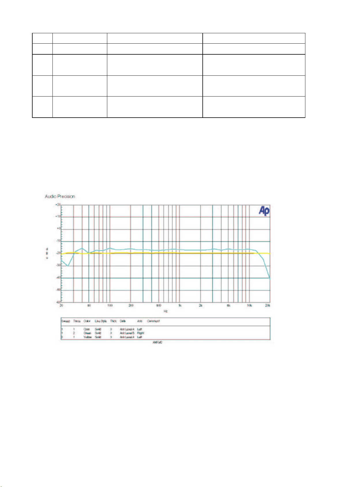
g. rotate the “MIX” knob to minimum, connect the AP output to Right Input, at this moment, only
the “R” has output, rotate the “PRESET” (the larger knob) to “Delay” position, and the
“ VARIATIONS” (the smaller one) to “1” position, also the “MIX” knob to maximum, the sweep
frequency response curve as below:
h. Test for “BYPASS”: rotate the “ MIX” to maximum, connect the footswitch to “BYPASS” jack,
this footswitch can control the DSP effect.
i. When turn off the input signal, the output noise is <-70dbm.
j. Spot-check: to know if there is another noise and the DSP effect is OK.
k. Factory Preset: rotate the “INPUT”, “OUTPUT”, and “MIX” knobs to minimum, the
“ VARIATIONS” (the smaller knob) to “1” position, and the “ PRESETS” (the larger one) to
“ HALL1” position.
Page 13

k
Y
PF03857
S
_
A
_
_
_
r
r
t
A
0
A
A
A
A
A
k
V
k
r
r
7. BOM
- 11 -
0001
0002
0003
0004
0005
0006
0007
0008
0009
0010
0011
0012
0013
0014
0015
0016
0017
0018
0019
0020
0021
0022
0023
0024
0025
0001
0002
0003
0004
0005
0006
0007
0008
0009
0010
0011
0012
0013
0014
0015
0016
Ran
0001
0002
0003
0004
Part No. Description Specification QT
DIGITAL
MULTIEFFECT
MA07059 panel-RS
MB05584 chassis-RS
MC00992 top cover-RS
NI00363 knob-RS
NI02386 konb-RS φ14*13mm 1
NI04996 knob-RS φ11*19(5445C)_V1.0 3
NI04999 knob-RS φ8.5*4(123U)_V1.0 2
NI04998 knob-RS φ8.5*4(298C)_V1.0 1
MG00025 screw-RS M3*6 6
MG00163 screw M3*8 2
NI00002 plastic nut-RS φ7/16"*G20/15*4.8 5
MF00014 washe
NC00131 washe
TG00023 adaptor
HJ00002 dessican
NA00122 PE bag 0.04t*350*230mm 1
NA00146 bubble bag 13*16 1
NI00501 self-adhere foot cushion 12.7*9*3t(SF-004) 4
NE05006 label-RS
NE05004 label
NE02717 label MADE IN CHIN
NF00061 assurance card-RS-C
D00012 twin adhesive-RS 90*120mm_V1.0 1
NA00279 clip-chain bag 0.04t*100*150mm_V1.0 1
HK08950 PC board
CB00072 electrolytic capacitor 1000uF/25V φ10*20mm 1 C10
HI00192 rotary switch 288S0366 2 EN1,EN2
RC00086 potentiometer
RC00087 potentiometer
HC00108 stereo MIC jac
HC00183 DC jack-RS KJ-36-S φ3.5 1 J1
SA00094 rectifier diode 1N4002/100
SD00074 integrated circuit L7805CV(TO220)/(ST) 1 U10
SB00083
SA00053 L.E.D φ3 round(red)long foot 2 LD1,LD2
MI00256 heat-sin
MF00037 washe
MG00166 screw M3*10 1
HC00473 connector-RS
NI02249 plastic washe
HK08951 PC board
CI00007
CI00009
CI00012
CI00018
voltage stabilized
transistor-RS-ACT
SMD ceramic capacitor
0805
SMD ceramic capacitor
0805
SMD ceramic capacitor
0805
SMD ceramic capacitor
0805
aVERB
ALTO_230V_CHIN
αVERB ALTO
αVERB
aVERB
φ21*16mm COOL GRAY
8C/072C_V1.1
φ3*φ6.5*0.5t 2
1*φ11.3*φ15.3 red 5
230V/50Hz_AC9V/300mA_E
T-35_CE
10g 1
LPHAVERB_V1.
LTO 4
LTO_V1.1 1
P-aVERB -N2-DIP
A10KΩ*2 RV16A01-20-20F-
14-301
B1KΩ*2 RV16A01-20-20FB13-301
φ6.3 stereo LJB0661-6 5 PJ1,PJ2,PJ3,PJ4,PJ5
UTC79L05(TO92)/(UTC) 1 U9
25*15*10.6-1PIN SCL-2020 1
φ3.2*φ5.5*1t 1
2.45mm 180° 2*8P B252*8BG1(B)H=5mm
TW-1(TO-220) 1
P-aVERB -N2-SMD
22PF/50V NPO 4 C24,C27,C28,C29
33PF/50V NPO 2 C33,C34
47PF/50V NPO 4 C46,C47,C48,C49
220PF/50V NPO ±5% 2 C9,C25
V1.0
V1.0
V1.0
1
1
1
1
1
1
4
2
1
2 VR1,VR3
1 VR2
2 D2,D3
1 CN2
1
Remark
Page 14

Ran
k
Y
)
0005
0006
0007
0008
0009
0010
0011
0012
0013
0014
0015
0016
0017
0018
0019
0020
0021
0022
0023
0024
0025
0026
0027
0028
0029
Part No. Description Specification QT
C1,C2,C5,C6,C18,
CI00100
CI00112
RD00002 SMD fixed resistor 1/8W 0.0Ω ±5% 0805 1 JP1
RD00006 SMD fixed resistor 1/8W 100Ω ±5% 0805 3 R1,R2,R47
RD00009 SMD fixed resistor 1/8W 220Ω ±5% 0805 2 R41,R42
RD00010 SMD fixed resistor 1/8W 270Ω ±5% 0805 2 R20,R23
RD00014 SMD fixed resistor 1/8W 470Ω ±5% 0805 3 R44,R45,R46
RD00018 SMD fixed resistor 1/8W 1.0KΩ ±5% 0805 3 R4,R12,R37
RD00027 SMD fixed resistor 1/8W 4.7KΩ ±5% 0805 1 R36
RD00031 SMD fixed resistor 1/8W 7.5KΩ ±5% 0805 1 R40
RD00032 SMD fixed resistor 1/8W 10KΩ ±5% 0805 26
RD00044 SMD fixed resistor 1/8W 47KΩ ±5% 0805 1 R35
RD00056 SMD fixed resistor 1/8W 1.0MΩ ±5% 0805 3 R5,R13,R38
RD00057 SMD fixed resistor 1/8W 2.2MΩ ±5% 0805 1 R39
RD00267 SMD fixed resistor 1/8W 820KΩ ±5% 0805 1 R43
RE00011
SE00011 SMD rectifier diode RLS4148 0.5A (LL-34) 5 D1,D4,D5,D6,D7
SF00056 transistor MMBT3904(SOT23)/(PHI) 2 TR1,TR2
SG00001 SMD integrated circuit TL074CDT(SO14)/(ST) 3 U1,U2,U3
SG00306 SMD integrated circuit LM393DR(TI)/(MEXICO) 1 U4
SG00044 SMD integrated circuit BU4066F(SOT73)/(PHI) 1 U7
SG00068 SMD integrated circuit 74HC14DT(SO14)/(PHI) 1 U6
SG00469 SMD integrated circuit- SN74HC109DR(SO16)/(TI) 1 U5
AE00449
HK08952 PC board
CB00189 electrolytic capacitor 1.0uF/50V φ4*5mm 2 C41,C42
0001
CB00190 electrolytic capacitor 4.7uF/25V φ4*7mm 2 C7,C23
0002
CB00192 electrolytic capacitor 10uF/16V φ4*7mm 2 C39,C40
0003
CB00194 electrolytic capacitor 47uF/25V φ5*11mm 7
0004
CB00195 electrolytic capacitor 100uF/16V φ6*7mm 2 C3,C4
0005
CB00251 electrolytic capacitor 220UF/25V φ8*11mm 1 C11
0006
CF00143 metal-film capacitor 0.0015uF/100V 5% CASE01 3 C30,C31,C32
0007
HA01919 jump 5mm 25
0008
HA02441 jump 7.5mm 30
0009
HA01925 jump 10mm 22
0010
HA01935 jump 12.5mm 6 J63,J64,J68,J70,J71,J17
0011
HA01924 jump 9mm 2 J21,J22
0012
SMD ceramic capacitor
0805
SMD ceramic capacitor
0805
SMD resistor networks
1/16W
solder material without
lead
0.1uF/50V X7R ±10% 17
0.01uF/50V X7R ±10% 2 C14,C26
680Ω*4 ±5% 8P
1206(0603x4
9308/Sn Ag Cu 0.3768
P-aVERB -N2-AI
C19,C20,C21,C22,
C35,C36,C37,C38,
C44,C45,C50,C51
R3,R6,R7,R8,R9,R10,
R11,R14,R15,R16,R17,
R18,R19,R21,R22,R24,
R25,R26,R27,R28,R29,
R30,R31,R32,R33,R34
2 AR1,AR2
1
C8,C12,C13,C15,C16,
C17,C43
L1,L2,L3,L4,L5,L6,L7,
L8,L11,L12,L10,L13,
PS1,J28,J29,J37,J40,
J41,J43,J45,J46,J47,
J51,J72,PS1
J50,J49,J48,J44,J42,
J36,J35,J34,J33,J32,
J30,J23,J27,J26,J25,
J24,J18,J16,J15,J12,
J11,J10,J9,J8,J7,J6,
J66,J67,J73,J74
J62,J61,J60,J59,J58,
J57,J56,J55,J54,J53,
J52,J39,J38,J20,J19,
J14,J5,J4,J3,J2,J65,J69
Remark
- 12 -
Page 15

k
Y
A
5
A
t
5
)
Z
b
T
r
r
r
5
r
)
T
)
)
A
0026
O
_
_
T
0027
0028
0029
0030
Ran
0017
0018
0019
0020
0021
0022
0023
0030
0001
0002
0003
0004
0005
0006
0007
Part No. Description Specification QT
HA01930 jump 15mm 1 J31
0013
HB02541 PCB-RS
0014
SG00243 SMD integrated circuit NE555DR(SO8)/(TI) 1 U8
C00179 tin without lead-RS M705E Sn 3Ag-0.5Cu 8.6
NI01776 LED spacer suppor
ME0001
MG00036 screw M3*4 4
MG00284 copper pillar M3*8*0.5PH 4
HK04336 PC board P-313123-DIP(TOPVerb
SC00004 crystal oscillator 16.00MH
HC00512 connector
SG00300 SMD integrated circuit SST39VF010-70n/TOPVer
NE13363 label TOPVerb_V1.0 1
HK03894 PC board-RS-AC
HB00895 PCB 313123/2(1*6) 1
0001
CI00075
0002
RD00061 SMD fixed resisto
0003
RD00068
0004
RD00073 SMD fixed resisto
0005
RD00085
0006
RD00088
0007
RD00101 SMD fixed resisto
0008
RD0012
0009
RE00006
0010
SE00011 SMD rectifier diode RLS4148 0.5A (LL-34) 1 D1
0011
SG00068 SMD integrated circuit 74HC14DT(SO14)/(PHI) 1 IC1
0012
SG00410
0013
SG00166 SMD integrated circuit TY-2 1 IC3
0014
SG00037 SMD integrated circuit LD1117DT33C(TO252)/(ST
0015
HC00611 IC socket (SMD) PLCC32 (AMP S/N:822516
0016
SG00016 SMD integrated circuit UDA1345TS(SSOP28)/(PHI
0017
AE00449
0018
CI00264
0019
C00179 tin without lead-RS M705E Sn 3Ag-0.5Cu 5.058
CB00166 electrolytic capacitor 100uF/16V φ6*5mm 11
RA01234 fixed resistor 1/4W 4.7KΩ 1 R48
NB02141 carton
NB05581 inner case-RS
MG00538 screw M3*10*0.5PH_V1.0 4
NF02910 user manual-RS
NE05847 label-RS-AC
color nut 3m/m 4
SMD ceramic capacitor
0603
SMD fixed resistor
1/10W
SMD fixed resistor
1/10W
SMD fixed resistor
1/10W
SMD fixed resisto
SMD resistor networks
1/16W
SMD integrated circuitRS-AC
solder material without
lead
SMD ceramic capacitorRS 0603
lphaverb_VER07061
LED-3 3mm 2
2.54 180°2*8P(gold-plated)
4/9.5mm
P-313123-SMD(L-8) 1
0.1uF/50V Y5V +80,-20% 13
10Ω ±5% 0603 1 R22
100Ω ±5% 0603 8
220Ω ±5% 0603 1 R3
1.5KΩ ±5% 0603 10
2.2KΩ ±5% 0603 8
10KΩ ±5% 0603 3 R32,R31,R1
1.0MΩ ±5% 0603 1 R2
100KΩ*4 ±5% 8P
1206(0603x4
IC41LV1625635KG(SOJ40)/(ICSI)
9308/Sn Ag Cu 0.3864
15PF/50V NPO ±5
a VERB;a COMP;a
MICTUBE ALT
αVERB ALTO
αVERB ALTO
aVERB II_V1.0 1
V1.0
V1.0
Remark
1
1
1 XT
1 CN2
1 IC4
C17,C15,C18,C6,C10,
C22,C20,C13,C14,C1,
C3,C4,C11
R12,R14,R7,R8,R34,
R17,R13,R33
R16,R15,R21,R20,R4,
R19,R10,R18,R9,R5
R28,R27,R23,R24,
R29,R30,R25,R26
2 AR1,AR2
1 IC6
1 IC2
1 IC4
1 IC5
2 C8,C9
C19,C12,C5,C2,
C24,C16,C21,C25,
C26,C28,C7
1
1
1
- 13 -
Page 16

8. EXPLODED VIEWS & MECHANICAL PARTS LIST
- 14 -
Page 17

No. Part No. Description Specification QTY
(
)
p
φ
_
p
φ
p
φ
φ
pp
p
φ3*φ
(
)
p
_
φ
φ
p
φ
y)_
- 15 -
MECHANICAL PARTS LIST
1 NI00501 self-adhesive foot cushion-RS 12.7*9*3t
2 NI00363
3 NI00002
4 NI02386
5 NC00131 T-washer-RS-ACT 1*
6 MG0028 co
7 MF00014 washer-RS-ACT-zinc
lastic knob-RS-C
lastic nut-RS
lastic knob-RS-C
21*16mm COOL GRAY 8C 072C
7/16"*G20/15*4.8 5
14*13mm (cool gray 8C 072C 1
11.3*φ15.3 red 5
er pillar-RS M3*8*0.5PH 14 4
lated
SF-004
6.5*0.5t 2
4
1
8 MG0003 screw-RS M3*4 4
9 MG0016 nickle screw-RS M3*8 2
10 HK04336 K-PCB 313123-DIP
11 MC0099 ZB-to
12 NI04999 knob-RS-CT-ABS
13 NI04998 knob-RS-CT-ABS
14 NI04996
15 MB05584 ZC-chassis-RS-
16 MA07059 ZC-front panel-RS-5063 blue
17 HK08950 K-PCB
cover-RS-5252
lastic knob-RS-CT-
aVERB
8.5*4(123U yellow)_V1.0 2
8.5*4(298C blue)_V1.0 1
11*19(5445C gra
αVERB _V1.0
αVERB ALTO_V1.0
aVERB -N2-DIP
TOPVerb
V1.0
1
1
V1.0 3
1
1
1
18 MG0002 screw-RS M3*6 6
19 ME00015 color nut-RS 3mm 4
 Loading...