

Page 1

SDI II IP Core User Guide
Last updated for Altera Complete Design Suite: 15.0
Subscribe
Send Feedback
UG-01125
2015.05.04
101 Innovation Drive
San Jose, CA 95134
www.altera.com
Page 2

TOC-2
Contents
SDI II IP Core Quick Reference..........................................................................1-1
SDI II IP Core Overview......................................................................................2-1
SDI II IP Core Getting Started............................................................................3-1
General Description.....................................................................................................................................2-1
SMPTE372 Dual Link Support.......................................................................................................2-2
SMPTE RP168 Switching Support.................................................................................................2-6
SD 20-Bit Interface for Dual/Triple Standard..............................................................................2-6
Dynamic TX Clock Switching........................................................................................................2-7
Resource Utilization.................................................................................................................................... 2-9
Installation and Licensing...........................................................................................................................3-1
Design Walkthrough................................................................................................................................... 3-1
Creating a New Quartus II Project................................................................................................3-2
Launching IP Catalog......................................................................................................................3-2
Parameterizing the IP Core............................................................................................................ 3-3
Generating a Design Example and Simulation Testbench.........................................................3-3
Simulating the SDI II IP Core Design...........................................................................................3-3
Compiling the SDI II IP Core Design.......................................................................................................3-4
Programming an FPGA Device................................................................................................................. 3-5
Design Reference..........................................................................................................................................3-5
SDI II IP Core Parameters..............................................................................................................3-6
SDI II IP Core Component Files....................................................................................................3-9
Design Examples..............................................................................................................................3-9
Video Pattern Generator Signals................................................................................................. 3-22
Transceiver Reconfiguration Controller Signals.......................................................................3-23
Reconfiguration Management Parameters.................................................................................3-26
Reconfiguration Router Signals...................................................................................................3-27
SDI II IP Core Functional Description...............................................................4-1
Altera Corporation
Protocol......................................................................................................................................................... 4-2
Transmitter.......................................................................................................................................4-2
Receiver............................................................................................................................................. 4-6
Transceiver..................................................................................................................................................4-12
Submodules.................................................................................................................................................4-14
Insert Line.......................................................................................................................................4-14
Insert/Check CRC..........................................................................................................................4-15
Insert Payload ID........................................................................................................................... 4-15
Match TRS...................................................................................................................................... 4-17
Scrambler........................................................................................................................................ 4-17
Page 3

TOC-3
TX Sample.......................................................................................................................................4-18
Clock Enable Generator................................................................................................................4-18
RX Sample.......................................................................................................................................4-19
Detect Video Standard..................................................................................................................4-21
Detect 1 and 1/1.001 Rates............................................................................................................4-21
Transceiver Controller..................................................................................................................4-21
Descrambler....................................................................................................................................4-22
TRS Aligner.....................................................................................................................................4-23
3Gb Demux.....................................................................................................................................4-24
Extract Line.....................................................................................................................................4-24
Extract Payload ID.........................................................................................................................4-24
Detect Format.................................................................................................................................4-24
Sync Streams...................................................................................................................................4-25
Convert SD Bits..............................................................................................................................4-26
Insert Sync Bits...............................................................................................................................4-26
Clocking Scheme........................................................................................................................................4-27
SDI II IP Core Signals................................................................................................................................4-27
Additional Information......................................................................................A-1
Document Revision History......................................................................................................................A-1
Altera Corporation
Page 4
2015.05.04
www.altera.com
101 Innovation Drive, San Jose, CA 95134
SDI II IP Core Quick Reference
1
UG-01125
Subscribe
Send Feedback
The Altera® Serial Digital Interface (SDI) II MegaCore® function is the next generation SDI intellectual
property (IP).
The SDI II IP core is part of the MegaCore IP Library, which is distributed with the Quartus® II software
and downloadable from the Altera website at www.altera.com.
Note:
For system requirements and installation instructions, refer to Altera Software Installation &
Licensing.
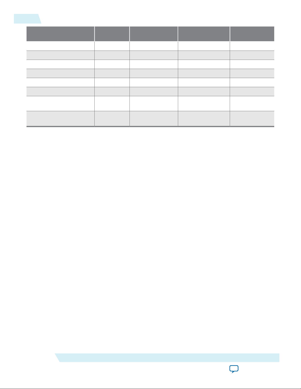
Table 1-1: Brief Information About the SDI II IP Core
Item Description
Version 15.0
Release Date May 2015
Release
Information
Ordering Code IP-SDI-II
Product ID(s) 0111
Vendor ID 6AF7
SDI Data Rate
Support
• 270-Mbps SD-SDI, as defined by SMPTE259M specification
• 1.485-Gbps or 1.4835-Gbps HD-SDI, as defined by
SMPTE292M specification
• 2.97-Gbps or 2.967-Gbps 3G-SDI, as defined by SMPTE424M
specification
• 5.94-Gbps or 5.934-Gbps 6G-SDI, as defined by SMPTEST2081
IP Core
Information
specification
• 11.88-Gbps or 11.868-Gbps 12G-SDI, as defined by
SMPTEST2082 specification
• Dual link HD-SDI, as defined by SMPTE372M specification
• Dual standard support for SD-SDI and HD-SDI
• Triple standard support for SD-SDI, HD-SDI, and 3G-SDI
• Multi standard support for SD-SDI, HD-SDI, 3G-SDI, 6G-SDI,
and 12G-SDI
©
2015 Altera Corporation. All rights reserved. ALTERA, ARRIA, CYCLONE, ENPIRION, MAX, MEGACORE, NIOS, QUARTUS and STRATIX words and logos are
trademarks of Altera Corporation and registered in the U.S. Patent and Trademark Office and in other countries. All other words and logos identified as
trademarks or service marks are the property of their respective holders as described at www.altera.com/common/legal.html. Altera warrants performance
of its semiconductor products to current specifications in accordance with Altera's standard warranty, but reserves the right to make changes to any
products and services at any time without notice. Altera assumes no responsibility or liability arising out of the application or use of any information,
product, or service described herein except as expressly agreed to in writing by Altera. Altera customers are advised to obtain the latest version of device
specifications before relying on any published information and before placing orders for products or services.
ISO
9001:2008
Registered
Page 5

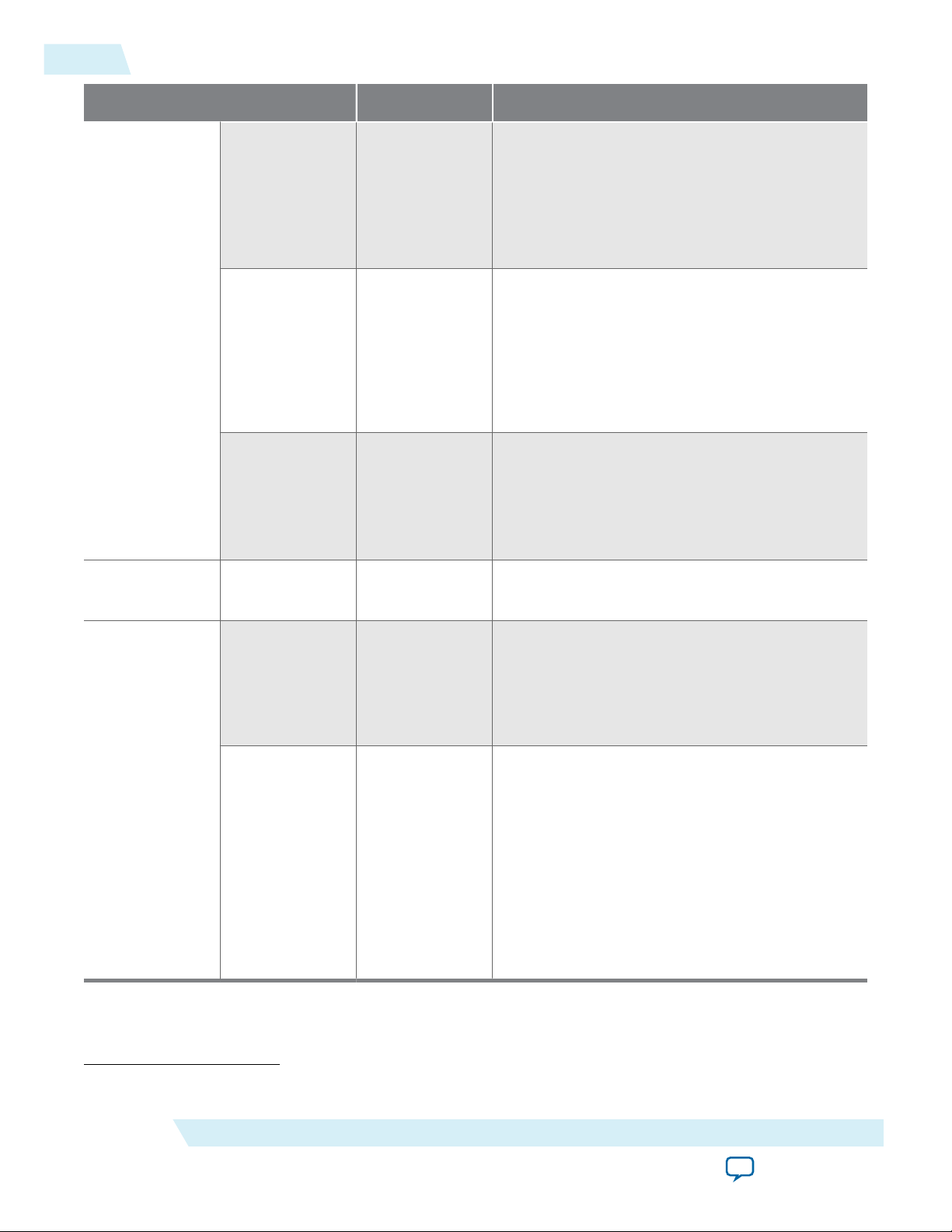
1-2
SDI II IP Core Quick Reference
Item Description
Features • 20-bit interface support for SD-SDI
UG-01125
2015.05.04
• Multiple SDI standards and video formats
• Payload identification packet insertion and extraction
• Clock enable generator
• Video rate detection
• Cyclical redundancy check (CRC) encoding and decoding
(except SD)
• Line number (LN) insertion and extraction (except SD)
• Word scrambling and descrambling
• Word alignment
• Framing and extraction of video timing signals
• Dual link data stream synchronization (except SD)
• Transceiver dynamic reconfiguration
• RP168 support for synchronous video switching
• Dynamic TX clock switching
• OpenCore Plus evaluation
• SMPTE425M level A support (direct source image formatting)
• SMPTE425M level B support (dual link mapping)
Application • Digital video equipment
• Mixing and recording equipment
Device Family
Support
Arria® 10 (preliminary), Arria V GX, Arria V GZ, Cyclone® V,
and Stratix® V FPGA device families.
Refer to the device support table and What’s New in Altera page of
the Altera website for detailed information.
Design Tools • IP Catalog in the Quartus II software for design creation and
compilation
• ModelSim®-Altera, Riviera-Pro, and VCS/VCS MX software
for design simulation or synthesis
Related Information
• Altera Software Installation and Licensing
• What's New in Altera IP
Altera Corporation
SDI II IP Core Quick Reference
Send Feedback
Page 6

2015.05.04
www.altera.com
101 Innovation Drive, San Jose, CA 95134
SDI II IP Core Overview
2
UG-01125
Subscribe
Send Feedback
The SDI II IP core implements a transmitter, receiver, or full-duplex SDI at standard definition (SD), high
definition (HD), or 3 gigabits per second (3G) to 12G rate as defined by the Society of Motion Picture and
Television Engineers (SMPTE). The SDI II IP core supports dual standard (SD-SDI and HD-SDI), triple
standard (SD-SDI, HD-SDI, and 3G-SDI) and multi standard (SD-SDI, HD-SDI, 3G-SDI, 6G-SDI, and
12G-SDI). These modes provide automatic receiver rate detection and transceiver dynamic reconfigura‐
tion.
The SDI II IP core highlights the following new features:
• Supports 28 nm devices and beyond.
• Arria V GX and Stratix V from Quartus II version 12.1 onwards
• Arria V GZ and Cyclone V from Quartus II version 13.0 onwards
• Arria 10 from Quartus II version 14.0A10 onwards
• Improved integration with Altera tools (hw.tcl).
• IEEE encryption for functional simulation.
• Dynamic generation of user simulation testbench that matches the IP configuration.
• Dynamic generation of design example that serves as common entity for simulation and hardware
verification.
General Description
The SMPTE defines a SDI standard that is widely used as an interconnect between equipment in video
production facilities. The SDI II IP core can handle the following SDI data rates:
• 270 megabits per second (Mbps) SD-SDI, as defined by SMPTE259M-1997 10-Bit 4:2:2 Component
Serial Digital Interface
• 1.485 gigabits per second (Gbps) or 1.4835-Gbps HD-SDI, as defined by SMPTE292M-1998 Bit-Serial
Digital Interface for High Definition Television Systems
• 2.97-Gbps or 2.967-Gbps 3G SDI, as defined by SMPTE424M
• 5.94-Gbps or 5.934-Gbps 6G-SDI, as defined by SMPTEST2081
• 11.88-Gbps or 11.868-Gbps 12G-SDI, as defined by SMPTEST2082
• Dual link HD-SDI, as defined by SMPTE372M-Dual Link 1.5Gb/s Digital Interface for 1920×1080 and
2048×1080 Picture Formats
• Dual standard support for SD-SDI and HD-SDI
©
2015 Altera Corporation. All rights reserved. ALTERA, ARRIA, CYCLONE, ENPIRION, MAX, MEGACORE, NIOS, QUARTUS and STRATIX words and logos are
trademarks of Altera Corporation and registered in the U.S. Patent and Trademark Office and in other countries. All other words and logos identified as
trademarks or service marks are the property of their respective holders as described at www.altera.com/common/legal.html. Altera warrants performance
of its semiconductor products to current specifications in accordance with Altera's standard warranty, but reserves the right to make changes to any
products and services at any time without notice. Altera assumes no responsibility or liability arising out of the application or use of any information,
product, or service described herein except as expressly agreed to in writing by Altera. Altera customers are advised to obtain the latest version of device
specifications before relying on any published information and before placing orders for products or services.
ISO
9001:2008
Registered
Page 7
2-2
SMPTE372 Dual Link Support
• Triple standard support for SD-SDI, HD-SDI, and 3G-SDI
• Multi standard support for SD-SDI, HD-SDI, 3G-SDI, 6G-SDI, and 12G-SDI
• SMPTE425M level A support (direct source image formatting)
• SMPTE425M level B support (dual link mapping)
• SMPTE RP168 switching support
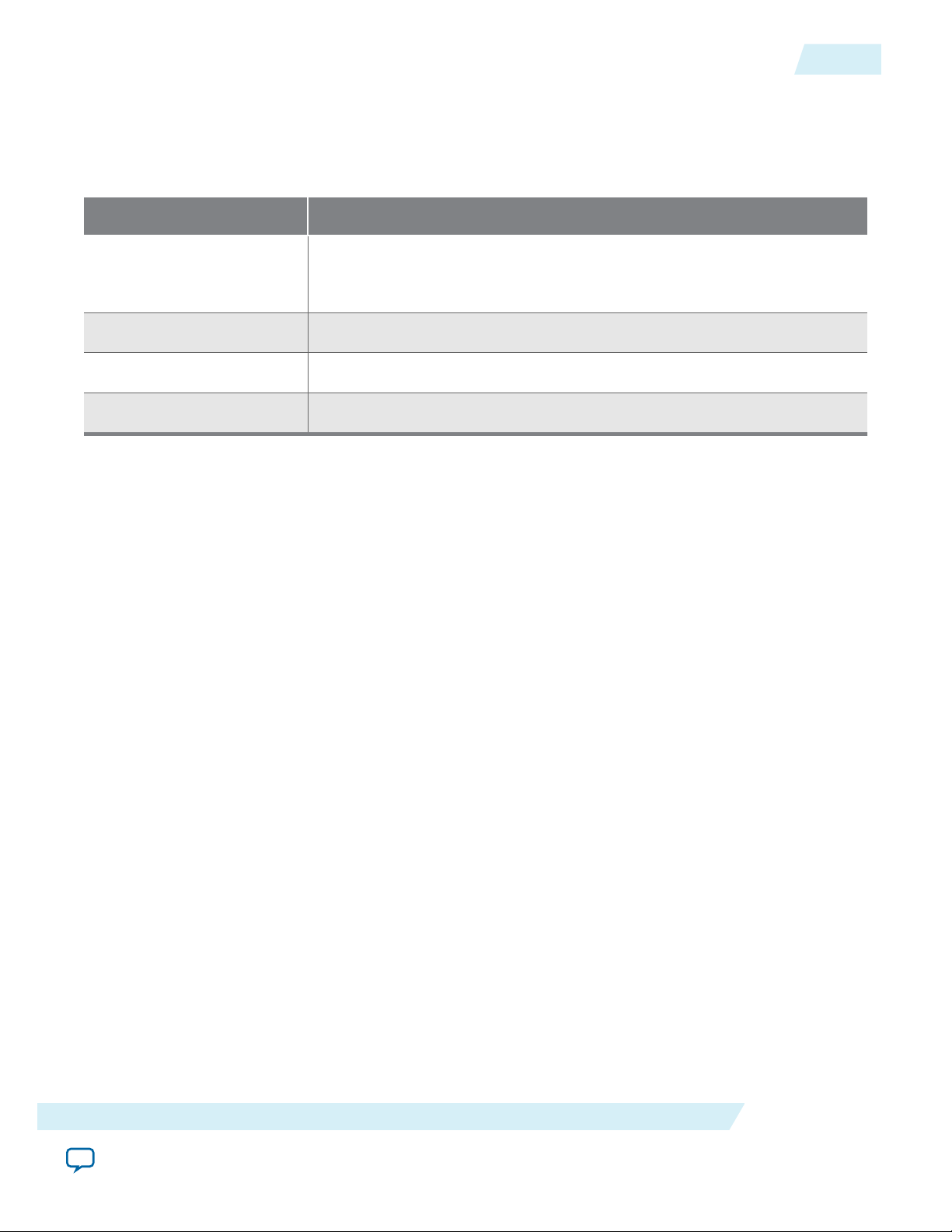
Table 2-1: SDI Standard Support
Table below lists the SDI standard support for various FPGA devices.
SDI Standard
Single Standard Multiple Standards
Device Family
SD-SDI HD-SDI 3G-SDI Dual Link
HD-SDI
Dual
Standard
(up to HD)
Triple
Standard
(up to 3G)
UG-01125
2015.05.04
Multi Standard
(up to 12G)
Arria V
Yes Yes Yes Yes Yes Yes No
GX
Arria V
Yes Yes Yes Yes Yes Yes No
GZ
Stratix V Yes Yes Yes Yes Yes Yes No
Cyclone V Yes Yes Yes Yes Yes Yes No
Arria 10 No Yes Yes Yes No Yes Yes
SMPTE372 Dual Link Support
Recording studios support HD 1080p format by using a dual-link connection (SMPTE372) from cameras
to the mixing and recording equipment. The SMPTE 372 specification defines a way of interconnecting
digital video equipment with a dual link HD-SDI, based upon the SMPTE292 specification data structure.
The total data rate of the dual link connection is 2.97 Gbps or 2.97/1.001 Gbps.
HD-SDI Dual Link to 3G-SDI (Level B) Conversion
To interface between a HD-SDI dual link receiver and 3G-SDI single link transmitter equipment, perform
a HD-SDI dual link to 3G-SDI (level B) conversion. Level B is defined as 2× SMPTE292 HD-SDI
mapping, including SMPTE372 dual link mapping.
This conversion takes either two 1.485 Gbps dual link signals or two separate co-timed HD signals and
combines them into a single 3G-SDI stream.
Altera Corporation
SDI II IP Core Overview
Send Feedback
Page 8
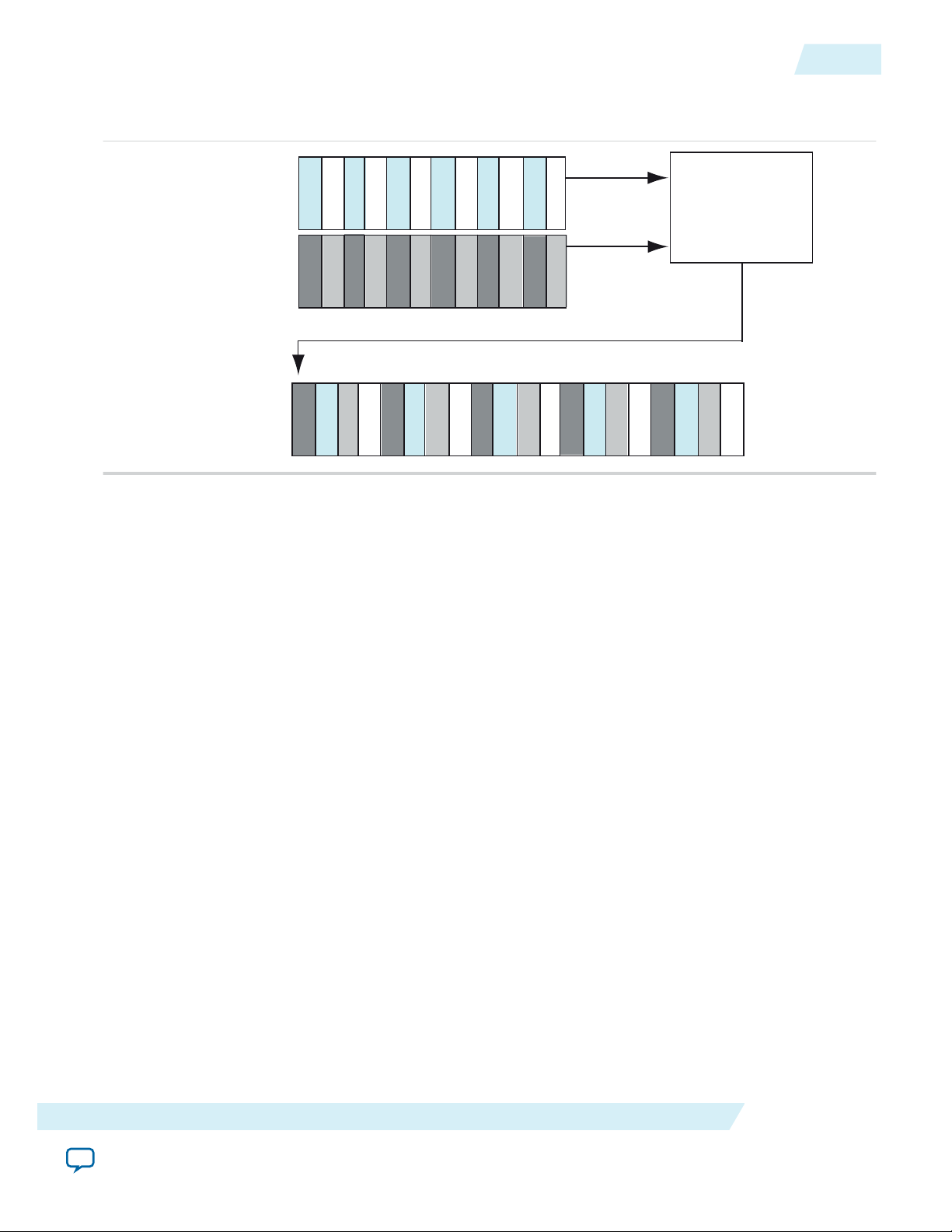
3FFh(C1)
3FFh(Y1)
000h(C1)
000h(Y1)
XYZ(C1)
XYZ(Y1)
LN0(C1)
LN0(Y1)
LN1(C1)
LN1(Y1)
3FFh(C2)
3FFh(Y2)
000h(C2)
000h(Y2)
XYZ(C2)
XYZ(Y2)
LN0(C2)
LN0(Y2)
LN1(C2)
LN1(Y2)
000h(C1)
000h(Y1)
000h(C2)
000h(Y2)
Multiplexing
Data Stream 1
Data Stream 2
3G-SDI Level B
Interleaved Stream
3FFh(C2)
3FFh(C1)
3FFh(Y2)
3FFh(Y1)
000h(C2)
000h(C1)
000h(Y2)
000h(Y1)
XYZ(C2)
XYZ(C1)
XYZ(Y2)
XYZ(Y1)
LN0(C2)
LN0(C1)
LN0(Y2)
LN0(Y1)
LN1(C2)
LN1(C1)
LN1(Y2)
LN1(Y1)
UG-01125
2015.05.04
HD-SDI Dual Link to 3G-SDI (Level B) Conversion
Figure 2-1: Example of HD-SDI Dual Link to 3G-SDI (Level B) Conversion
The figure shows the conversion of two HD-SDI data streams to 3G-SDI (level B) data streams.
2-3
SDI II IP Core Overview
Send Feedback
Altera Corporation
Page 9
Transceiver
HD Link A
Protocol FIFO
rxdataA rxdataA rdreq
Transceiver
HD Link B
Protocol FIFO
rxdataB rxdataB
rdreq
Divide
Clock
rx_clkin_smpte372
(148.5 MHz or 148.35 MHz)
rx_dataout[19:0]
rdclk_3gb_div2 =
1H1L1H1L
xcvr_refclk (74.25 MHz or 74.175 MHz)
rx_clkout
(74.25 MHz or 74.175 MHz)
rx_clkout_b
(74.25 MHz or 74.175 MHz)
Sync Stream
HD Dual-Link Receiver
Y1 Y1 Y1 Y1
C1 C1 C1 C1
Y2 Y2 Y2 Y2
C2 C2 C2 C2
rx_clkout
rxdataA[19:10]
rxdataA[9:0]
rx_clkout_b
rxdataB[19:10]
rxdataB[9:0]
rx_clkin_smpte372
rdclk_3gb_div2
rx_dataout[19:10]
rx_dataout[9:0]
C1 C1 C1 C1Y1 Y1 Y1 Y1
C2 C2 C2 C2Y2 Y2 Y2 Y2
2-4
3G-SDI (Level B) to HD-SDI Dual Link Conversion
Figure 2-2: Implementation of HD-SDI Dual Link to 3G-SDI (Level B) Conversion
The figure shows a block diagram of HD-SDI dual link to 3G-SDI (level B) conversion.
UG-01125
2015.05.04
Altera Corporation
3G-SDI (Level B) to HD-SDI Dual Link Conversion
To interface between 3-Gbps single link receiver and HD-SDI dual link transmitter equipment, perform a
3G-SDI (level B) to HD-SDI dual link conversion. This conversion takes a single 3G-SDI signal and
separates the signal into two 1.485 Gbps signals, which can either be a dual link 1080p signal or two
separate co-timed HD data streams.
SDI II IP Core Overview
Send Feedback
Page 10
3FFh(C2)
Demux
3FFh(C1)
3FFh(Y2)
3FFh(Y1)
000h(C2)
000h(C1)
000h(Y2)
000h(Y1)
XYZ(C2)
XYZ(C1)
XYZ(Y2)
XYZ(Y1)
LN0(C2)
LN0(C1)
LN0(Y2)
LN0(Y1)
LN1(C2)
LN1(C1)
LN1(Y2)
LN1(Y1)
3FFh(C1)
3FFh(Y1)
000h(C1)
000h(Y1)
XYZ(C1)
XYZ(Y1)
LN0(C1)
LN0(Y1)
LN1(C1)
LN1(Y1)
3FFh(C2)
3FFh(Y2)
000h(C2)
000h(Y2)
XYZ(C2)
XYZ(Y2)
LN0(C2)
LN0(Y2)
LN1(C2)
LN1(Y2)
000h(C1)
000h(Y1)
000h(C2)
000h(Y2)
3G-SDI Level B Interleaved Stream
Data Stream 1
HD-SDI Link A (10-bit)
HD-SDI Link B (10-bit)
Data Stream 2
Transceiver
3-GB Signal
Protocol
3-GB
Demux
rxdata
rx_clkin_smpte372
(74.25 MHz or 74.175 MHz)
rx_dataout[19:0]
rdclk_3gb_div2 =
1H1L1H1L
xcvr_refclk (148.5 MHz or 148.35 MHz)
rx_clkout
(148.5 MHz or 148.35 MHz)
FIFO
rx_dataout_b[19:0]
rx_dataout[19:0]
rx_dataout_b[19:0]
wrreq
rxdata[19:0]
rx_trs
3-GB Receiver
rx_clkout
rx_trs
rxdata[19:10]
rxdata[9:0]
C1 C1 C1 C1Y1 Y1 Y1 Y1
C2 C2 C2 C2Y2 Y2 Y2 Y2
Y1 Y1 Y1 Y1
C1 C1 C1 C1
Y2 Y2 Y2 Y2
C2 C2 C2 C2
rx_clkin_smpte372
rx_dataout[19:10]
rx_dataout[9:0]
rx_clkdiv2
rx_dataout_b[19:10]
rx_dataout_b[9:0]
rx_clkout
rx_trs
UG-01125
2015.05.04
3G-SDI (Level B) to HD-SDI Dual Link Conversion
Figure 2-3: Example of 3G-SDI (Level B) to HD-SDI Dual Link Conversion
The figure shows the conversion of 3G-SDI (level B) data to two HD-SDI data streams.
Figure 2-4: Implementation of 3G-SDI (Level B) to HD-SDI Dual Link Conversion
2-5
The figure shows a block diagram of 3G-SDI (level B) to HD-SDI dual link conversion.
SDI II IP Core Overview
Send Feedback
Altera Corporation
Page 11
rx_clkout(148.5 MHz)
rx_dataout[19:10]
rx_dataout[9:0]
rx_dataout_valid
Don’t Care
Cb Y Cr Y Cb
rx_clkout(148.5 MHz)
rx_dataout[19:10]
rx_dataout[9:0]
rx_dataout_valid
Cb
Y
Cr
Y Y
Cb
2-6
SMPTE RP168 Switching Support
SMPTE RP168 Switching Support
The SMPTE RP168 standard defines the requirements for synchronous switching between two video
sources to take place with minimal interference to the receiver. The RP168 standard has restrictions for
which lines the source switching can occur.
The SDI II IP core has flexibility and does not restrict you to switch at only a particular line defined in the
RP168 standard. You can perform switching at any time between different video sources as long as the
source has similar standard and format. After switching, all the status output signals, including the
rx_trs_locked, rx_frame_locked, and rx_align_locked signals, remain unchanged. You should
should not see any interrupts at downstream.
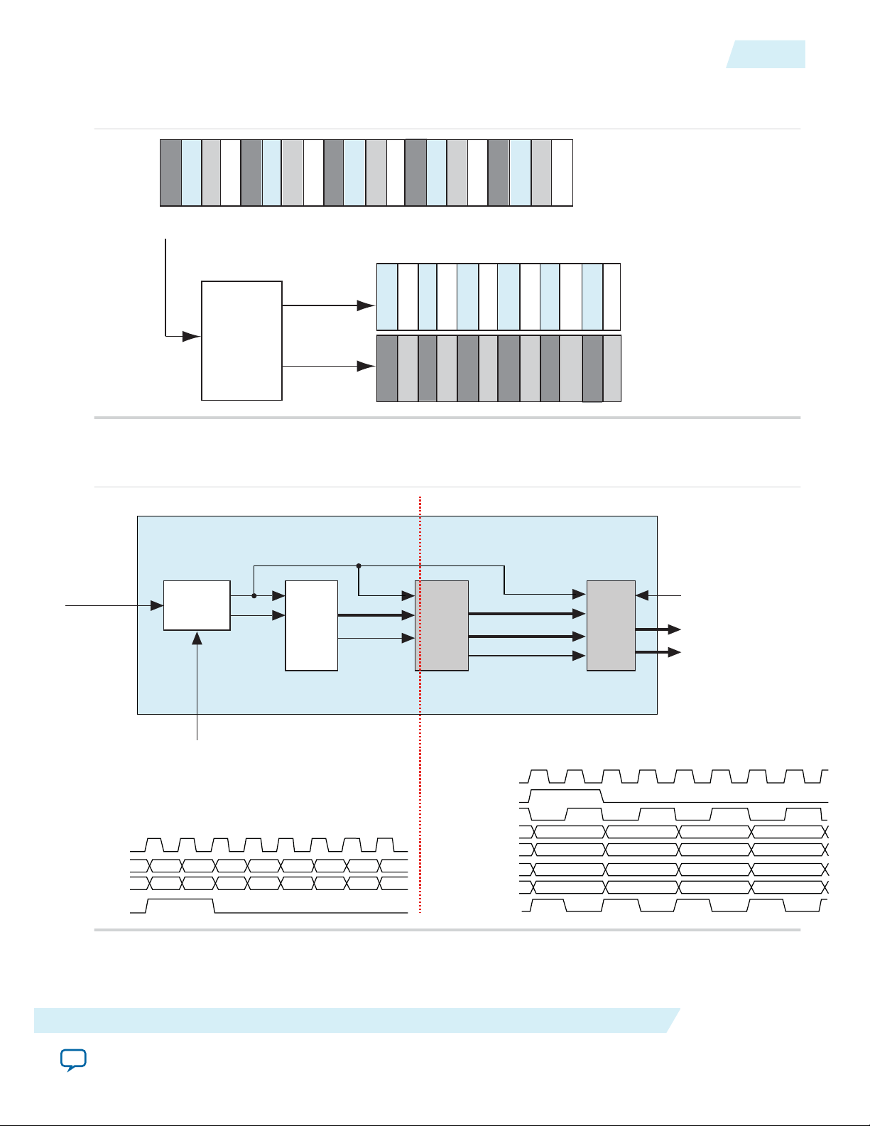
SD 20-Bit Interface for Dual/Triple Standard
For a common SD interface, the serial data format is 10 bits wide, whereas for HD or 3G, the data format
is 20 bits wide, divided into two parallel 10-bit datastreams (known as Y and C).
To make the interface bit width common for all standards in the dual standard or triple standard SDI
mode:
• The receiver can extract the data and align them in 20-bit width
• The transmitter can accept SD data in 20-bit width and retransmit them successfully
UG-01125
2015.05.04
The timing diagrams below show a comparison of data arrangement between 10-bit and 20-bit interface.
Figure 2-5: SD 10-Bit Interface
• The upper 10 bits of rx_dataout are insignificant data.
• The lower 10 bits of rx_dataout are Luma (Y) and chroma (Cb, Cr) channels (interleaved).
• The 1H 4L 1H 5L cadence of rx_dataout_valid repeats indefinitely (ideal).
Figure 2-6: SD 20-Bit Interface
Altera Corporation
• The upper 10 bits of rx_dataout are Luma (Y) channel and the lower 10 bits are Chroma (Cb, Cr)
channel.
• The 1H 10L cadence of rx_dataout_valid repeats indefinitely (ideal).
SDI II IP Core Overview
Send Feedback
Page 12

UG-01125
2015.05.04
Dynamic TX Clock Switching
The dynamic TX clock switching feature allows you to dynamically switch between NTSC and PAL
transceiver data rates for all video standards except SD-SDI. The dynamic TX clock switching enables an
SDI video equipment to operate on NTSC or PAL.
You can choose to switch the TX clocks through one of these two methods:
• Instantiate an alternate TX PLL and supply two different clocks to the two PLLs. Switch between the
primary PLL and the alternate PLL for transmission.
• Use the primary PLL with two reference input clocks. The PLL switches between these two clocks for
transmission.
To implement this feature, you are required to provide two reference clocks (xcvr_refclk and
xcvr_refclk_alt) to the SDI II IP core. The frequency of the reference clocks must be assigned to 148.5
MHz and 148.35 MHz in any assignment order.
The TX PLL select signal (ch1_{tx/du}_tx_pll_sel) is an input control signal that you provide to the
core and the transceiver reconfiguration controller to select the desired clock input for the hard
transceiver.
• Set ch1_{tx/du}_tx_pll_sel to 0 to select xcvr_refclk
• Set ch1_{tx/du}_tx_pll_sel to 1 to select xcvr_refclk_alt
Dynamic TX Clock Switching
2-7
To dynamically switch between the two reference clocks, you need to implement a simple handshaking
mechanism. The handshake is initiated when the reconfiguration request signal (ch1_{tx/
du}_tx_start_reconfig) is asserted high. This signal must remain asserted until the reconfiguration
process completes. The reconfiguration process completes when the reconfiguration done signal
(ch1_{tx/du}_tx_reconfig_done) is asserted high. The TX PLL select signal (ch1_{tx/
du}_tx_pll_sel) needs to be stable throughout the reconfiguration process.
To complete the handshaking process, you must deassert the reconfiguration request signal (ch1_{tx/
du}_tx_start_reconfig) upon assertion of the reconfiguration done signal (ch1_{tx/
du}_tx_reconfig_done). The dynamic TX clock switching only takes effect after the tx_rst is asserted
high and deasserted low accordingly.
SDI II IP Core Overview
Send Feedback
Altera Corporation
Page 13
TX Protocol
TX PHY
Management
PHY Adapter
Transceiver
PHY Reset
Controller
Transceiver
Reconfiguration
Controller
Reconfiguration
Management
Reconfiguration
Router
TX Transceiver
Channel
TX PLL0 TX PLL1
Parallel Video In
(tx_datain and
tx_datain_b for
HD-SDI Dual Link)
Primary Reference Clock (xcvr_refclk)
Alternative Reference Clock (xcvr_refclk_alt)
Reset
(tx_rst)
Tx PLL Switching
Handshaking
Signals
Reconfiguration Acknowledge
(ch1_{tx/du}_tx_reconfig_done)
Reconfiguration Request
(ch1_{tx/du}_tx_start_reconfig)
TX PLL Select (ch1_{tx/du}_tx_pll_sel)
Avalon-MM
Control Interface
TX Clock Out (tx_clkout)
(148.5 or 148.35 MHz)
SDI Out
(sdi_tx and sdi_tx_b for
HD-SDI Dual Link)
Altera Transceiver
Analog Reset
Digital Reset
PLL Powerdown
PLL Locked
Cal Busy
TX PLL Select
SDI TX (All Video Standard Modes except SD-SDI)
Altera PHY
IP Core
Data
Control/Status
Clock
Reset
Legend
148.5 MHz
148.35 MHz
148.5 MHz
Case 1 Case 2 Case 3
148.35 MHz 148.5 MHz 148.35 MHz
xcvr_refclk
xcvr_refclk_alt
tx_rst
ch1_{tx/du}_tx_pll_sel
ch1_{tx/du}_tx_start_reconfig
ch1_{tx/du}_tx_reconfig_done
tx_clkout
2-8
Dynamic TX Clock Switching
Figure 2-7: Hardware Implementation of the Dynamic TX Clock Switching Feature
The figure shows the TX clock switching feature with two TX PLLs.
UG-01125
2015.05.04
Figure 2-8: Dynamic TX Clock Switching Timing Diagram
The table below describes the behavior of the dynamic switching feature when you initiate a handshaking
process (with reference to the timing diagram).
Altera Corporation
SDI II IP Core Overview
Send Feedback
Page 14
UG-01125
2015.05.04
Table 2-2: Dynamic Switching Behavior During a Handshaking Process
Case Description
1 The handshaking process attempts to switch to select xcvr_refclk_alt. tx_clkout success‐
fully locks to xcvr_refclk_alt (148.35 MHz).
2 The handshaking process attempts to switch to select xcvr_refclk. tx_clkout successfully
locks to xcvr_refclk (148.5 MHz).
3 The handshaking process attempts to switch to select xcvr_refclk_alt. The switching fails
because ch1_{tx/du}_tx_pll_sel changes from 1 to 0 prior to the assertion of ch1_{tx/
du}_tx_start_reconfig. Therefore tx_clkout is still locked to xcvr_refclk (148.5MHz).
Resource Utilization
The tables below list the typical resource utilization for the SDI II IP core with the Quartus II software,
version 15.0.
Note:
The resource utilization data was obtained by using the most common configurations for each
video standard and from one specific family device.
Resource Utilization
2-9
Table 2-3: Resource Utilization for Each Video Standard (Arria V, Cyclone V, and Stratix V Devices)
Standard ALM Needed Primary Logic
Registers
Secondary Logic
Registers
Block Memory Bits
SD-SDI TX 95 126 10 0
SD-SDI RX 528 641 48 60
HD-SDI TX 141 159 10 0
HD-SDI RX 557 821 60 0
HD Dual Link TX 447 478 43 0
HD Dual Link RX 1,305 1,897 155 4,608
3G-SDI TX 444 414 12 0
3G-SDI RX 826 1307 125 0
Dual Rate TX 242 237 4 0
Dual Rate RX 924 1,209 84 0
Triple Rate TX 496 528 8 0
Triple Rate RX 1,064 1,583 98 0
Table 2-4: Resource Utilization for Each Video Standard (Arria 10 Devices)
Standard ALM Needed Primary Logic
HD-SDI TX 106 124 23 0
HD-SDI RX 523 765 66 0
SDI II IP Core Overview
Send Feedback
Registers
Secondary Logic
Registers
Block Memory Bits
Altera Corporation
Page 15
2-10
Resource Utilization
UG-01125
2015.05.04
Standard ALM Needed Primary Logic
Registers
Secondary Logic
Registers
Block Memory Bits
HD Dual Link TX 367 410 60 0
HD Dual Link RX 1,239 1,780 177 4,608
3G-SDI TX 407 380 13 0
3G-SDI RX 808 1,261 93 0
Triple Rate TX 475 492 9 0
Triple Rate RX 1024 1,535 86 0
Multi Rate (Up to 12G-
1,807 1,742 24 0
SDI) TX
Multi Rate (Up to 12G-
3,581 4,734 270 0
SDI) RX
Altera Corporation
SDI II IP Core Overview
Send Feedback
Page 16

2015.05.04
www.altera.com
101 Innovation Drive, San Jose, CA 95134
SDI II IP Core Getting Started
3
UG-01125
Subscribe
Installation and Licensing
To evaluate the SDI II IP core using the OpenCore Plus feature, follow these steps in your design flow:
1. Install the SDI II IP core.
2. Create a custom variation of the SDI II IP core.
3. Implement the rest of your design using the design entry method of your choice.
4. Use the IP functional simulation model to verify the operation of your design.
5. Compile your design in the Quartus II software. You can also generate an OpenCore Plus time-limited
programming file, which you can use to verify the operation of your design in hardware.
For more information on IP functional simulation models, refer to the Simulating Altera Designs
Note:
chapter in volume 3 of the Quartus II Handbook.
The default installation directory for the SDI II IP core on Windows is c:\altera\<version>; on Linux, it is /
opt/ altera<version>.
You can obtain a license for the IP core only when you are completely satisfied with its functionality and
performance, and want to take your design to production. After you purchase a license for the SDI II IP
core, follow these steps:
1. Set up licensing.
2. Generate a programming file for the Altera device or devices on your board.
3. Program the Altera device or devices with the completed design.
Send Feedback
Related Information
Simulating Altera Designs
Design Walkthrough
This walkthrough explains how to create an SDI II IP core design using the Quartus II software and IP
Catalog. After you generate a custom variation of the SDI II IP core, you can incorporate it into your
overall project.
©
2015 Altera Corporation. All rights reserved. ALTERA, ARRIA, CYCLONE, ENPIRION, MAX, MEGACORE, NIOS, QUARTUS and STRATIX words and logos are
trademarks of Altera Corporation and registered in the U.S. Patent and Trademark Office and in other countries. All other words and logos identified as
trademarks or service marks are the property of their respective holders as described at www.altera.com/common/legal.html. Altera warrants performance
of its semiconductor products to current specifications in accordance with Altera's standard warranty, but reserves the right to make changes to any
products and services at any time without notice. Altera assumes no responsibility or liability arising out of the application or use of any information,
product, or service described herein except as expressly agreed to in writing by Altera. Altera customers are advised to obtain the latest version of device
specifications before relying on any published information and before placing orders for products or services.
ISO
9001:2008
Registered
Page 17

3-2
Creating a New Quartus II Project
This walkthrough includes the following steps:
1. Creating a New Quartus II Project on page 3-2
2. Launching IP Catalog on page 3-2
3. Parameterizing the IP Core on page 3-3
4. Generating a Design Example and Simulation Testbench on page 3-3
5. Simulating the SDI II IP Core Design on page 3-3
Creating a New Quartus II Project
Before you begin
You need to create a new Quartus II project with the New Project Wizard, which specifies the working
directory for the project, assigns the project name, and designates the name of the top-level design entity.
To create a new project, perform the following the steps.
1. From the Windows Start menu, select Programs > Altera > Quartus II <version> to run the Quartus
II software. Alternatively, you can use the Quartus II Web Edition software.
2. On the File menu, click New Project Wizard.
3. In the New Project Wizard: Directory, Name, Top-Level Entity page, specify the working directory,
project name, and top-level design entity name. Click Next.
4. In the New Project Wizard: Add Files page, select the existing design files (if any) you want to include
in the project.
5. In the New Project Wizard: Family & Device Settings page, select the device family and specific
device you want to target for compilation. Click Next.
6. In the EDA Tool Settings page, select the EDA tools you want to use with the Quartus II software to
develop your project.
7. The last page in the New Project Wizard window shows the summary of your chosen settings. Click
Finish to complete the Quartus II project creation.
(1)
Click Next.
UG-01125
2015.05.04
Launching IP Catalog
To launch the IP Catalog in the Quartus II software, follow these steps:
1. On the Tools menu, click IP Catalog.
2. Expand the Interface Protocols> Audio & Video folder and double-click SDI II to launch the
parameter editor.
The parameter editor prompts you to specify your IP variation name, optional ports, architecture
features, and output file generation options. The parameter editor generates a top-level .qsys or .qip
file representing the IP core in your project.
3. Click OK to display the SDI II IP core parameter editor.
(1)
To include existing files, you must specify the directory path to where you installed the SDI II IP core. You
must also add the user libraries if you installed the MegaCore IP Library in a different directory from where
you installed the Quartus II software.
Altera Corporation
SDI II IP Core Getting Started
Send Feedback
Page 18

UG-01125
2015.05.04
Parameterizing the IP Core
To parameterize your IP core, follow these steps:
1. Select the video standard.
2. Select Bidirectional, Transmitter, or Receiver interface direction.
3. Select Combined Transceiver and Protocol, Separate Transceiver or Separate Protocol, (for Arria V,
Cyclone V, and Stratix V devices only).
4. Turn on the necessary transceiver options, (for Arria V, Cyclone V, and Stratix V devices only).
5. Turn on the necessary receiver options.
Some options may be grayed out, because they are not supported in the currently selected configura‐
tion.
6. Turn on the necessary transmitter options.
Some options may be grayed out, because they are not supported in the currently selected configura‐
tion.
7. Select the example design options, (if you are generating the design example for Arria 10 devices).
8. Click Finish.
Related Information
SDI II IP Core Parameters on page 3-6
Parameterizing the IP Core
3-3
Generating a Design Example and Simulation Testbench
After you have parameterized the IP core, click Generate Example Design to create the following entities:
• design example— serves as a common entity for simulation and hardware verification.
• simulation testbench—consists of the design example entity and other non-synthesizable components.
The example testbench and the automated script are located in the <variation name>_example/
simulation/verilog or <variation name>_example/simulation/vhdl directory.
Note:
Generating a design example can increase processing time.
You can now integrate your custom IP core variation into your design, simulate, and compile.
Simulating the SDI II IP Core Design
After design generation, the files located in the <variation name>_example/simulation/verilog or
<variation name>_example/simulation/vhdl directory are available for you to simulate your design.
The SDI II IP core supports the following EDA simulators listed in the table below.
Table 3-1: Supported EDA Simulators
Simulator Supported Platform Supported Language
ModelSim-SE Windows/Linux VHDL and Verilog HDL
ModelSim-Altera Windows/Linux Verilog
VCS/VCS MX Windows/Linux Verilog
SDI II IP Core Getting Started
Send Feedback
Altera Corporation
Page 19

3-4
Timing Violation
Simulator Supported Platform Supported Language
Aldec Riviera-PRO Linux Verilog
To simulate the design using the ModelSim-SE or ModelSim-Altera simulator, follow these steps:
1. Start the simulator.
2. On the File menu, click Change Directory > Select <variation name>_example_design/simulation/
verilog/mentor (for Verilog HDL language) or _example_design/simulation/vhdl/mentor (for
VHDL language).
3. Run the provided run_sim.tcl script. This file compiles the design and runs the simulation automati‐
cally. It provides a pass/fail indication on completion.
To simulate the design using the VCS/VCS MX simulator (in Linux), follow these steps:
1. Start the VCS/VCS MX simulator.
2. On the File menu, click Change Directory > Select <variation name>_example_design/sdi_ii/
simulation/verilog/synopsys.
3. Run the provided run_vcs.sh (in VCS) or run_vcsmx.sh (in VCSMX) script. This file compiles the design
and runs the simulation automatically. It provides a pass/fail indication on completion.
To simulate the design using the Aldec Riviera-PRO simulator, follow these steps:
UG-01125
2015.05.04
1. Start the Aldec Riviera-PRO simulator.
2. On the File menu, click Change Directory > Select <variation name>_example_design/sdi_ii/
simulation/verilog/aldec.
3. Run the provided run_riviera.tcl script. This file compiles the design and runs the simulation automati‐
cally. It provides a pass/fail indication on completion.
Timing Violation
After you create a new project, the Quartus II software generates a Quartus II Settings File (.qsf). Add the
following assignments to .qsf to avoid timing violation from the synchronizers.
set_instance_assignment -name GLOBAL_SIGNAL OFF -to *|altera_reset_synchronizer:alt_rst_sync_uq1|altera_reset_synchronizer_int_chain_out
Compiling the SDI II IP Core Design
To compile your design, click Start Compilation on the Processing menu in the Quartus II software. You
can use the generated .qip file to include relevant files into your project.
You can find the design examples of the SDI II IP core in the <variation name>_example_design/
example_design/<variation name>_example_design directory. For the design example illustrations, refer
to the Design Examples section.
To create a new project using the generated design example, follow the steps in the Creating a New
Note:
Quartus II Project section and add the design example .qip file in step 4.
Related Information
• Creating a New Quartus II Project on page 3-2
Altera Corporation
SDI II IP Core Getting Started
Send Feedback
Page 20

UG-01125
2015.05.04
• Design Examples on page 3-9
Each design example provided with the SDI II IP core is synthesizable.
• Quartus II Help
More information about compilation in Quartus II software.
Programming an FPGA Device
After successfully compiling your design, program the targeted Altera device with the Quartus II
Programmer and verify the design in hardware.
For instructions on programming the FPGA device, refer to the Device Programming section in volume 3
of the Quartus II Handbook.
Related Information
Device Programming
Design Reference
This section describes the SDI II IP core parameters, signals, and files to help you configure your design.
This section includes detailed description about the SDI II IP core design examples.
Programming an FPGA Device
3-5
SDI II IP Core Getting Started
Send Feedback
Altera Corporation
Page 21

3-6
SDI II IP Core Parameters
SDI II IP Core Parameters
Table 3-2: SDI II IP Core Parameters
Parameter Value Description
UG-01125
2015.05.04
Configuration
Options
Video standard
SD-SDI, HD-SDI,
3G-SDI, HD-SDI
dual link, Dual
rate (up to HDSDI), Triple rate
(up to 3G-SDI),
Multi rate (up to
12G-SDI)
SD interface bit
10, 20 Selects the SD interface bit width. Only applicable
width
Direction Birectional,
Receiver,
Transmitter
Sets the video standard.
• SD-SDI—disables option for line insertion
and extraction, and CRC generation and
extraction
• HD-SDI—enables option for in line insertion
and extraction and CRC generation and
extraction
• Dual, triple or multi rate SDI—includes the
processing blocks for both SD-SDI and HDSDI standards. Logics for bypass paths and to
automatically switch between the input
standards are included.
Note:
SD-SDI and Dual rate (up to HDSDI) options are not available for
Arria 10 devices. Multi rate (up to
12G-SDI) option is not available for
Arria V, Cyclone V, and Stratix V
devices.
for dual standard and triple standard.
Sets the port direction. The selection enables or
disables the receiver and transmitter supporting
logic appropriately.
Altera Corporation
Transceiver and/
or Protocol
Combined,
Transceiver,
Protocol
• Bidirectional—instantiates both the SDI
transmitter and receiver.
• Receiver—instantiates the SDI receiver
• Transmitter—instantiates the SDI transmitter.
Selects the components.
• Transceiver—includes tx/rx_phy_mgmt/phy_
adapter and hard transceiver. This option is
useful if you want to use the same transceiver
component to support both SDI and ASI IP
cores.
• Protocol.
Note: This option is available only for Arria
V, Cyclone V, and Stratix V devices.
SDI II IP Core Getting Started
Send Feedback
Page 22

UG-01125
2015.05.04
SDI II IP Core Parameters
Parameter Value Description
3-7
Transceiver
Options
(2)
Dynamic Tx clock
switching
Transceiver
reference clock
frequency
TX PLL type
Off, Tx PLLs
switching, Tx PLL
reference clocks
switching
• Off: Disable dynamic switching
• Tx PLLs switching: Instantiates two PLLs,
each with a reference input clock
• Tx PLL reference clocks switching: Instanti‐
ates a PLL with two reference input clocks.
Note: This option is not available if you
select ATX PLL.
Turn on this option to allow dynamic switching
between 1 and 1/1.001 data rates.
Note: This option is only available for TX or
bidirectional ports, and all video
standards except SD-SDI.
148.5/148.35
MHz,
74.25/74.175
MHz,
Selects the transceiver reference clock frequency.
The 74.25/74.175 MHz option is available only
for HD-SDI and HD-SDI dual link video
standards, and if you select CMU as the TX PLL.
CMU, ATX Selects the transmitter PLL for TX or bidirec‐
tional ports.
ATX PLL is useful for bidirectional channels—
you can use the ATX PLL as the transmitter PLL
instead of the CMU PLL from another channel.
ATX PLL is only available in the Stratix V and
Arria V GZ families
Increase error
tolerance level
On, Off • On: Error tolerance level = 15
• Off: Error tolerance level = 4
Turn on this option to increase the error
tolerance level for consecutive missed end of
Receiver
Options
active videos (EAVs), start of active videos
(SAVs), or erroneous frames.
CRC error output On, Off • On: CRC monitoring (Not applicable for SD-
SDI mode)
• Off: No CRC monitoring (saves logic)
(2)
These options are available only for Arria V, Cyclone V, and Stratix V devices.
SDI II IP Core Getting Started
Send Feedback
Altera Corporation
Page 23
3-8
SDI II IP Core Parameters
Parameter Value Description
UG-01125
2015.05.04
Transmitter
Options
Extract Payload
ID (SMPTE
352M)
Convert HD-SDI
dual link to 3GSDI (level B)
Convert 3G-SDI
(level B) to HDSDI dual link
Insert payload ID
(SMPTE 352M)
On, Off • On: Extract payload ID
• Off: No payload ID extraction (saves logic)
It is compulsory to turn on this option for 3GSDI, HD SDI dual link, and triple standard
modes. The extracted payload ID is required for
consistent detection of the 1080p format.
On, Off • On: Converts to level B (2 × SMPTE 292M
HD-SDI mapping, including SMPTE 372M
dual link mapping) for HD-SDI dual link
receiver output.
• Off: No conversion
This option is only available for HD-SDI dual
link receiver.
On, Off • On: Converts to HD-SDI dual link (direct
image format mapping) for 3G-SDI receiver
output.
• Off: No conversion
This option is only available for 3G-SDI receiver.
On, Off • On: Insert payload ID
• Off: No payload ID insertion (saves logic)
TX PLL type CMU, ATX Sets the transmitter PLL type for transmit and
Example
Design
Dynamic Tx
clocks switching
Options
(3)
(3)
These options are available only for Arria 10 devices.
Off, Tx PLLs
switching, Tx PLL
reference clocks
switching
bidirectional ports.
ATX PLL is useful for bidirectional channels—
you can use the ATX PLL as the transmitter PLL
instead of the CMU PLL from another channel.
• Off: Disable dynamic switching
• Tx PLLs switching: Instantiates two PLLs,
each with a reference input clock
• Tx PLL reference clocks switching: Instanti‐
ates a PLL with two reference input clocks.
Turn on this option to allow dynamic switching
between 1 and 1/1.001 data rates.
Note: This option is only available for TX or
bidirectional ports, and all video
standards except SD-SDI.
Altera Corporation
SDI II IP Core Getting Started
Send Feedback
Page 24
UG-01125
2015.05.04
SDI II IP Core Component Files
SDI II IP Core Component Files
Table 3-3: Generated Files
Table below describes the generated files and other files that might be in your project directory. The names and
types of files vary depending on whether you create your design with VHDL or Verilog HDL.
Extension Description
<variation name>.v or .sv An IP core variation file, which defines a Verilog HDL description of the
custom IP core. Instantiate the entity defined by this file inside your design.
Include this file when compiling your design in the Quartus II software.
<variation name>.sdc Contains timing constraints for your SDI variation.
<variation name>.qip Contains Quartus II project information for your IP core variations.
<variation name>.tcl Tcl script file to run in Quartus II software.
Design Examples
Each design example provided with the SDI II IP core is synthesizable.
3-9
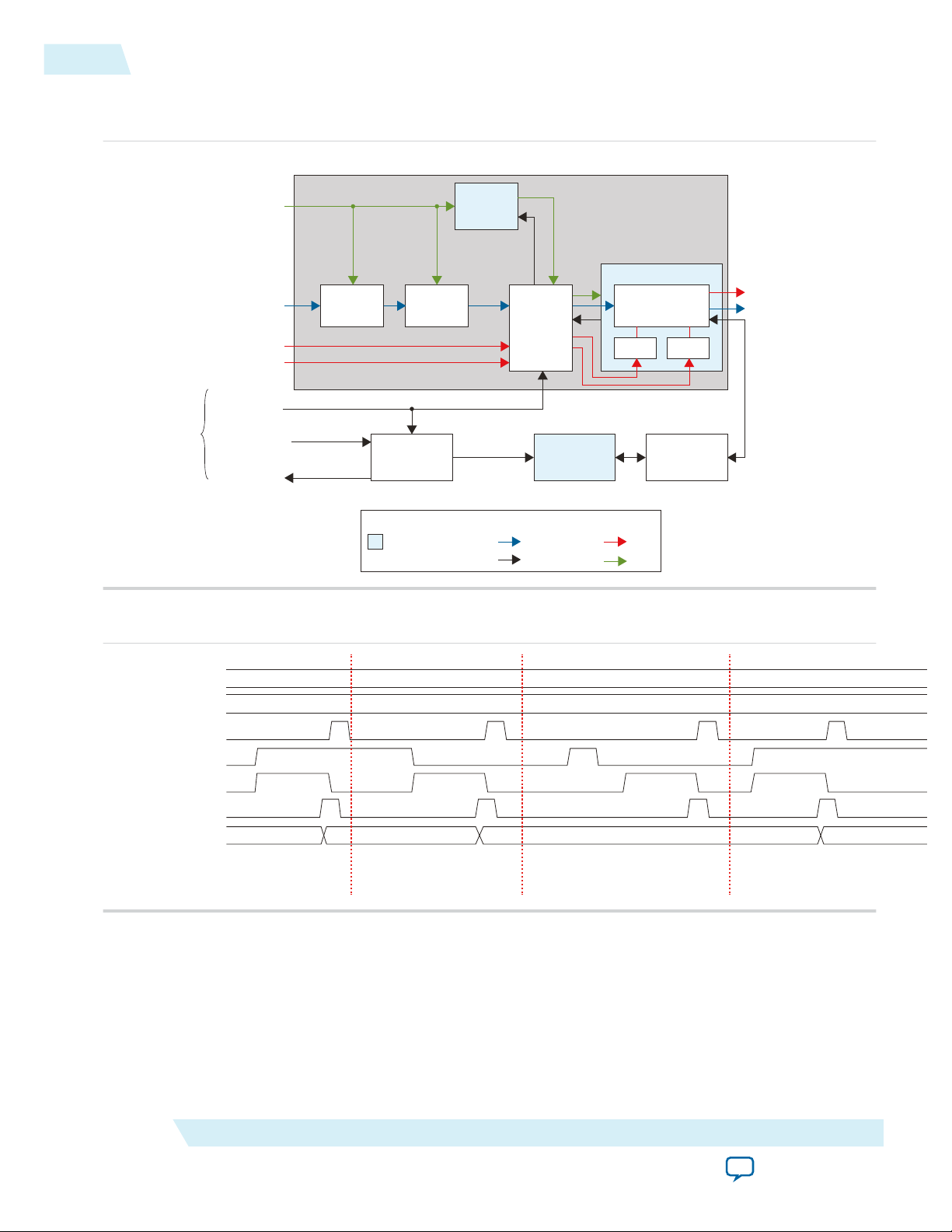
Design Examples for Arria 10 Devices
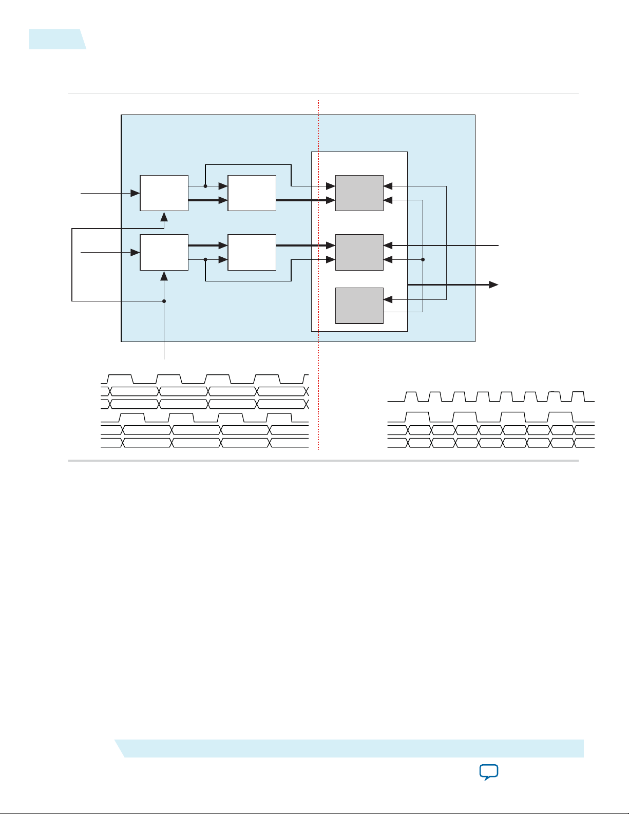
The figure below illustrates the generated design example entity and simulation testbench for Arria 10
devices. This design example consists of two SDI channels, a video pattern generator, a reconfiguration
controller, and a loopback path.
The IP core configures the device under test (DUT) block according to your parameterization. For
example, if you choose to generate an SDI RX, the software instantiates an SDI TX block to serve as a
video source.
The loopback block (SDI duplex) is always instantiated in the design example for parallel loopback
demonstrations.
The PHY adapter in the generated example design is not included in the figure below so that you can
observe how the signals are physically connected without the adapter. You may bypass the adapter in your
own design to make the design simpler.
For Arria 10 devices, the transceiver is no longer wrapped inside the IP core, and the TX PLL is no longer
wrapped inside the Transceiver PHY. You must generate these blocks separately in the example design.
SDI II IP Core Getting Started
Send Feedback
Altera Corporation
Page 25
Loopback
Path
Ch0 Loopback
(SDI TX + RX)
Arria 10 Native
PHY (Duplex)
Ch0 RX
Transceiver
Reset Controller
Pattern
Generator
Ch1 DUT
(SDI TX)
Arria 10 Native
PHY (TX)
Ch1 RX
Transceiver
Reset Controller
Ch0 TX
Transceiver
Reset Controller
Ch1 TX
Transceiver
Reconfiguration
Controller
Ch0 TX
PLL
Ch1 Test
(SDI RX)
Arria 10 Native
PHY (RX)
Ch0 TX
Transceiver
Reset Controller
Ch0 Duplex
Transceiver
Reconfiguration
Controller
Ch0 TX
PLL
Ch1 RX
Transceiver
Reconfiguration
Controller
TX Checker
RX
Checker
Test
Control
Testbench
Example Design
Data
Control
SDI II IP Core
Arria 10 Native PHY IP Core
Transceiver PHY Reset Controller IP Core
Arria 10 Transceiver CMU/ATX PLL IP Core
3-10
Design Examples for Arria 10 Devices
Figure 3-1: Design Example Entity and Simulation Testbench for Arria 10 Devices
UG-01125
2015.05.04
Altera Corporation
SDI II IP Core Getting Started
Send Feedback
Page 26

UG-01125
2015.05.04
This design generates two transceiver PHY reset controllers—one for TX and one for RX. These reset
controllers are connected to the transceiver to control the reset sequence. The PHY adapter controls the
rx_manual and rx_is_lockedtodata input signals of the reset controller. If you want to bypass the PHY
adapter, you must copy the assignment of these input signals in the sdi_ii_phy_adapter.v file to your design.
The table below describes how you should connect the input signals.
Table 3-4: Connecting Input Signals
Input Signal Connection
rx_manual Connect this signal to the rx_ready port of the PHY reset controller to
rx_is_lockedtodata Connect this signal to an output from a multiplexer between rx_is_
Note: The Transceiver Reconfiguration Controller that was used in the design examples for Arria V,
Cyclone V, and Stratix V devices are not applicable for Arria 10 devices. The reconfiguration
interface is now integrated into the transceiver. Each transceiver should pair with a reconfiguration
controller if it requires reconfiguration.
Design Examples for Arria V, Cyclone V, and Stratix V Devices
avoid any disturbance from short interference after the receiver is
locked.
lockedtoref and rx_is_lockedtodata ports from the transceiver,
with the rx_set_locktoref acting as the selector. The receiver operates
in locktoref mode when it receives SD video data. rx_is_lockedto-
data is not stable in this mode.
3-11
Design Examples for Arria V, Cyclone V, and Stratix V Devices
Figure below illustrates the generated design example entity and simulation testbench for Arria V,
Cyclone V, and Stratix V devices. This design example consists of a video pattern generator, transceiver
reconfiguration controller, reconfiguration management, loopback path, and various SDI blocks
occupying two transceiver channels.
SDI II IP Core Getting Started
Send Feedback
Altera Corporation
Page 27
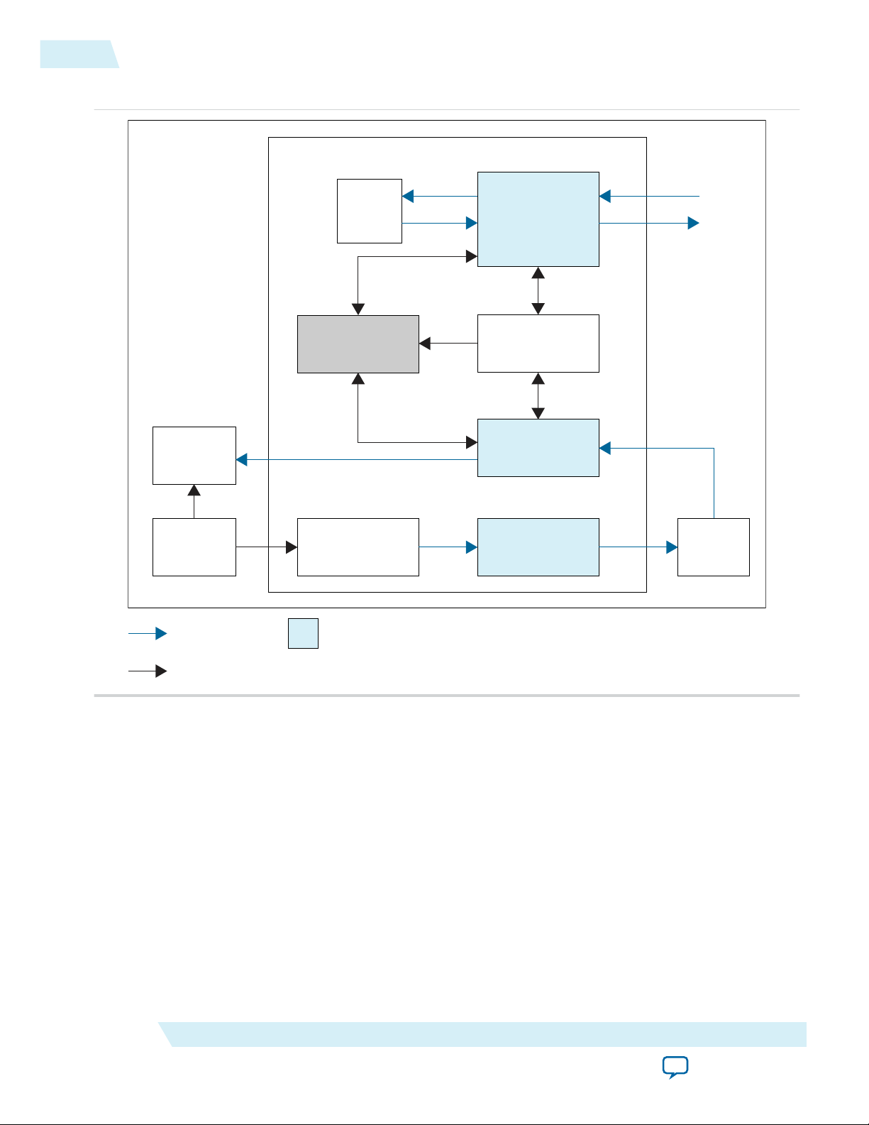
Loopback
Path
Ch0
Loopback
(SDI Duplex)
Reconfiguration
Management/Router
Ch1 Test
(SDI RX)
Ch1 DUT
(SDI TX)
Transceiver
Reconfiguration
Controller
Video Pattern
Generator
TX
Checker
RX
Checker
Test
Control
Data
Control
SDI II IP Core
Design Example
Testbench
3-12
Design Examples for Arria V, Cyclone V, and Stratix V Devices
Figure 3-2: Design Example Entity and Simulation Testbench
UG-01125
2015.05.04
Altera Corporation
SDI II IP Core Getting Started
Send Feedback
Page 28

Loopback
Path
Ch0
Loopback
(SDI Duplex)
Reconfiguration
Management/Router
Ch1 Test
(HD DL SDI TX)
Ch1 DUT
(HD DL SDI RX)
A to B
Video Pattern
Generator
Test
Control
Ch2 Test
(3-Gb SDI TX)
Ch2 Test
(3-Gb SDI RX)
TX
Checker
RX
Checker
Loopback
Path
Data
Control
SDI II IP Core
Design Example
Testbench
Transceiver
Reconfiguration
Controller
UG-01125
2015.05.04
Design Examples for Arria V, Cyclone V, and Stratix V Devices
Figure 3-3: Design Example Entity and Simulation Testbench for HD-SDI Dual Link to 3G-SDI (Level B)
Conversion
The figure below illustrates the generated design example entity and simulation testbench when you
generate HD-SDI dual link receiver with Convert HD-SDI dual link to 3G-SDI (level B) option enabled.
3-13
SDI II IP Core Getting Started
Send Feedback
Altera Corporation
Page 29

Loopback
Path
Ch0
Loopback
(SDI Duplex)
Reconfiguration
Management/Router
Ch1 Test
(3-Gb SDI TX)
Ch1 DUT
(3-Gb SDI RX)
B to A
Video Pattern
Generator
Test
Control
Ch2 Test
(HD DL SDI TX)
Ch2 Test
(HD DL SDI RX)
TX
Checker
RX
Checker
Loopback
Path
Data
Control
SDI II IP Core
Design Example
Testbench
Transceiver
Reconfiguration
Controller
3-14
Design Example Components
Figure 3-4: Design Example Entity and Simulation Testbench for 3G-SDI (Level B) to HD-SDI Dual Link
Conversion
The figure below illustrates the generated design example entity and simulation testbench when you
generate 3G-SDI or triple rate SDI receiver with Convert 3G-SDI (level B) to HD-SDI dual link option
enabled.
UG-01125
2015.05.04
Design Example Components
The Arria V, Cyclone V, and Stratix V design examples for the SDI II IP core consist of the following
components:
• Video pattern generator
• Transceiver reconfiguration controller
• Reconfiguration management
• Reconfiguration router
Altera Corporation
SDI II IP Core Getting Started
Send Feedback
Page 30

UG-01125
2015.05.04
Video Pattern Generator
The Arria 10 design example for the SDI II IP core consists of the following components:
• Video pattern generator
• Transceiver reconfiguration controller
Video Pattern Generator
The video pattern generator generates a colorbar or pathological pattern. The colorbar is preferable for
image generation while the pathological pattern can stress the PLL and cable equalizer of the attached
video equipment. You can configure the video pattern generator to generate various video formats.
Table 3-5: Configuring the Video Pattern Generator to Generate Different Video Formats
Table below lists the examples of how to configure the video pattern generator signals to generate a video format
that you desire.
Example
Video
Format
Interface
pattgen_tx_std pattgen_tx_format pattgen_dl_mapping
Signal
3-15
Example 1:
Generate
1080i video
format
1080i60 HD-SDI 2'b01 4'b0100 1'b0
1080i60x2
HD-SDI
dual link
2'b01 4'b0100 1'b0
3Gb 2'b10 4'b0100 1'b0
1080p30 HD-SDI 2'b01 4'b1100 1'b0
Example 2:
Generate
1080p
video
format
1080p30x2 HD-SDI
dual link
HD-SDI
dual link
1080p60
3Ga 2'b11 4'b1100 1'b0
2'b01 4'b1100 1'b0
2'b01 4'b1100 1'b1
3Gb 2'b10 4'b1100 1'b1
Related Information
Video Pattern Generator Signals on page 3-22
Transceiver Reconfiguration Controller
The transceiver reconfiguration controller reconfigures the transceivers. The transceiver reconfiguration
controller in the Arria V, Cyclone V, and Stratix V design examples and the Arria 10 design example is
used differently.
Related Information
• Transceiver Reconfiguration Controller Signals on page 3-23
• Modifying the Transceiver Reconfiguration Controller on page 3-19
Transceiver Reconfiguration Controller for Arria 10
For Arria 10 design examples, the reconfiguration interface is integrated into the Arria 10 Native PHY
instance and TX PLL. Each transceiver and PLL contains an Avalon-MM reconfiguration interface that
must be connected to this reconfiguration controller user logic.
SDI II IP Core Getting Started
Send Feedback
Altera Corporation
Page 31

3-16
Transceiver Reconfiguration Controller for Arria V, Cyclone V, and...
Transceiver Reconfiguration Controller for Arria V, Cyclone V, and Stratix V
For Arria V, Cyclone V, and Stratix V design examples, the transceiver reconfiguration controller allows
you to change the device transceiver settings at any time. Any portion of the transceiver can be selectively
reconfigured. Each portion of the reconfiguration requires a read-modify-write operation (read first, then
write), in such a way by modifying only the appropriate bits in a register and not changing other bits.
Prior to this operation, you must define the logical channel number and the streamer module mode.
You can perform a transceiver dynamic reconfiguration in these two modes:
• streamer module mode 1 (manual mode)—execute a series of Avalon® Memory-Mapped (AvalonMM) write operation to change the transceiver settings. In this mode, you can execute a write
operation directly from the reconfiguration management/router interface to the device transceiver
registers.
• streamer module mode 0—use the .mif files to change the transceiver settings.
For read operation, after defining the logical channel number and the streamer module mode, the
following sequence of events occur:
1. Define the transceiver register offset in the offset register.
2. Read the data register. Toggle the read process by setting bit 1 of the control and status register (CSR)
to logic 1.
3. Once the busy bit in the CSR is cleared to logic 0, it indicates that the read operation is complete and
the required data should be available for reading.
UG-01125
2015.05.04
For write operation, after setting the logical channel number and the streamer module mode, the
following sequence of events occur:
1. Define the transceiver register offset (in which the data will be written to) in the offset register.
2. Write the data to the data register. Toggle the write process by setting bit 0 of the CSR to logic 1.
3. Once the busy bit in the CSR is cleared to logic 0, it indicates that the transceiver register offset
modification is successful.
For more information about the transceiver reconfiguration controller streamer module, refer to the
Transceiver Reconfiguration Controller IP Core Overview chapter of the Altera Transceiver PHY IP Core
User Guide.
Related Information
Altera Transceiver PHY IP Core User Guide
More information about the transceiver reconfiguration controller streamer module.
Reconfiguration Management
The reconfiguration management block (sdi_ii_ed_reconfig_mgmt.v and sdi_ii_reconfig_logic.v) contains the
reconfiguration user logic (a finite state machine) to determine the bits that needs to be modified, and
selects the correct data to be written to the appropriate transceiver register through streamer module
mode 1. It also provides handshaking between the SDI receiver and the transceiver reconfiguration
controller. In this design, each reconfiguration block must interface with only one transceiver reconfigu‐
ration controller.
During the reconfiguration process, the logic first reads the data from the transceiver register that needs
to be reconfigured and stores the data temporarily in a local register. Then, the logic overwrites only the
appropriate bits of the data with predefined values and write the modified data to the transceiver register.
Altera Corporation
SDI II IP Core Getting Started
Send Feedback
Page 32

UG-01125
2015.05.04
Since only one transceiver register can be accessed at a time, the whole process repeats when reconfi‐
guring other registers.
For multiple SDI channels reconfiguration, the logical channel number needs to be set appropriately for
each channel and reconfiguration interface. For example, in the design example and simulation testbench
figure, there are one SDI duplex, one SDI RX, and one SDI TX block. The number of reconfiguration
interface for SDI duplex is 2 (one for channel and one for TX PLL), for SDI RX is 1 (for channel), for SDI
TX is 2 (one for channel and one for TX PLL). The total number of reconfiguration interface required in
the transceiver reconfiguration controller is 5.
The table below lists the channel and transceiver reconfiguration controller interface numbers.
The logical channel number for the receiver in SDI duplex is 0 and the logical channel number for SDI RX
is 2. The generated example design entity demonstrates this interface connection.
Table 3-6: Channel Numbers Setting for Multiple SDI Channels Reconfiguration
SDI Block SDI Channel Number Transceiver Reconfiguration Controller Interface Number
SDI Duplex 0 0 and 1
SDI RX 1 2
SDI TX 1 3 and 4
Reconfiguration Router
3-17
For more information about the logical channel number, refer to the Transceiver Reconfiguration
Controller IP Core Overview chapter of the Altera Transceiver PHY IP Core User Guide.
Related Information
• Reconfiguration Management Parameters on page 3-26
Table below lists the parameters for reconfiguration management.
• Modifying the Reconfiguration Management on page 3-20
• Altera Transceiver PHY IP Core User Guide
For more information about the logical channel number.
Reconfiguration Router
The reconfiguration router (sdi_ii_ed_reconfig_router.v) connects multiple SDI instances to the reconfigu‐
ration management and transceiver reconfiguration controller blocks. The reconfiguration router receives
all the interface signals between the transceiver reconfiguration controller and reconfiguration
management, as well as SDI instances, and transmits the signals to their respective destinations.
The reconfiguration router converts reconfiguration related interface signals of multiple SDI instances
and user interface to a single-wide data bus for the reconfiguration management and transceiver reconfi‐
guration controller blocks. You can bypass this component if you want to implement designs that expands
to more channels. The details are described in the Expanding to Multiple Channels section.
Related Information
• Reconfiguration Router Signals on page 3-27
Table below lists the signals for the reconfiguration router.
• Modifying the Reconfiguration Router on page 3-21
SDI II IP Core Getting Started
Send Feedback
Altera Corporation
Page 33

3-18
Avalon-MM Translators
Avalon-MM Translators
The Avalon-MM Master Translator and Avalon-MM Slave Translator are Avalon-MM interface blocks
that access the Transceiver Reconfiguration Controller registers. The translators are not SDI-specific and
are automatically instantiated when the core interfaces with an Avalon-MM master or slave component.
If you want to bypass the Avalon MM translator in your design, connect reconfig_mgmt_address[8:2]
from the reconfiguration management block to reconfig_mgmt_address from the Transceiver Reconfi‐
guration Controller.
You can connect the other signals from the reconfiguration management block directly to the Transceiver
Reconfiguration Controller.
• reconfig_mgmt_waitrequest
• reconfig_mgmt_read
• reconfig_mgmt_readdata
• reconfig_mgmt_write
• reconfig_mgmt_writedata
For more information about the Avalon-MM Translator functions, refer to the Qsys Interconnect chapter
in volume 1 of the Quartus II Handbook.
Related Information
UG-01125
2015.05.04
• Qsys Interconnect
More information about the Avalon-MM Translator functions.
• Avalon Interface Specifications
Transceiver Dynamic Reconfiguration
The dual and triple standard SDI receivers (or receivers of duplex SDIs) require the transceiver dynamic
reconfiguration feature to perform auto detection and locking to different SDI video rates. Transceiver
dynamic reconfiguration reconfigures the transceivers to support the three SDI video standards (SD, HD
and 3G).
You need to perform transceiver dynamic reconfiguration on the SDI transmitter (or transmitters
Note:
of duplex SDIs) if you want to use the dynamic TX clock switching feature.
The dual and triple standard SDI use 11 times oversampling for receiving SD-SDI standard. As the rates
for 3G-SDI and SD-SDI are the same, transceiver reconfiguration is not required when the video standard
changes from 3G-SDI to SD-SDI and vice versa. Transceiver reconfiguration is only required when the
video standard changes from 3G-SDI or SD-SDI to HD-SDI, and vice versa.
To perform transceiver dynamic reconfiguration, you need the transceiver reconfiguration controller and
reconfiguration management/router blocks.
Altera Corporation
SDI II IP Core Getting Started
Send Feedback
Page 34

UG-01125
2015.05.04
The following sequence of events occur when there is a change in the SDI receiver video standard:
1. The SDI receiver locks to 3G-SDI standard and detects the incoming video standard has changed from
3G-SDI to HD-SDI. The transceiver controller requests a reconfiguration.
2. The transceiver reconfiguration controller determines the appropriate settings to write based on the
information from the transceiver controller. Then, it performs the read-modify-write operation to
reconfigure the device transceiver.
3. Once the reconfiguration completes, the transceiver reconfiguration controller indicates to the SDI
receiver that reconfiguration is complete.
4. The SDI receiver begin the process of locking to the incoming data.
Expanding to Multiple Channels
The generated design example consists of two SDI channels, where the SDI duplex instance always occupy
Channel 0 (Ch0), while the SDI instance at Channel 1 (Ch1) depends on your selection from the
parameter editor. To expand and accommodate more channels, you must perform some modifications to
the source files.
For example, when Ch0 is duplex, Ch1 is RX and TX, if you want to instantiate an additional SDI duplex
instance at Channel 2 (Ch2), you need to make some modifications to the following components.
Note: This is only applicable for Arria V, Cyclone V, and Stratix V design examples. For Arria 10 design
example, just duplicate another transceiver reconfiguration controller generated from the example
design for the additional channel.
Expanding to Multiple Channels
3-19
Modifying the Transceiver Reconfiguration Controller
Perform the following changes to modify the transceiver reconfiguration controller:
• Edit the Number_of_reconfig_interfaces parameter. This parameter specifies the total number of
reconfiguration interfaces that connect to this block.
• Each channel or TX PLL needs one reconfiguration interface. Therefore, an SDI duplex or SDI TX
mode requires two interfaces while an SDI RX mode requires only one interface. If you enable the
dynamic TX clock switching feature, , the SDI duplex or SDI TX mode requires three interfaces. The
additional interface is for the additional TX PLL. For simplicity, assume this option is disabled.
• Determine the total number of reconfiguration interfaces required in your design and assign the
parameter value accordingly. In this design example, the total number of reconfiguration interfaces is 7
(Ch0=2, Ch1=3 and Ch2=2).
• Link the reconfig_to_xcvr and reconfig_from_xcvr signals from the additional SDI duplex
instance at Ch2. You must link the signals in the order of the logical channel number (rx_log_ch_num
and tx_log_ch_num) in the reconfiguration logic source file (sdi_ii_reconfig_logic.v).
• In the design example that instantiates the transceiver reconfiguration controller, add the wire
connection between the additional SDI duplex instance at Ch2 and the transceiver reconfiguration
controller as shown below:
wire [ 139:0] reconfig_to_xcvr_du_ch2;
wire [ 91:0] reconfig_from_xcvr_du_ch2;
wire [ 139:0] reconfig_to_xcvr_tx_ch1;
wire [ 69:0] reconfig_to_xcvr_rx_ch1;
wire [ 91:0] reconfig_from_xcvr_tx_ch1;
wire [ 45:0] reconfig_from_xcvr_rx_ch1;
wire [ 139:0] reconfig_to_xcvr_du_ch0;
wire [ 91:0] reconfig_from_xcvr_du_ch0;
alt_xcvr_reconfig #(
SDI II IP Core Getting Started
Send Feedback
Altera Corporation
Page 35

3-20
Modifying the Reconfiguration Management
.number_of_reconfig_interfaces (7),
….
) u_reconfig (
.reconfig_to_xcvr ({reconfig_to_xcvr_du_ch2,
reconfig_to_xcvr_tx_ch1,
reconfig_to_xcvr_rx_ch1,
reconfig_to_xcvr_du_ch0}),
.reconfig_from_xcvr ({reconfig_from_xcvr_du_ch2,
reconfig_from_xcvr_tx_ch1,
reconfig_from_xcvr_rx_ch1,
reconfig_from_xcvr_du_ch0}),
);
Modifying the Reconfiguration Management
Perform the following changes to modify the reconfiguration management:
• Edit the Number_of_channels parameter in sdi_ii_ed_reconfig_mgmt.v. This parameter value should be
the total number of the SDI RX channels declared in the design. In this example, the NUM_CHS is 3.
• Link the interface signals—sdi_rx_start_reconfig, sdi_rx_reconfig_done, and sdi_rx_std—
between multiple SDI instances and reconfiguration management block. Link the interface signals—
sdi_tx_start_reconfig, sdi_tx_reconfig_done, and sdi_tx_pll_sel—between user and reconfi‐
guration management block. You must link the signals in the order of the logical channel number
(rx_log_ch_num and tx_log_ch_num) in the reconfiguration logic source file (sdi_ii_reconfig_logic.v).
For example:
UG-01125
2015.05.04
wire tx_start_reconfig_ch2,tx_start_reconfig_ch1,tx_start_reconfig_ch0;
wire tx_pll_sel_ch2,tx_pll_sel_ch1,tx_pll_sel_ch0;
wire tx_reconfig_done_ch2,tx_reconfig_done _ch1,tx_reconfig_done_ch0;
wire rx_start_reconfig_ch2,rx_start_reconfig_ch1,rx_start_reconfig_ch0;
wire [1:0] rx_std_ch2, rx_std_ch1,rx_std_ch0;
wire rx_reconfig_done_ch2,rx_reconfig_done _ch1,rx_reconfig_done_ch0;
sdi_ii_ed_reconfig_mgmt #(
. NUM_CHS (3),
) u_reconfig_mgmt (
.sdi_tx_start_reconfig (tx_start_reconfig_ch2,
tx_start_reconfig_ch1,tx_start_reconfig_ch0),
.sdi_tx_pll_sel (tx_pll_sel_ch2,tx_pll_sel_ch1,tx_pll_sel_ch0),
.sdi_tx_reconfig_done (tx_reconfig_done_ch2,
tx_reconfig_done_ch1,tx_reconfig_done_ch0),
.sdi_rx_start_reconfig (rx_start_reconfig_ch2,
rx_start_reconfig_ch1,rx_start_reconfig_ch0),
.sdi_rx_std (rx_std_ch2,rx_std_ch1,rx_std_ch0),
.sdi_rx_reconfig_done (rx_reconfig_done_ch2,
rx_reconfig_done_ch1,rx_reconfig_done_ch0)
)
• In the reconfiguration logic source file, the default setting for the wire rx_log_ch_num is 0 and 2 for
channel 0 and channel 1, respectively. The default setting for the wire tx_log_ch_num is 0 and 2
(duplex) or 3 (TX) for channel 0 and channel 1, respectively. These numbers are referring to the
Number_of_channels parameter value that was set in transceiver reconfiguration controller. Hence,
the logical channel number for each SDI channel is as listed in the table below.
Altera Corporation
SDI II IP Core Getting Started
Send Feedback
Page 36

UG-01125
2015.05.04
Table 3-7: Logical Channel Number For Each SDI Channel
Modifying the Reconfiguration Router
3-21
SDI Channel Direction Number of Reconfiguration
Logical Channel Number
Interfaces
0 Duplex 2 • 0: RX/TX channel
• 1: Tx PLL
1 RX and TX 3 (1 for RX and 2 for TX) • 2: RX channel
• 3: TX channel
• 4: TX PLL
2 Duplex 2 • 5: RX/TX channel
• 6: TX PLL
• Edit the reconfiguration logic source file to assign the logical channel number for the additional SDI
duplex instance, which occupies the SDI Ch2. The logical channel number specified in the source file is
the reconfiguration interface that is intended for dynamic reconfiguration. For example, if TX channel
is intended for dynamic reconfiguration, tx_log_ch_num[2] should be 5.
wire [7:0] rx_log_ch_num [0:NUM_CHS-1];
assign rx_log_ch_num[0] = 8'd0; // Duplex Rx channel share same
logical channel number with Tx
assign rx_log_ch_num[1] = 8'd2; // Rx channel
assign rx_log_ch_num[2] = 8'd5; // Duplex Rx channel
wire [7:0] tx_log_ch_num [0:NUM_CHS-1];
assign tx_log_ch_num[0] = 8'd0; // Duplex Tx channel share same
logical channel number with Rx
assign tx_log_ch_num[1] = 8'd3; // Tx channel
assign tx_log_ch_num[2] = 8'd5; // Duplex Tx channel
Related Information
Altera Transceiver PHY IP Core User Guide
More information about the transceiver reconfiguration controller logical channel numbering.
Modifying the Reconfiguration Router
For ease of implementation, you can bypass this block by connecting the interface signals—
reconfig_to_xcvr, reconfig_from_xcvr, sdi_rx_start_reconfig, sdi_rx_reconfig_done,
sdi_rx_std, sdi_tx_start_reconfig, sdi_tx_reconfig_done, and sdi_tx_pll_sel—directly
SDI II IP Core Getting Started
Altera Corporation
Send Feedback
Page 37

3-22
Video Pattern Generator Signals
UG-01125
2015.05.04
between the SDI instance and the transceiver reconfiguration controller or the reconfiguration
management.
Video Pattern Generator Signals
Table 3-8: Video Pattern Generator Top Level Signals
Table below lists the input signals for the video pattern generator. The listed signals are exported at the top level of
the design example. Other signals—that are not exported—connect within the design example entity.
Signal Width Direction Description
pattgen_tx_std
pattgen_tx_format
2 Input Transmit video standard.
• 00: SD-SDI
• 01: HD-SDI or HD-SDI dual link
• 10: 3G-SDI level B
• 11: 3G-SDI level A
4 Input Transmit video format.
• 0000: SMPTE259M 525i
• 0001: SMPTE259M 625i
• 0100: SMPTE274M 1080i60
• 0101: SMPTE274M 1080i50
• 0110: SMPTE274M 1080p24
• 0111: SMPTE296M 720p60
• 1000: SMPTE296M 720p50
• 1001: SMPTE296M 720p30
• 1010: SMPTE296M 720p25
• 1011: SMPTE296M 720p24
• 1100: SMPTE274M 1080p30
• 1101: SMPTE274M 1080p25
• 1110: SMPTE274M 1080sF24
• Others: Reserved for future use
pattgen_dl_mapping
pattgen_ntsc_paln
pattgen_bar_100_75n
Altera Corporation
1 Input Dual link mapping. Set to 1 for HD-SDI dual link
and 3Gb transmit video standard only.
1 Input Transmit rate.
• 0: PAL (1) rate. For example, 1080p30
• 1: NTSC (1/1.001) rate. For example,
1080p29.97.
This input ignores all SD video formats (525i, 625i)
and certain HD video formats that do not support
NTSC rate (1080i50, 720p50, 720p25, 1080p25).
1 Input Generate color bars.
• 0: 75% color bars
• 1: 100% color bars
SDI II IP Core Getting Started
Send Feedback
Page 38

UG-01125
2015.05.04
Transceiver Reconfiguration Controller Signals
Signal Width Direction Description
3-23
pattgen_patho
pattgen_blank
pattgen_no_color
pattgen_sgmt_frame
1 Input Set to 1 to generate pathological pattern.
1 Input Set to 1 to generate black signal.
1 Input Set to 1 to generate bars with no color.
1 Input Set to 1 to generate segmented frame picture for tx_
format:
• 0100: SMPTE274M 1080sF30
• 0101: SMPTE274M 1080sF25
Related Information
Video Pattern Generator on page 3-15
Transceiver Reconfiguration Controller Signals
Table 3-9: Transceiver Reconfiguration Controller Signals for Arria V, Cyclone V, and Stratix V Devices
Table below lists the input signals for the transceiver reconfiguration controller. The listed signals are exported at
the top level of the design example. Other signals—that are not exported—connects within the design example
entity.
Signal Width Direction Description
reconfig_clk
1
Clock signal for the transceiver reconfigura‐
tion controller and reconfiguration
Input
management/router. Refer to the transceiver
reconfiguration controller section in the
Altera Transceiver PHY IP User Guide for
information about the frequency range.
reconfig_rst
1
Input
Reset signal for the transceiver reconfigura‐
tion controller and reconfiguration
management/router. This signal is active high
and level sensitive.
Table 3-10: Transceiver Reconfiguration Controller Signals for Arria 10 Devices
The table below describes the signals available for the reconfiguration controller.
Signal Width Direction Description
xcvr_reconfig_clk 1 Input Clock signal for reconfiguration user logic.
This clock must share the same clock source
as reconfig_clk in the transceiver.
SDI II IP Core Getting Started
Send Feedback
Altera Corporation
Page 39

3-24
Transceiver Reconfiguration Controller Signals
Signal Width Direction Description
xcvr_reconfig_rst 1 Input Reset signal for reconfiguration user logic.
This signal is active high and level sensitive.
This reset signal must share the same reset
source as reconfig_reset in the transceiver.
xcvr_reconfig_write 1 Output Write enable signal.
Connect this signal to reconfig_write in the
transceiver.
xcvr_reconfig_read 1 Output Read enable signal.
Connect this signal to reconfig_read in the
transceiver.
xcvr_reconfig_address 10 Output Reconfiguration address.
Connect this signal to reconfig_address in
the transceiver.
xcvr_reconfig_writedata 32 Output A 32-bit data write bus.
UG-01125
2015.05.04
Connect this bus to reconfig_writedata in
the transceiver.
xcvr_reconfig_readdata 32 Input A 32-bit data read bus. This signal returns
valid data from the transceiver after a read
operation.
Connect this bus to reconfig_readdata in
the transceiver.
xcvr_reconfig_waitrequest 1 Input Status signal from the transceiver that
indicates that the Avalon-MM interface is
busy.
Connect this signal to reconfig_
waitrequest in the transceiver.
cdr_reconfig_sel 2 Input Signal to specify which data rate the CDR
should be configured to.
Connect this signal to rx_std in the SDI II
IP core.
cdr_reconfig_req 1 Input Request signal to start the CDR dynamic
reconfiguration.
Connect this signal to rx_sdi_start_
reconfig in the SDI II IP core.
cdr_reconfig_busy 1 Output Status signal that indicates that CDR reconfi‐
Altera Corporation
guration is taking place.
Connect this signal to rx_sdi_reconfig_
done in the SDI II IP core.
SDI II IP Core Getting Started
Send Feedback
Page 40

UG-01125
2015.05.04
Transceiver Reconfiguration Controller Signals
Signal Width Direction Description
pll_sel 1 Input Signal to specify which TX PLL to use. This
signal must share the same source as pll_
select signal in the transceiver PHY reset
controller.
pll_sw_req 1 Input Request signal to start the PLL switching
dynamic reconfiguration.
Note: Do not assert this signal when
other reconfiguration signals are
busy, for example cdr_reconfig_
busy.
pll_busy 1 Output Status signal that indicates that the PLL
switching process is taking place.
external_avmm_master_req 1 Input Request signal from the external Avalon-MM
master. Tie this signal to 0 if you do not use
the external Avalon-MM master.
3-25
reconfig_write_from_ext_
avmm_master
reconfig_read_from_ext_
avmm_master
reconfig_address_from_ext_
avmm_master
reconfig_writedata_from_
ext_avmm_master
reconfig_readdata_from_ext_
avmm_master
reconfig_waitrequest_from_
ext_avmm_master
1 Input Write enable signal. Connect this signal to the
write signal of the external Avalon-MM
master if you have one in your design.
1 Input Read enable signal. Connect this signal to the
read signal of the external Avalon-MM
master if you have one in your design.
10 Input Reconfiguration address. Connect this signal
to the reconfig address bus of the external
Avalon-MM master if you have one in your
design.
32 Input A 32-bit data write bus. Connect this bus to
the reconfig data write bus of the
external Avalon-MM master if you have one
in your design.
32 Output A 32-bit data read bus. Connect this bus to
the reconfig data read bus of the external
Avalon-MM master if you have one in your
design.
1 Output
Status signal that indicates that the AvalonMM is busy. Connect this signal to the
waitrequest signal of the external Avalon-
MM master if you have one in your design.
SDI II IP Core Getting Started
Send Feedback
Note: Do not issue any Avalon
commands when this signal is
high.
Altera Corporation
Page 41

3-26
Reconfiguration Management Parameters
Related Information
• Transceiver Reconfiguration Controller on page 3-15
The transceiver reconfiguration controller reconfigures the transceivers. The transceiver reconfiguration
controller in the Arria V, Cyclone V, and Stratix V design examples and the Arria 10 design example is
used differently.
• Modifying the Transceiver Reconfiguration Controller on page 3-19
• Altera Transceiver PHY IP Core User Guide
More information about the transceiver reconfiguration controller frequency range.
Reconfiguration Management Parameters
Table below lists the parameters for reconfiguration management.
Table 3-11: Reconfiguration Management Parameters
Parameter Value Description
NUM_CHS 1 (minimum) Number of channels required to do reconfiguration
UG-01125
2015.05.04
FAMILY
DIRECTION
VIDEO_STANDARD
XCVR_TX_PLL_SEL
• Arria V
• Arria V GZ
• Cyclone V
• Stratix V
• tx
• rx
• du
• tr
• dl
• 1
• 2
Supported device family
Direction of the core selected in the parameter
editor. This parameter affects the logical channel
number assigned in the generated example design.
If you are making any changes to the design, please
ignore this parameter and assign the logical channel
number correctly.
Refer to Expanding to Multiple Channels section to
know how to assign the logical channel number.
Current video standard.
Specify dl for HD dual-link or tr for other
standards.
The selected method to perform TX PLL reconfigu‐
ration for dynamic clock switching. Specify 1 to
switch TX PLLs or 2 to switch TX PLL reference
clocks.
Altera Corporation
The specified value must match the parameter value
you select when you instantiate the core.
Refer to Dynamic TX Clock Switching section to
know more about clock switching.
SDI II IP Core Getting Started
Send Feedback
Page 42

UG-01125
2015.05.04
Related Information
Reconfiguration Router Signals
• Reconfiguration Management on page 3-16
• Modifying the Reconfiguration Management on page 3-20
Reconfiguration Router Signals
Table below lists the signals for the reconfiguration router.
Table 3-12: Reconfiguration Router Top Level Signals
The listed signals are exported at the top level of the design example. Other signals—that are not exported—
connect within the design example entity.
Note: These signals are available only when you use the Dynamic TX clock switching feature.
Refer to Dynamic TX Clock Switching for usage requirements.
3-27
Signal Width Directio
ch1_<direction>_tx_start_reconfig
ch1_<direction>_tx_pll_sel
ch1_<direction>_tx_reconfig_done
Related Information
1 Input Dynamic reconfiguration request signal
1 Input TX PLL select signal for TX PLL dynamic
1 Output Dynamic reconfiguration acknowledge
• Reconfiguration Router on page 3-17
• Modifying the Reconfiguration Router on page 3-21
Description
n
for TX PLL dynamic switching at
transmitter or duplex instance at channel
1.
switching at transmitter or duplex
instance at channel 1. This signal is also
connected to xcvr_refclk_sel signal of
the SDI instance.
signal for TX PLL dynamic switching at
transmitter or duplex instance at channel
1.
SDI II IP Core Getting Started
Send Feedback
Altera Corporation
Page 43

2015.05.04
Transceiver
SDI II IP Core
Parallel Video In
Parallel Video Out
SDI Out
SDI In
20
20
20
20
Protocol
PHY Management
& PHY Adapter
Hard Transceiver
www.altera.com
101 Innovation Drive, San Jose, CA 95134
SDI II IP Core Functional Description
4
UG-01125
Subscribe
Send Feedback
The SDI II IP core implements a transmitter, receiver, or full-duplex interface.
The SDI II IP core consists of the following components:
• Protocol block—transmitter or receiver
• Transceiver blocks—PHY management & adapter and hard transceiver
In the parameter editor, you can specify either protocol, transceiver, or combined blocks for your design.
For example, if you have multiple protocol blocks in a design, you can multiplex them into one
transceiver.
The modular hierarchy design allows you to remove or reuse each submodule within the components
across different video standards. The transmitter and receiver data paths are independent from each
other.
The following figure shows the block diagram for non-Arria 10 devices.
Figure 4-1: SDI II IP Core Block Diagram for Arria V, Cyclone V, and Stratix V Devices
For the Arria 10 devices, the SDI II IP core no longer provides the transceiver, and the TX PLL is no
longer wrapped in the transceiver PHY. You must generate the transceiver and the TX PLL separately.
The figure below shows the block diagram for Arria 10 devices.
©
2015 Altera Corporation. All rights reserved. ALTERA, ARRIA, CYCLONE, ENPIRION, MAX, MEGACORE, NIOS, QUARTUS and STRATIX words and logos are
trademarks of Altera Corporation and registered in the U.S. Patent and Trademark Office and in other countries. All other words and logos identified as
trademarks or service marks are the property of their respective holders as described at www.altera.com/common/legal.html. Altera warrants performance
of its semiconductor products to current specifications in accordance with Altera's standard warranty, but reserves the right to make changes to any
products and services at any time without notice. Altera assumes no responsibility or liability arising out of the application or use of any information,
product, or service described herein except as expressly agreed to in writing by Altera. Altera customers are advised to obtain the latest version of device
specifications before relying on any published information and before placing orders for products or services.
ISO
9001:2008
Registered
Page 44

SDI II IP Core for Arria 10
Parallel Video In
Parallel Video Out
SDI Out
SDI In
Protocol
PHY Reset
Controller
TX PLL
Arria 10
Native PHY IP
4-2
Protocol
Figure 4-2: SDI II IP Core Block Diagram for Arria 10 Devices
Protocol
The protocol block handles the SDI-specific parts of the core and generally operates on a parallel domain
data.
UG-01125
2015.05.04
Transmitter
The transmitter performs the following functions:
• HD-SDI LN insertion
• Sync bit insertion
• HD-SDI CRC generation and insertion
• Payload ID insertion
• Matching timing reference signal (TRS) word
• Clock enable signal generation
• Scrambling and non-return-zero inverted (NRZI) coding
The block diagrams below illustrate the SDI II IP core transmitter (simplex) data path for each supported
video standard.
For more information about the function of each submodules, refer to the Submodules section.
Altera Corporation
SDI II IP Core Functional Description
Send Feedback
Page 45

Match
TRS
Insert
Payload ID
Scrambler
TX
Oversample
Generate
Clock Enable
Transmit
TX Protocol TX PHY Management
& PHY Adapter
Transceiver
Parallel
Video In
SDI Out
10 10 10 20
Match
TRS
Insert
Line
Scrambler
Insert
Line
20
Multiplexer
20
Transmit
TX Protocol
TX PHY
Management
& PHY Adapter
Transceiver
Parallel
Video In
10
SDI Out
10
Insert
CRC
Insert
CRC
10
Insert
Payload ID
10
10
10 10
20
Demultiplexer
Y
C
Scrambler
Insert
Line
20
Multiplexer
20
20
TX
Oversample
Generate
Clock Enable
TX PHY Management
& PHY Adapter
20 20
Transmit
TX Protocol Transceiver
Parallel
Video In
10
SDI Out
10
Insert
CRC
Insert
CRC
10
Insert
Payload ID
10
10
10 10
10
Insert
Payload ID
Demultiplexer
Y (HD)
C (HD)
Match
TRS
Convert
SD Bits
Insert
Line
UG-01125
2015.05.04
Figure 4-3: SD-SDI Transmitter Data Path Block Diagram
Figure 4-4: HD/3G-SDI Transmitter Data Path Block Diagram
Transmitter
4-3
Figure 4-5: Dual Rate SDI Transmitter Data Path Block Diagram
SDI II IP Core Functional Description
Send Feedback
Altera Corporation
Page 46

Match
TRS
Insert
Line
Scrambler
Insert
Line
Multiplexer
20
Transmit
TX Protocol
TX PHY
Management
& PHY Adapter
Transceiver
Parallel
Video In
Link A
10
SDI Out
Link A
10
Insert
CRC
Insert
CRC
10
Insert
Payload ID
10
10
10 10
Match
TRS
Insert
Line
Scrambler
Insert
Line
20
20
Multiplexer
20
Transmit
TX Protocol
Parallel
Video In
Link B
10
SDI Out
Link B
10
Insert
CRC
Insert
CRC
10
Insert
Payload ID
10
10
10 10
20
Demultiplexer
Y
C
20
Demultiplexer
Y
C
4-4
Transmitter
Figure 4-6: Dual Link HD-SDI Transmitter Data Path Block Diagram
UG-01125
2015.05.04
Altera Corporation
SDI II IP Core Functional Description
Send Feedback
Page 47

Match
TRS
Insert
Line
Scrambler
Insert
Line
20
Multiplexer
20
20
TX
Oversample
Generate
Clock Enable
TX PHY Management
& PHY Adapter
20 20
Transmit
TX Protocol
Transceiver
Parallel
Video In
10
SDI Out
10
Insert
CRC
Insert
CRC
10
Insert
Payload ID
10
10
10 10
10
Insert
Payload ID
Match
TRS
Insert
Line
Insert
Line
10
Insert
CRC
Insert
CRC
10 10
10
10 10
C Link A
(3 Gb)
C Link B
(3 Gb)
Demultiplexer
Y or
Y Link A
(3 Gb)
C or
Y Link B
(3 Gb)
Convert
SD Bits
UG-01125
2015.05.04
Figure 4-7: Triple Rate SDI Transmitter Data Path Block Diagram
Transmitter
4-5
SDI II IP Core Functional Description
Send Feedback
Altera Corporation
Page 48

Scrambler
20
20
80
TX
Oversample
Generate
Clock Enable
TX PHY Management
& PHY Adapter
TX Protocol
80 80
Transceiver
Parallel
Video In
SDI
Out
Convert
SD Bits
Match
TRS
Insert
Line
Multiplexer
Insert
Sync Bits
Transmit
20/40
3 GB
20/40
3 GB
Insert
CRC
20/40
3 GB
Insert
Payload ID
20/40
3 GB
Demultiplexer
20
Match
TRS
Insert
Line
Multiplexer
Transmit
20/40
3 GB
20/40
3 GB
Insert
CRC
20/40
3 GB
Insert
Payload ID
20/40
3 GB
Demultiplexer
20
Match
TRS
Insert
Line
Multiplexer
Transmit
20/40
3 GB
20/40
3 GB
Insert
CRC
20/40
3 GB
Insert
Payload ID
20/40
3 GB
Demultiplexer
20
Match
TRS
Insert
Line
Multiplexer
Transmit
20/40
3 GB
20/40
3 GB
Insert
CRC
20/40
3 GB
Insert
Payload ID
20/40
3 GB
Demultiplexer
20
20
20
20
For Optional SD 20 bits Only (Not Available for Multi-Rate Mode (up to 12 G) )
4-6
Receiver
Figure 4-8: Multi Rate (up to 12G-SDI) Transmitter Data Path Block Diagram
Note: The transmit block shown in the diagram is the simplified version of the transmit block in the
Triple Rate SDI Transmitter Data Path Block Diagram.
UG-01125
2015.05.04
Altera Corporation
Receiver
Related Information
Submodules on page 4-14
The receiver performs the following functions:
• Video standard detection
• Video rate detection
• NRZI decoding and descrambling
• Word alignment
• Demultiplex data links
• Video timing flags extraction
SDI II IP Core Functional Description
Send Feedback
Page 49

Detect
Format
TRS
Aligner
Descrambler
RX
Oversample
Transceiver
Control
State Machine
Receive Prealign
RX Protocol
RX PHY Management
& PHY Adapter
Transceiver
Parallel
Video Out
10 10
Match
TRS
10
Extract
Payload ID
10 20
SDI In
Detect
1 & 1/1,001
Rate
Transceiver
Control
State
Machine
RX PHY
Management
& PHY Adapter Transceiver
Parallel
Video Out
20
TRS
Aligner
Descrambler
2020
Detect
Format
Receive
RX Protocol
Match
TRS
10
Extract
Line
Check
CRC
Extract
Payload ID
Check
CRC
DemultiplexerMultiplexer
Y
C
10
20
SDI In
Prealign
UG-01125
2015.05.04
Receiver
• HD-SDI LN extraction
• HD-SDI CRC
• Payload ID extraction
• Synchronizing data streams
• Accessing transceiver
• Identifying and tracking of ancillary data
• Sync bit removal
The block diagrams below illustrate the SDI II IP core receiver (simplex) data path for each supported
video standard.
Figure 4-9: SD-SDI Receiver Data Path Block Diagram
4-7
Figure 4-10: HD-SDI Receiver Data Path Block Diagram
SDI II IP Core Functional Description
Send Feedback
Altera Corporation
Page 50

Detect
Format
TRS
Aligner
Descrambler
Detect
1 & 1/1,001
Rate
Transceiver
Control
State
Machine
Receive
Prealign
RX Protocol
RX PHY
Management
& PHY Adapter Transceiver
Parallel
Video Out
20
20
Match
TRS
10
Extract
Line
20
Check
CRC
Extract
Payload ID
Check
CRC
3Gb DemultiplexerMultiplexer
Y
C
10
Match
TRS
10
Extract
Line
Check
CRC
Extract
Payload ID
Check
CRC
10
Y Link B
(3 Gb)
C Link B
(3 Gb)
Y or
Y Link A
(3 Gb)
C or
C Link A
(3 Gb)
20
SDI In
Detect
Format
TRS
Aligner
Descrambler
Detect
Video
Standard
Transceiver
Control
State
Machine
Receive
Prealign
RX Protocol
RX PHY
Management
& PHY Adapter Transceiver
Parallel
Video Out
20
20
Match
TRS
10
Extract
Line
20
Check
CRC
Extract
Payload ID
Check
CRC
DemultiplexerMultiplexer
Y (HD)
C (HD)
or CY (SD)
10
RX
Oversample
20 20
SDI In
Detect
1 & 1/1,001
Rate
4-8
Receiver
Figure 4-11: 3G-SDI Receiver Data Path Block Diagram
UG-01125
2015.05.04
Altera Corporation
Figure 4-12: Dual Rate SDI Receiver Data Path Block Diagram
SDI II IP Core Functional Description
Send Feedback
Page 51

Detect
Format
Detect
1 & 1/1,001
Rate
Transceiver
Control
State
Machine
Receive
RX Protocol
RX PHY
Management
& PHY Adapter
Transceiver
TRS
Aligner
Descrambler
20
Match
TRS
10
Extract
Line
20
Check
CRC
Extract
Payload ID
Check
CRC
Demultiplexer
Multiplexer
Y
C
10
20
SDI In
SDI In
Detect
Format
Detect
1 & 1/1,001
Rate
Transceiver
Control
State
Machine
Receive
Prealign
Prealign
TRS
Aligner
Descrambler
20
Match
TRS
10
Extract
Line
20
Check
CRC
Extract
Payload ID
Check
CRC
DemultiplexerMultiplexer
Y
C
10
20
Parallel
Video Out
Link A
Link B
40
20
Sync
Streams
20
UG-01125
2015.05.04
Figure 4-13: Dual Link HD-SDI Receiver Data Path Block Diagram
Receiver
4-9
SDI II IP Core Functional Description
Send Feedback
Altera Corporation
Page 52

Detect
Video
Standard
Transceiver
Control
State
Machine
Transceiver
Detect
Format
TRS
Aligner
Descrambler
Receive
Prealign
3Gb Demultiplexer
Multiplexer
RX Protocol
Parallel
Video Out
20
20
Match
TRS
10
Extract
Line
20
Check
CRC
Extract
Payload ID
Check
CRC
Y
C
10
Match
TRS
10
Extract
Line
Check
CRC
Extract
Payload ID
Check
CRC
10
Y Link B
(3 Gb)
C Link B
(3 Gb)
Y or
Y Link A
(3 Gb)
C or
C Link A
(3 Gb)
RX
Oversample
20 20
SDI In
Detect
1 & 1/1,001
Rate
RX PHY
Management
PHY Adapter
4-10
Receiver
Figure 4-14: Triple Rate SDI Receiver Data Path Block Diagram
UG-01125
2015.05.04
Altera Corporation
SDI II IP Core Functional Description
Send Feedback
Page 53

Detect
Video
Standard
Transceiver
Control
State
Machine
RX PHY
Management
& PHY Adapter
Transceiver
TRS
Aligner
Descrambler
RX Protocol
Parallel
Video Out
80
80
20
RX
Oversample
80 80
SDI In
Detect
1 & 1/1,001
Rate
Detect
Format
Receive
Match
TRS
20
Extract
Line
Check
CRC
Extract
Payload ID
DemultiplexerMultiplexer
20
Detect
Format
Receive
Match
TRS
20
Extract
Line
Check
CRC
Extract
Payload ID
DemultiplexerMultiplexer
20
Detect
Format
Receive
Match
TRS
20
Extract
Line
Check
CRC
Extract
Payload ID
Demultiplexer
Multiplexer
20
Detect
Format
Receive
Match
TRS
20
Extract
Line
Check
CRC
Extract
Payload ID
DemultiplexerMultiplexer
20
Prealign
20
20
20
20
20
20
20
UG-01125
2015.05.04
Receiver
Figure 4-15: Multi Rate (up to 12G-SDI) Receiver Data Path Block Diagram
Note: The receive block shown in the diagram is the simplified version of the transmit block in the Triple
Rate SDI Receiver Data Path Block Diagram.
4-11
For bidirectional or duplex mode, the protocol and PHY management & adapter blocks remain the same
for each direction, except the hard transceiver, which is configured in duplex mode. The figure below
illustrates the data path of a SD-SDI duplex mode.
SDI II IP Core Functional Description
Send Feedback
Altera Corporation
Page 54

TX Protocol
Detect
Format
TRS
Aligner
Descrambler
RX
Oversample
Transceiver
Control
State Machine
Receive Prealign
RX Protocol RX PHY Management
& PHY Adapter
Parallel
Video Out
10 10
Match
TRS
10
Extract
Payload ID
10 20
Match
TRS
Insert
Payload ID
Scrambler
TX
Oversample
Generate
Clock Enable
Transmit
TX PHY Management
& PHY Adapter
Transceiver
Parallel Video In
10
SDI Out
10 10 20
SDI In
4-12
Transceiver
Figure 4-16: SD-SDI Duplex Mode Block Diagram
UG-01125
2015.05.04
Transceiver
The transceiver block consists of two components—PHY management & adapter and hard transceiver.
These two components handle the serial transport aspects of the SDI.
The transceiver block is only available for Arria V, Cyclone V, and Stratix V devices. For Arria 10
Note:
devices, you must generate the transceiver and the TX PLL separately.
The hard transceiver uses the Altera Native PHY IP Core for the following devices:
• Arria V GX (altera_xcvr_native_av_hw.tcl)
• Arria V GZ (altera_xcvr_native_avgz_hw.tcl)
• Stratix V (altera_xcvr_native_sv_hw.tcl)
• Cyclone V (altera_xcvr_native_cv_hw.tcl)
The SDI II IP core instantiates the PHY IP core using the Tcl file associated with each device.
The block diagram below illustrates the Native PHY IP core setup in the SDI II IP core (duplex) data path.
Altera Corporation
SDI II IP Core Functional Description
Send Feedback
Page 55

RX
Oversample
Transceiver
Control
State Machine
RX PHY Management
& PHY Adapter
20 20
TX
Oversample
Generate
Clock Enable
TX PHY Management
& PHY Adapter
Transceiver
SDI Out
20 20
SDI In
Detect
Video
Standard
Altera
Native PHY
IP Core
Transceiver
Reset Controller
(RX)
Transceiver
Reset Controller
(TX)
Detect
1 & 1/1,001
Rate
UG-01125
2015.05.04
Transceiver
Figure 4-17: Altera Native PHY IP Core Setup in Duplex Mode
The Altera Native PHY IP Core does not include an embedded reset controller and an Avalon-MM
interface. This PHY IP core exposes all signals directly as ports. To implement reset functionality for a
new IP core, the transceiver reset controller is required to handle all the transceiver reset sequencing. The
transceiver reset controller controls the embedded reset controller and also manages additional control
options such as automatic or manual reset recovery mode.
4-13
Related Information
Altera Transceiver PHY IP Core User Guide
More information about the Altera Native PHY IP Core.
SDI II IP Core Functional Description
Send Feedback
Altera Corporation
Page 56

4-14
Submodules
Submodules
You can reuse the submodules in the protocol and transceiver components across different video
standard. The SDI II IP core consists of the following submodules:
• Insert Line
• Insert/Check CRC
• Insert Payload ID
• Match TRS
• Scrambler
• Tx Oversample
• Rx Oversample
• Detect Video Standard
• Detect 1 & 1/1.001 Rates
• Transceiver Controller
• Descrambler
• TRS Aligner
• 3Gb Demux
• Extract Line
• Extract Payload ID
• Detect Format
• Sync Streams
• Convert SD Bits
• Insert Sync Bit Values
• Remove Sync Bit Values
UG-01125
2015.05.04
Insert Line
The insert line submodule provides HD-SDI the option to include line numbers along with the video data.
This information is at the end of active video (EAV) extension words of the data stream, as defined in the
SMPTE292M specification. The line number is 11 bits wide and spreads over two SDI words to use the
SDI legal data space.
This submodule takes the 11-bit line number data value, correctly encodes them, and inserts them into the
10-bit stream. The line number value is user-defined. The top level port signal is tx_ln[10:0] and
tx_ln_b[10:0] for link B in level B and HD dual link modes. You also have the option to enable or
disable this feature using the tx_enable_ln signal at the top level port. The SDI II IP core inserts the
same line number value into both video channels. The Y and C channels require two of these submodules.
The match TRS submodule indicates to this submodule when to insert the values into the stream.
Altera Corporation
SDI II IP Core Functional Description
Send Feedback
Page 57

3 FF 000 000 XYZ LN0 CRC0 CRC1LN1
XXXVALID
XXX
INPUT DATA
TX_LN
TX_TRS
UG-01125
2015.05.04
Figure 4-18: Line Number Insertion and Signal Requirements
Figure below illustrates the line number insertion and signal requirements. For a correct line insertion,
assert the tx_trs signal for the first word of both EAV and start of active video (SAV) TRS.
Insert/Check CRC
The HD-SDI can optionally include a line-based CRC code, which makes up two of the EAV extension
words as defined in the SMPTE292M specification.
This submodule calculates the CRC based on the LFSR approach in the SMPTE specification. Note that
you can configure this submodule to either insert or check the CRC.
For the transmitter, the core formats and inserts the CRC into two CRC EAV extension words—CRC0
and CRC1. The Match TRS submodule indicates to this submodule when to calculate, reset, and insert the
CRC into the stream. For correct CRC generation and insertion, assert the tx_trs signal for the first word
of both EAV and SAV TRS as shown in the Insert Line timing diagram. Perform CRC insertion only
when the top level port, tx_enable_crc, is set to logic 1.
Insert/Check CRC
4-15
For the receiver, the core checks the CRC against the value of CRC0 and CRC1 that appear in the
incoming stream. If there is a mismatch between the locally calculated value and the value in the stream,
this submodule indicates an error. The Match TRS submodule indicates when the CRC0 and CRC1 words
are present in the incoming data stream.
Insert Payload ID
The SMPTE352M specification defines an ancillary packet type that provides specific information about
the video payload carried by a digital interface. These payload ID packets carry information such as the
interface type, sampling structure, component bit depth, and picture update rate. Recent SMPTE
interfaces such as dual link HD-SDI and 3G-SDI require the payload ID packets because it is very difficult
to properly interpret the video data without the packet information from the payload ID packets.
The payload ID packet must be on specific video lines locations at the beginning of the horizontal
ancillary (HANC) space, which is right after the EAV, or CRC words that follow the EAV on the
interfaces using CRC words.
Table 4-1: Payload ID Packet Location
Video Format Field Line Number
525i
1 13
2 276
SDI II IP Core Functional Description
Send Feedback
Altera Corporation
Page 58

4-16
Insert Payload ID
Video Format Field Line Number
UG-01125
2015.05.04
1 9
625i
2 322
1 10
1080i
2 572
525p — 13
625p — 9
720p — 10
1080p — 10
For dual link HD-SDI interface, the payload ID packets are placed only in the Y data stream of both links.
This submodule in the transmitter data path modifies the Y data stream that passes through.
Note:
This submodule introduces a latency of a few clock cycles. The C data stream is delayed by a few
clock cycles to keep it synchronized with the Y data stream.
The following rules apply for inserting and overwriting payload ID packets:
• Rule 1: If there is no ancillary packet at the beginning of the HANC space on a line where the payload
ID packet is supposed to occur, the submodule inserts the payload ID packet at the beginning of the
HANC space.
• Rule 2: If there is an existing payload ID packet at the beginning of the HANC space on a line where
the payload ID packet is supposed to occur, the submodule overwrites the packet with the new payload
ID information if the tx_vpid_overwrite signal is high. If the tx_vpid_overwrite signal is low, no
overwrite takes place.
• Rule 3: If there is a different type of ancillary packet or multiple ancillary packets at the beginning of
the HANC space on a line where the payload ID packet is supposed to occur, the submodule does not
overwrite the existing ancillary packet(s). Instead, it looks for empty space in the HANC space to insert
the payload ID packet after the existing ancillary packet(s). If it finds a payload ID packet later in the
HANC space before if finds an empty space, it overwrites the existing payload ID packet with the new
data if the tx_vpid_overwrite signal is high. If the tx_vpid_overwrite signal is low, no overwrite
takes place.
For correct payload ID insertion, assert the tx_trs signal for the first word of both EAV and SAV TRS as
shown in the Insert Line timing diagram.
Altera Corporation
SDI II IP Core Functional Description
Send Feedback
Page 59

3 FF 000 000 XYZ 3 FF 000 000 XYZ LN 0 CRC 0 CRC 1LN 1
SAV EAVACTIVE VIDEO BLANKING
RESET CRC
RUN CRC
MATCH LN 0
MATCH LN 1
MATCH CRC 0
MATCH CRC 1
V
H
AP
FVH_STROBE
UG-01125
2015.05.04
Match TRS
Match TRS
This submodule indicates that the current word is a particular TRS word in both the transmitter and
receiver. This submodule has the following features:
• Decodes synchronous pulse information (generate F, V, H and AP signals).
• Indicates availability of new synchronous information (a strobe when new synchronous values are
seen)
• Indicates the line number EAV extension words (for HD only)
• Indicates the CRC EAV extension words (for HD only)
• Indicates when the CRC should run and when the CRC should reset (for HD only)
• Indicates when the horizontal blanking region starts
Figure 4-19: Match TRS Output Signals Relative to the Video Data Stream
4-17
Scrambler
The SMPTE259M and SMPTE292M specifications define a common channel coding for both SD-SDI and
HD-SDI. This channel coding consists of a scrambling function (G1(X) = X9 + X4 + 1), followed by NRZI
encoding (G2(X) = X + 1).
The scrambling submodule implements the channel coding by iteratively applying the scrambling and
SDI II IP Core Functional Description
NRZI encoding algorithm to each bit of the output data, processing the LSB first. The code handles all
transmit data: SD (10 bits wide), HD/3G (20 bits wide), 6G (40 bits wide), and 12G (80 bits wide).
Send Feedback
Altera Corporation
Page 60

4-18
TX Sample
TX Sample
The TX sample submodule is a transmit oversampling block. It repeats each bit of the input word a given
number of times and constructs the output words.
This submodule relies on the fact that the input data is only valid on 1/x of the clock cycles, where x is the
oversampling factor. Both the input and output words are clocked from the same clock domain.
Table 4-2: Oversampling Requirement
The table below lists the number of times oversampling is required for the different video standards.
SD-SDI SD-SDI HD-SDI Dual Rate Triple Rate Multi Rate
SD-SDI 11 11 11 11 44
HD-SDI — 2 2 2 8
3G-SDI — — — — 4
6G-SDI — — — — 2
12G-SDI — — — — —
Clock Enable Generator
The clock enable generator is a simple logic that generates a clock enable signal.
UG-01125
2015.05.04
The clock enable signal serves as a data valid signal, tx_datain_valid for the incoming video data signal,
tx_datain. The video data signal is based on the incoming video standard signal, tx_std. The transmit
parallel clock, tx_pclk, can be a single frequency of either 148.5 MHz or 148.35 MHz.
The clock enable generator generates a clock signal in the following conditions:
• If the tx_datain signal is SD—generate a tx_datain_valid pulse every 5th and 11th clock cycle of
the tx_pclk domain.
• If the tx_datain signal is HD—generate a tx_datain_valid pulse every other clock cycle of the
tx_pclk domain.
• If the tx_datain signal is neither SD nor HD—the tx_datain_valid pulse remains high for 3G, 6G,
or 12G.
Altera Corporation
SDI II IP Core Functional Description
Send Feedback
Page 61

tx_pclk
(148.5 @ 148.35 MHz)
SD-SDI
tx_datain_valid
tx_datain_valid
tx_datain_valid
5 11 5 11
tx_pclk
(148.5 @ 148.35 MHz)
HD-SDI
5 11 5 11
tx_pclk
(148.5 @ 148.35 MHz)
3G-SDI/6G-SDI/12G-SDI
5 11 5 11
UG-01125
2015.05.04
Figure 4-20: Triple Rate Transmit Clocking Scheme
Figure below illustrates the behavior of the tx_datain_valid pulse in each video standard.
RX Sample
4-19
RX Sample
This submodule extracts data from the oversampled incoming data stream. In oversampling schemes,
each bit is repeated many times. For example, a stream of 0 1 0 1 may look like 000111000111 at the
oversample clock or data rate.
This submodule examines the incoming data stream for logic transitions. These transitions mark the
boundaries of the incoming data bit. It is desirable to extract a sample at a point between these two
boundaries. This submodule identifies a transition, then extracts the sample X clocks after this transition.
When no transitions are present in the incoming data stream, the submodule uses knowledge of oversam‐
pling rate to continuously sample the incoming data at a particular rate. When the next transition is
present, the scheme resets and the sampling aligns to this new transition.
SDI II IP Core Functional Description
Send Feedback
Altera Corporation
Page 62

4-20
RX Sample
Table 4-3: Sampling Process
The submodule executes the sampling process in the following manner.
Step Process Description
UG-01125
2015.05.04
1 Detect transitions in the incoming
data.
2 Generate a sample_now data by using
the transition data.
The first part of the code detects the transitions in the
incoming data. This detection is done by comparing
adjacent bits in the incoming data word. This process
generates a word that indicates the position of the
transitions in the data
Example:
Data in = 1100000111
Transition = 0100001000
The submodule generates a sample_now bus from the
transition bus and the sample_mask. Since the data is not
sampled at the transition point, the submodule applies an
offset to which bit it selects using the sample mask. The
sample mask gives the position of the desired sample
relative to the transition point.
Example:
Data in = 1100000111
Transition = 0100001000
Sample now = 0000100001
3 Select and place the data bits in the
shift register.
If a bit in the sample_now bus is set, the corresponding bit
in the data input word is selected and placed into a shift
register. For instance, if sample_now[4] is set, the
submodule places the value of din[4] into the shift register.
Example:
Data in = 1100000111
Transition = 0100001000
Sample now = 0000100001
Data to shift reg = xxxx0xxxx1
4 Remove the data bits from the shift
register and construct a parallel
word.
The submodule removes samples from the shift register one
at a time and places them into consecutive bits in the output
word.
5 Assert dout_valid bit. The submodule asserts this bit to indicate that the word is
complete and ready for the downstream system to process.
Altera Corporation
SDI II IP Core Functional Description
Send Feedback
Page 63

UG-01125
2015.05.04
Detect Video Standard
The detect video standard submodule performs coarse rate detection on the incoming video stream for
dual, triple, or multi rate SDI.
This scheme is required so the SDI II IP core can reprogram the transceivers to the correct settings for the
video standard present at the input.
The submodule executes the detection process in the following manner:
1. Look for transitions in the incoming data words by comparing each bit with the adjacent bit in the
incoming word. Then, generate a bus with one bit set for each transition or edge seen.
2. Count the number of bit sets in the bus and return a value, which represents the number of edges
present in a particular input data word.
3. Count the total number of edges seen over a given number of input words using an accumulator.
Then, add the number of transitions seen in the current input word to a running total of transitions
seen since the accumulator was reset.
4. Compare the total number of edges with a fixed set of values determined by experimentation. The
actual thresholds are relative to the data rates of the three standards.
This submodule asserts the rate_detect_done flag to indicate to the transceiver controller submodule
that rate detection has been performed. This approach is further described in the Transceiver Controller
section.
Detect Video Standard
4-21
Related Information
Transceiver Controller on page 4-21
The transceiver controller controls the transceiver to achieve the desired receiver functionality for the
SDI.
Detect 1 and 1/1.001 Rates
This submodule indicates if the incoming video stream is running at PAL (1) or NTSC (1/1.001) rate. The
output port signal, rx_clkout_is_ntsc_paln is set to 0 if the submodule detects the incoming stream as
PAL (148.5 MHz or 74.25 MHz recovered clock) and set to 1 if the incoming stream is detected as NTSC
(148.35 MHz or 74.175 MHz recovered clock).
For correct video rate detection, you must set the top level port signal, rx_coreclk_is_ntsc_paln, to the
following bit:
• 0 if the rx_coreclk signal is 148.5 MHz or 74.25 MHz
• 1 if the rx_coreclk signal is 148.35 MHz or 74.175 MHz
Transceiver Controller
The transceiver controller controls the transceiver to achieve the desired receiver functionality for the
SDI.
When the interface receives SD-SDI, the transceiver receiver PLL locks to the receiver reference clock.
When the interface receives HD-SDI, the transceiver receiver PLL is first trained by locking to the receiver
reference clock. When the PLL is locked, it can then track the actual receiver data rate. If a period of time
passes without a valid SDI signal, the PLL is retrained with the reference clock and the process repeats.
SDI II IP Core Functional Description
Send Feedback
Altera Corporation
Page 64

4-22
Descrambler
UG-01125
2015.05.04
The transceiver controller uses a different approach to detect the incoming video standard. Instead of
setting the core to each of the standards and waiting to see if lock is achieved, the core directly analyzes
the incoming stream and try to determine the rate. This is done by looking at the edge density, or by
number of transitions in the incoming stream as described in the Detect Video Standard section.
The core is set into the highest data rate mode (transceiver running at 2.97 Gbps for 3G-SDI and 11.88
Gbps for 12G-SDI) and in lock-to-refclk (LTR) mode. It is essentially running in a fixed frequency
sampling mode. The core examines for transitions in the data stream. The number of transitions in the
incoming stream is counted over a fixed period of time.
Compare the edge count value with a number of fixed values that correspond to the thresholds of the
video standards. This approach works because the scrambling algorithm in the SDI guarantees a
maximum and a minimum number of transitions in the SDI stream.
The output of this circuit determines if the transceiver requires dynamic reconfiguration to a new mode.
The dual and triple rate SDI core uses 11x oversampling for the reception of SD-SDI. This means that you
require only two transceiver setups since the rates for 3G-SDI and 11x SD-SDI are the same. For multi
rate (up to 12G) modes, you require two more setups to accomodate 6G-SDI and 12G-SDI.
The transceiver controller uses the presence (or absence) of TRSs on the stream to determine if the SDI
signal is correctly received. The detect format submodule indicates to the transceiver controller that the
receiver is acquiring some valid SDI samples when it detects a single and valid TRS. The transceiver
controller only deasserts this flag when it does not detect any EAV sequences within the number of
consecutive lines specified. At this point, the transceiver controller state machine resets and performs the
relock algorithm.
The receive transceivers can be set into one of two modes, manual or automatic. In automatic mode, a
state machine internal to the transceiver controls the training. In manual mode, the external logic must
take care of the transceiver training by using either lock-to-refclk (LTR) or lock-to-data (LTD) mode.
• In LTR mode, a state machine internal to the receive transceiver uses the applied reference clock for
operation. The core samples the incoming data using the refclk signal and does not perform clock
recovery. The sampling clock does not lock to the incoming data stream. Use this mode for transceiver
training and in the oversampling modes of SD-SDI. In this mode, the rx_clkout signal of the
transceiver is a mirror of the reference clock.
• In LTD mode, a state machine internal to the receive transceiver uses the clock generated by the CDR
circuitry. The CDR extracts a clock from the incoming data stream and uses the clock to sample the
incoming data. The sampling clock locks to the incoming data. You can only use this mode after the
transceiver has been trained. Use this mode to recover data for HD and 3G streams. In this mode, the
rx_clkout signal of the transceiver locks to the data.
Related Information
Detect Video Standard on page 4-21
The detect video standard submodule performs coarse rate detection on the incoming video stream for
dual, triple, or multi rate SDI.
Descrambler
This submodule implements data descrambling as defined in the SMPTE259 and SMPTE292 specifica‐
tions. This submodule is similar to the scrambler submodule, where it implements the reverse of the
scrambling applied to the data. This submodule uses an LFSR and also implements NRZI.
Altera Corporation
SDI II IP Core Functional Description
Send Feedback
Page 65

UG-01125
2015.05.04
TRS Aligner
The TRS aligner word aligns the descrambled receiver data until the bit order of the output data and the
original video data are the same. The EAV and SAV sequences determine the correct word alignment.
Table 4-4: EAV and SAV Sequences
Table below lists the sequence pattern for each video standard.
Video Standard EAV and SAV Sequences
SD-SDI 3FF 000 000
HD-SDI 3FF 3FF 000 000 000 000
3G-SDI Level A 3FF 3FF 000 000 000 000
3G-SDI Level B 3FF 3FF 3FF 3FF 000 000 000 000 000 000 000 000
6G-SDI Level A 3FF 3FF 3FF 3FF 000 000 000 000 000 000 000 000
TRS Aligner
4-23
6G-SDI Level B 3FF 3FF 3FF 3FF 3FF 3FF 3FF 3FF 000 000 000 000 000 000 000 000
000 000 000 000 000 000 000 000
12G-SDI Level A 3FF 3FF 3FF 3FF 3FF 3FF 3FF 3FF 000 000 000 000 000 000 000 000
000 000 000 000 000 000 000 000
12G-SDI Level B 3FF 3FF 3FF 3FF 3FF 3FF 3FF 3FF 3FF 3FF 3FF 3FF 3FF 3FF 3FF 3FF
000 000 000 000 000 000 000 000 000 000 000 000 000 000 000 000 000
000 000 000 000 000 000 000 000 000 000 000 000 000 000 000
The TRS aligner matches the selected pattern in the descrambled receiver data. If the aligner detects a
pattern at any of the possible word alignments, it raises a flag and indicates the matched alignment. This
process applies continuously to the receiver data.
In the second stage, the TRS aligner determines the correct word alignment for the data. The aligner looks
for three consecutive TRSs with the same alignment and then stores that alignment. If the aligner
subsequently detects two consecutive TRSs with a different alignment, then it stores this new alignment.
In the final stage, the TRS aligner applies a barrel shift function to the received data to generate the
correctly aligned parallel word output. The barrel shifter allows the design to instantly switch from one
alignment to another.
For 6G-SDI and 12G-SDI video standards, these submodules have an additional function to restore the
correct TRS words. The submodules restore the correct TRS words from the data inserted through sync
bits.
SDI II IP Core Functional Description
Send Feedback
Altera Corporation
Page 66

3 FF 000 000 XYZ LN0 CRC0 CRC1LN1
LN n
LN n-1
OUTPUT DATA
OUTPUT LN
4-24
3Gb Demux
3Gb Demux
This submodule demultiplex the Y link A, C link A, Y link B, and C link B from the received 20-bit data
for further processing. This submodule is mainly for 3G-SDI level B operation and it is required in 3GSDI and triple rate SDI modes.
If you enable the option for level B to level A conversion, the FIFO buffer within this submodule is
instantiated to transfer the received data across asynchronous clocks. This process is described in the Level
B to Level A conversion section.
Related Information
• Level B to Level A conversion on page 2-4
Extract Line
The HD-SDI includes the current video line number as part of the EAV extension words. The insert line
submodule encodes the 11-bit line number in two of these extension words as defined in the SMPTE292M
specification.
This submodule decodes the data words and registers them when the Match TRS submodule indicates
that the current words are LN0 and LN1 extension words.
UG-01125
2015.05.04
Figure 4-21: Line Number Extraction
Extract Payload ID
This submodule detects one 10-bit Y data stream from an interface and extracts the payload ID packet
present in that data stream. For dual link HD-SDI interfaces, you need two of these modules to look for
payload ID packets on the Y data streams of both links. For 3G/6G/12G-SDI level B operation, the insert
payload ID submodule inserts the payload ID packets as they would be in a dual link HD SDI
(SMPTE372) interface. The level B data streams must be unpacked into two HD-SDI data streams, and
you need two of these modules to extract the payload ID packets from the Y data streams of both links.
This submodule outputs a valid signal which indicates that a valid payload ID packet data is present on
the submodule's payload output port. The submodule updates this payload each time it detects an errorfree SMPTE352 packet. The submodule discards erroneous packets like checksum error and the payload
port retains the information from the last good packet. The valid output signal goes high immediately
upon receiving a good packet. If the submodule detects erroneous packets or the packets are no longer
present, the valid output signal remains high for a number of frames or fields after the last good packet is
received. This submodule provides all four bytes of the payload ID data on its payload output port.
Altera Corporation
Detect Format
This submodule monitors the line and frame timing of an incoming SDI stream. It generates various flags
to indicate whether the receive stream is locked.
SDI II IP Core Functional Description
Send Feedback
Page 67

UG-01125
2015.05.04
Sync Streams
4-25
This submodule implements a pixel counter and a line counter. These counters are driven from the pixel
clock and synchronous pulses. The basic approach is to measure a synchronous pulse over time and detect
if it is consistent over a number of lines or frames. In this manner, the core can track whether the
incoming SDI is stable and locked.
The word counter monitors the EAV and SAV positions in the incoming video. This is done by
incrementing a counter on each valid word and storing the count value when an EAV or SAV is seen. If
the count values are the same as a predefined value, the incoming video is determined to be TRS locked.
The predefined value is set to 6, therefore after six consecutive lines of the same EAV and SAV timing, the
rx_trs_locked signal is active. An enhancement allows a predefined value of consecutive missed EAV or
SAV to be tolerated without deasserting the rx_trs_locked signal. For example, if the predefined value is
4, this means four consecutive missed EAVs does not deassert the rx_trs_locked signal but five consecu‐
tive missed EAVs will deassert the signal.
The line counter increments at the start of each video line. When the first active line of a field or frame is
found, the line counter starts incrementing until the last active line of the same field or frame.
To determine the video format, a comparison logic compares the word and line count values in the video
stream against the known values predefined for various video formats. The search is done sequentially
from one known value to another.
• If the logic finds a match, the core is determined to be frame locked and the rx_frame_locked signal is
active. The core reports the matched known value as rx_format.
• If the logic does not find any match and the count is consistent over two video frames, the
rx_frame_locked signal will still be active but the rx_format will stay asserted.
These values are used to compare with the word and line counts found in the subsequent video fields or
frames. The core allows a predefined value of consecutive mismatch fields or frames to be tolerated
without the rx_frame_locked signal. For example, if the predefined value is 4, this means four consecu‐
tive mismatch fields or frames does not deassert the rx_frame_locked signal but five consecutive
mismatch fields or frames will deassert the signal.
Sync Streams
This submodule is required in the HD-SDI dual link receiver as it synchronizes and deskews both data
streams received by two separate transceivers of link A and link B.
This submodule contains two FIFO buffers, where each buffer holds and transfers received data and
miscellaneous signals like line number and CRC error for each link. The read operation on both FIFO
buffers begin when the control state machine detects that both links are alignment locked
(rx_align_locked is active). If a TRS is first seen on link A but not link B, the control state machine halts
reading from FIFO buffer link A until TRS is seen on link B. This is also similar to the case when a TRS is
first seen on link B but not link A. Then, the core is considered locked and rx_dl_locked signal is active.
The SMPTE 372 specification defines that the timing difference between link A and link B must not
exceed 40 ns.
When the core is locked, the control state machine continuously sees TRS from both FIFO buffers at the
same time. If not, both links might have unaligned but it does not necessarily become TRS or frame
unlocked. The control state machine aligns both links at the next TRS without deasserting the
rx_dl_locked signal. The control state machine only deasserts the rx_dl_locked signal when the
rx_trs_locked signal is deasserted.
SDI II IP Core Functional Description
Send Feedback
Altera Corporation
Page 68

1
1
1
1
1
1
1
1
1
1
0
0
0
0
0
0
0
0
0
0
0
1
1
0
10-bit Word
3FFh
10-bit Word
000h
MSB
LSB
Two LSBs
Replaced with
10-bit Word
3FDh
10-bit Word
002h
1
1
1
1
1
1
1
1
0
1
0
0
0
0
0
0
0
0
1
0
10-bit Word
3FFh
10-bit Word
000h
MSB
LSB
TRS/AFD Preambles
after Sync Bit Insertion
4-26
Convert SD Bits
Convert SD Bits
This submodule is enabled when you set the SD Interface Bit Width parameter option to 20. This
submodule converts the SD parallel data in 20 bits back to 10 bits format required for further processing.
This submodule contains a clock enable generator to generate two data valid pulses at every 11th clock
cycle of the tx_pclk domain. Each time the data valid signal is asserted, this block will alternately output
the lower 10 bits and upper 10 bits of the SD 20-bit interface data to the downstream logic.
Insert Sync Bits
Inserting sync bits prevents long runs of zeroes.
Repeating patterns of 3FF or 000h for 6G-SDI and 12G-SDI video standards in the 10-bit parallel interface
may result in a long run of zeroes feeding the scrambling polynomial. A long run of zeroes goes up to a
length of 160 "1"s and 339 "0"s, which may cause the generation of the pothole pathological condition.
To prevent the long runs, this feature modifies the 10-bit parallel interface data stream. It replaces the two
LSBs of repeated 3FF or 000 code words with sync-bit values of 10b for 000h words and 01b for 3FFF
words.
Figure 4-22: Sync Bits
UG-01125
2015.05.04
Altera Corporation
However, to ensure the words are synchronized and aligned in the receiver, this feature retains one
complete sequence of preambles (3FFh 000h 000h) without modification.
SDI II IP Core Functional Description
Send Feedback
Page 69

EAV 3FD (C)
EAV 3FD (C)
EAV 3FD (C)
EAV 3FD (C)
EAV 3FD (Y)
EAV 3FD (Y)
EAV 3FD (Y)
EAV 3FF (Y)
EAV 000 (C)
EAV 000 (C)
EAV 002 (C)
EAV 002 (C)
EAV 002 (Y)
EAV 002 (Y)
EAV 002 (Y)
EAV 002 (Y)
EAV 002 (C)
EAV 002 (C)
EAV 002 (C)
EAV 002 (C)
EAV 002 (Y)
EAV 002 (Y)
EAV 002 (Y)
EAV 002 (Y)
EAV XYZ (C)
EAV XYZ (C)
EAV XYZ (C)
EAV XYZ (C)
EAV XYZ (Y)
EAV XYZ (Y)
EAV XYZ (Y)
EAV XYZ (Y)
LN0 (C)
LN0 (C)
LN0 (C)
LN0 (C)
10-bit Multiplex after Sync Bit Insertion
1011111111 1011111111 1111111111 0000000000 0000000000 0100000000 0100000000 0100000000
LSB
MSB
18 “1”s 20 “0”s
Worst-Case Run of “1”s Worst-Case Run of “0”s
3FF, 000, 000 Sequence
Left Intact for Framing
UG-01125
2015.05.04
Clocking Scheme
Figure 4-23: Sync Bits Insertion Process
Similar to other submodules, assert the tx_trs signal for the first word of both EAV and SAV TRS for
correct bit insertion.
This sync bit insertion process is reversed in the receiver. It restores the original 3FFh and 000h data
patterns.
4-27
Clocking Scheme
To reduce design complexity and logic resource utilization, the SDI II IP core implements a clock enable
generator submodule to replace both the PLL at the parallel clock domain and the FIFO buffer in the
transceiver interface block.
For the oversampling rate, the SDI II IP core clocking scheme is standardized by applying an oversam‐
pling rate of 11 times for SD-SDI, dual, and triple rate modes.
Related Information
Clock Enable Generator on page 4-18
The clock enable generator is a simple logic that generates a clock enable signal.
SDI II IP Core Signals
The following tables list the SDI II IP core signals by components.
• Protocol blocks—transmitter, receiver
• Transceiver blocks—PHY management, PHY adapter, hard transceiver
These signals are applicable for Arria 10, Arria V, Cyclone V, and Stratix V devices unless specified
Note:
otherwise.
SDI II IP Core Functional Description
Send Feedback
Altera Corporation
Page 70

4-28
SDI II IP Core Signals
Table 4-5: Transmitter Protocol Signals
Note: S = Indicates the number of streams; 4 for multi standard (up to 12G) mode and 1 for other modes.
Signal Width Direction Description
UG-01125
2015.05.04
tx_rst
tx_pclk
tx_enable_crc
tx_enable_ln
tx_ln
tx_std
1 Input Transmitter reset signal. This signal is active high and level
sensitive. This reset signal must be synchronous to tx_coreclk
clock domain.
1 Input Transmitter parallel clock input. Driven by the tx_clkout signal.
• SD-SDI = 148.5 MHz
• HD-SDI = 74.25 MHz or 74.175 MHz
• 3G-SDI/6G-SDI/12G-SDI = 148.5 MHz or 148.35 MHz
• HD-SDI Dual Link = 74.25 MHz or 74.175 MHz
• Dual Standard = 148.5 MHz or 148.35 MHz
• Triple Standard = 148.5 MHz or 148.35 MHz
1 Input Enables CRC insertion for all modes except SD-SDI.
1 Input Enables LN insertion for all modes except SD-SDI.
11S Input Transmitter line number.
Not applicable when you disable the Insert Video Payload ID
(SMPTE 352M) option in SD-SDI.
2 Input Transmitter video standard. Applicable for 3G-SDI and multi
standard only.
• SD-SDI = 000
• HD-SDI = 001
• 3G-SDI Level B = 010
• 3G-SDI Level A = 011
• 6G-SDI Level B = 100
• 6G-SDI Level A = 101
• 12G-SDI Level B = 110
• 12G-SDI Level A = 111
Altera Corporation
SDI II IP Core Functional Description
Send Feedback
Page 71

UG-01125
2015.05.04
Signal Width Direction Description
SDI II IP Core Signals
4-29
tx_datain
tx_datain_valid
20S Input User-supplied transmitter parallel data.
• SD-SDI = bits 19:10 unused; bits 9:0 C, Y, Cr, Y multiplex
• HD-SDI = bits 19:10 Y; bits 9:0 C
• HD-SDI dual link = bits 19:10 Y link A, bits 9:0 C link A
• 3G-SDI Level A = bits 19:10 Y; bits 9:0 C
• 3G-SDI Level B = bits 19:10 C, Y multiplex (link A); bits 9:0
C, Y multiplex (link B)
• Dual standard = bits 19:10 Y; bits 9:0 C
• Triple standard = bits 19:10 Y; bits 9:0 C
• Multi standard (up to 12G) = bits 79:70 Y of stream 3; bits
69:60 C of stream 3; bits 59:50 Y of stream 2; bits 49:40 C of
stream 2; bits 39:30 Y of stream 1; bits 29:20 C of stream 1;
bits 19:10 Y of stream 0; bits 9:0 C of stream 0
1 Input Transmitter parallel data valid. The timing (H: High, L: Low)
must be synchronous to tx_pclk clock domain and have the
following settings:
• SD-SDI = 1H 4L 1H 5L
• HD-SDI = H
• 3G-SDI = H
• HD-SDI Dual Link = H
• Dual standard = SD (1H 4L 1H 5L); HD (1H 1L)
• Triple standard = SD (1H 4L 1H 5L); HD (1H 1L); 3G (H)
• Multi standard (up to 12G) = SD (1H 4L 1H 5L); HD (1H 1L);
3G/6G/12G (H)
tx_trs
tx_ln_b
tx_datain_b
tx_datain_valid_
b
Otherwise, this signal can be driven by the tx_dataout_valid
signal for SD-SDI, and multi standard modes.
1 Input Transmitter TRS input. For use in LN, CRC, or payload ID
insertion. Assert this signal on first word of both EAV and SAV
TRSs.
11S Input Transmitter line number for link B. For use in 3G-SDI, HD-SDI
dual link, triple standard, and multi standard (up to 12G) line
number insertion.
20 Input User-supplied transmitter parallel data for link B. Applicable for
HD-SDI dual link mode only.
• HD-SDI dual link = bits 19:10 Y link B, bits 9:0 C link B
1 Input Transmitter parallel data valid for link B. Applicable for HD-SDI
dual link mode only.
• HD-SDI dual link = H
SDI II IP Core Functional Description
Send Feedback
Altera Corporation
Page 72

4-30
SDI II IP Core Signals
Signal Width Direction Description
UG-01125
2015.05.04
tx_trs_b
tx_dataout
tx_dataout_valid
1 Input Transmitter TRS input for link B. For use in HD-SDI dual link
mode LN, CRC, or payload ID insertion. Assert this signal on
first word of both EAV and SAV TRSs.
20S Output Transmitter parallel data out.
• Arria V, Cyclone V, and Stratix V devices: Available for
transmitter protocol configuration only.
• Arria 10 devices: Available whenever TX core is included.
1 Output Data valid generated by the core. This signal can be used to drive
tx_datain_valid. The timing (H: High, L: Low) must be
synchronous to tx_pclk clock domain and have the following
settings:
• SD-SDI = 1H 4L 1H 5L
• HD-SDI = H
• 3G-SDI = H
• HD-SDI Dual Link = H
• Dual standard = SD (1H 4L 1H 5L); HD (1H 1L)
• Triple standard = SD (1H 4L 1H 5L); HD (1H 1L); 3G (H)
• Multi standard (up to 12G) = SD (1H 4L 1H 5L); HD (1H 1L);
3G/6G/12G (H)
tx_dataout_b
tx_dataout_
valid_b
tx_std_out
tx_vpid_
overwrite
tx_vpid_byte1
tx_vpid_byte2
20 Output Transmitter parallel data out for link B. Applicable for HD-SDI
dual link transmitter protocol configuration only.
1 Output Data valid generated by the core for link B. Applicable for HD-
SDI dual link mode only. The timing (H: High, L: Low) is
identical to the tx_dataout_valid signal and is synchronous to
tx_pclk clock domain.
3 Output Indicates the transmitted video standard. Applicable for 3G-SDI,
dual standard, and triple standard modes only.
1 Input When a payload ID is embedded in the video stream, the core
enables this signal to overwrite the existing payload ID. No effect
when disabled.
Applicable only when you enable the Insert Payload ID (SMPTE
352M) option.
8S Input The core inserts payload ID byte 1.
Applicable only when you enable the Insert Payload ID (SMPTE
352M) option.
8S Input The core inserts payload ID byte 2.
Altera Corporation
Applicable only when you enable the Insert Payload ID (SMPTE
352M) option.
SDI II IP Core Functional Description
Send Feedback
Page 73

UG-01125
2015.05.04
Signal Width Direction Description
SDI II IP Core Signals
4-31
tx_vpid_byte3
tx_vpid_byte4
tx_vpid_byte1_b
tx_vpid_byte2_b
tx_vpid_byte3_b
8S Input The core inserts payload ID byte 3.
Applicable only when you enable the Insert Payload ID (SMPTE
352M) option.
8S Input The core inserts payload ID byte 4.
Applicable only when you enable the Insert Payload ID (SMPTE
352M) option.
8S Input The core inserts payload ID byte 1 for link B. For 3G-SDI, HD-
SDI dual link, triple standard, and multi standard (up to 12G)
modes only.
Applicable only when you enable the Insert Payload ID (SMPTE
352M) option.
8S Input The core inserts payload ID byte 2 for link B. For 3G-SDI, HD-
SDI dual link,triple standard, and multi standard (up to 12G)
modes only.
Applicable only when you enable the Insert Payload ID (SMPTE
352M) option.
8S Input The core inserts payload ID byte 3 for link B. For 3G-SDI, HD-
SDI dual link, triple standard, and multi standard (up to 12G)
modes only.
tx_vpid_byte4_b
tx_line_f0
tx_line_f1
Applicable only when you enable the Insert Payload ID (SMPTE
352M) option.
8S Input The core inserts payload ID byte 4 for link B. For 3G-SDI, HD-
SDI dual link, triple standard, and multi standard (up to 12G)
modes only.
Applicable only when you enable the Insert Payload ID (SMPTE
352M) option.
11S Input Line number of field 0 (F0) of inserted payload ID.
Applicable only when you enable the Insert Payload ID (SMPTE
352M) option.
11S Input Line number of field 1 (F1) of inserted payload ID.
Applicable only when you enable the Insert Payload ID (SMPTE
352M) option.
SDI II IP Core Functional Description
Send Feedback
Altera Corporation
Page 74

4-32
SDI II IP Core Signals
Table 4-6: Receiver Protocol Signals
Note: S = Indicates the number of streams; 4 for multi standard (up to 12G) mode and 1 for other modes.
Signal Width Direction Description
UG-01125
2015.05.04
rx_std
rx_std_in
rx_clkin
rx_rst_proto_in
3 Output Receiver video standard. Applicable for 3G-SDI, and multi
standard modes.
• SD-SDI = 000
• HD-SDI = 001
• 3G-SDI Level B = 010
• 3G-SDI Level A = 011
• 6G-SDI Level B = 100
• 6G-SDI Level A = 101
• 12G-SDI Level B = 110
• 12G-SDI Level A = 111
3 Input Indicates the received video standard. Applicable for 3G-SDI,
dual standard, and triple standard modes only.
1 Input Receiver protocol clock input. This signal must be driven by the
rx_clkout clock signal from the transceiver block.
Note: Not applicable for Arria 10 devices.
1 Input Receiver protocol reset signal. This signal must be driven by the
rx_rst_proto_out reset signal from the transceiver block.
Note: Not applicable for Arria 10 devices.
rx_clkin_b
rx_rst_proto_in_
b
rx_dataout
1 Input Receiver protocol clock input for link B. This signal must be
driven by the rx_clkout_b clock signal from the transceiver
block. For HD-SDI dual link configuration only.
Note: Not applicable for Arria 10 devices.
1 Input Receiver protocol reset signal for link B. This signal must be
driven by the rx_rst_proto_out_b reset signal from the
transceiver block. For HD-SDI dual link receiver protocol
configuration only.
Note: Not applicable for Arria 10 devices.
20 Output Receiver parallel data out.
Altera Corporation
SDI II IP Core Functional Description
Send Feedback
Page 75

UG-01125
2015.05.04
Signal Width Direction Description
SDI II IP Core Signals
4-33
rx_dataout_valid
rx_f
rx_v
rx_h
1 Output Data valid from the oversampling logic. The receiver asserts this
signal to indicate current data on rx_dataout is valid. The
timing (H: High, L: Low) for each video standard has the
following settings:
• SD-SDI = 1H 4L 1H 5L
• HD-SDI = H
• 3G-SDI = H
• HD-SDI Dual Link = H
• Dual standard = SD (1H 4L 1H 5L); HD (H)
• Triple standard = SD (1H 4L 1H 5L); HD (H); 3G (H)
• Multi standard (up to 12G) = SD (1H 4L 1H 5L); HD (1H 1L);
3G/6G/12G (H)
1 Output Field bit timing signal. This signal indicates which video field is
currently active. For interlaced frame, 0 means first field (F0)
while 1 means second field (F1). For progressive frame, the value
is always 0.
1 Output Vertical blanking interval timing signal. The receiver asserts this
signal when the vertical blanking interval is active.
1 Output Horizontal blanking interval timing signal. The receiver asserts
this signal when the horizontal blanking interval is active.
rx_ap
1 Output Active picture interval timing signal. The receiver asserts this
signal when the active picture interval is active.
SDI II IP Core Functional Description
Send Feedback
Altera Corporation
Page 76

4-34
SDI II IP Core Signals
Signal Width Direction Description
UG-01125
2015.05.04
rx_format
5 Output Indicates the format for the received video transport.
• SMPTE259M 525i = 00000
• SMPTE259M 625i = 00001
• SMPTE274M 1080i30/60/59.94 = 00100
• SMPTE274M 1080i25/50 = 00101
• SMPTE274M 1080p24/23.98 = 00110
• SMPTE296M 720p60/59.94 = 00111
• SMPTE296M 720p50 = 01000
• SMPTE296M 720p30/29.97 = 01001
• SMPTE296M 720p25 = 01010
• SMPTE296M 720p24/23.98 = 01011
• SMPTE274M 1080p30/29.97/60/59.94 = 01100
• SMPTE274M 1080p25/50 = 01101
• SMPTE274M 1080i24 = 01110
• SMPTE ST 2036 UHDTV1 (3840×2160P) 24 = 01111
• SMPTE ST 2036 UHDTV1 (3840x2160P) 25/50 = 10000
• SMPTE ST 2036 UHDTV1 (3840x2160P) 30/60 = 10001
• Undetectable format, revert to default value: 11111
• Others = Reserved
The format represents only the video transport format; not the
picture format. For example, when 1080p50 video is transported
on HD-SDI dual link, the video transport format is 1080i50.
rx_eav
rx_trs
rx_align_locked
To differentiate between video format with 1 and 1/1.001 rate,
you have to also refer to the rx_clkout_is_ntsc_paln output
signal. For example, if rx_format = 00100, rx_clkout_is_ntsc_
paln = 1, then the format for the received video is 1080i59.94.
Otherwise, it is 1080i60.
To differentiate between video format across HD and 3G
interfaces, you have to also refer to the rx_std output signal. For
example, if rx_format = 1100 and rx_clkout_is_ntsc_paln =
0, rx_std = 01, then the received video format is 1080p30. If the
rx_std = 11 or 10, then the received video format is 1080p60.
Note:
For 3G-SDI, HD-SDI dual link, and triple standard
modes, you may get an inconsistent format detection
if the incoming data does not include a payload ID
packet.
1S Output Receiver output that indicates current TRS is EAV. This signal is
asserted at the fourth word of TRS, which is the XYZ word.
1S Output Receiver output that indicates current word is TRS. This signal is
asserted at the first word of 3FF 000 000 TRS.
1 Output Alignment locked, indicating that a TRS has been spotted and
word alignment is performed.
Altera Corporation
SDI II IP Core Functional Description
Send Feedback
Page 77

UG-01125
2015.05.04
Signal Width Direction Description
SDI II IP Core Signals
4-35
rx_trs_locked
rx_frame_locked
rx_ln
rx_ln_b
rx_clkout
rx_clkout_b
rx_dataout_b
rx_dataout_
valid_b
1S Output TRS locked, indicating that six consecutive TRSs with same
timing has been spotted.
1 Output Frame locked, indicating that multiple frames with same timing
has been spotted.
11S Output Receiver line number output. Applicable for all modes except
SD-SDI.
11S Output Receiver line number output for link B. Applicable for 3G-SDI,
HD-SDI dual link, triple standard, and multi standard (up to
12G) modes only.
1 Output Receiver CDR clock output.
1 Output Receiver CDR clock output for link B.
20 Output Receiver parallel data out for link B. Applicable for HD-SDI dual
link configuration only.
1 Output Data valid from the oversampling logic. The receiver asserts this
signal to indicate current data on rx_dataout_b is valid. The
timing (H: High, L: Low) for each video standard is identical to
the rx_dataout_valid signal.
rx_align_locked_
b
rx_trs_locked_b
rx_frame_locked_
b
rx_dl_locked
rx_trs_loose_
lock_out
rx_trs_loose_
lock_out_b
1 Output Alignment locked for link B, indicating that a TRS has been
spotted and word alignment is performed. Applicable for HDSDI dual link configuration only.
1 Output TRS locked for link B, indicating that six consecutive TRSs with
same timing has been spotted. Applicable for HD-SDI dual link
configuration only.
1 Output Frame locked for link B, indicating that multiple frames with
same timing has been spotted.
1 Output Dual link locked, indicating that both ports are aligned.
Applicable for HD-SDI dual link configuration only.
1S Output Indicates that the receiver protocol block detects a single and
valid TRS locking signal. This signal must be used to drive rx_
trs_loose_lock_in of the receiver transceiver block.
1 Output Indicates that the receiver protocol block for link B detects a
single and valid TRS locking signal. This signal must be used to
drive rx_trs_loose_lock_in_b of the receiver transceiver block.
Applicable for HD-SDI dual link configuration only.
SDI II IP Core Functional Description
Send Feedback
Altera Corporation
Page 78

4-36
SDI II IP Core Signals
Signal Width Direction Description
UG-01125
2015.05.04
rx_line_f0
rx_line_f1
rx_crc_error_c
rx_crc_error_y
rx_crc_error_c_b
rx_crc_error_y_b
11S Output Line number of field 0 (F0) of the payload ID location. Requires
two complete frames to update this signal.
Applicable only when you enable the Extract Video Payload ID
(SMPTE 352M) option.
11S Output Line number of field 1 (F1) of the payload ID location. Requires
two complete frames to update this signal.
Applicable only when you enable the Extract Video Payload ID
(SMPTE 352M) option.
1S Output CRC error on chroma channel. Applicable only when you enable
CRC checking. Applicable for all modes except SD-SDI.
1S Output CRC error on luma channel. Applicable only when you enable
CRC checking. Applicable for all modes except SD-SDI.
1S Output CRC error on chroma channel for link B. Applicable only when
you enable CRC checking. Applicable for 3G-SDI, HD-SDI dual
link, and triple standard modes only.
1S Output CRC error on luma channel for link B. Applicable only when you
enable CRC checking. Applicable for 3G-SDI, HD-SDI dual link,
and triple standard modes only.
rx_vpid_byte1
rx_vpid_byte2
rx_vpid_byte3
rx_vpid_byte4
rx_vpid_valid
8S Output The core extracts payload ID byte 1.
Applicable only when you enable the Extract Payload ID
(SMPTE 352M) option.
8S Output The core extracts payload ID byte 2.
Applicable only when you enable the Extract Payload ID
(SMPTE 352M) option.
8S Output The core extracts payload ID byte 3.
Applicable only when you enable the Extract Payload ID
(SMPTE 352M) option.
8S Output The core extracts payload ID byte 4.
Applicable only when you enable the Extract Payload ID
(SMPTE 352M) option.
1S Output Indicates that the extracted payload ID is valid.
Applicable only when you enable the Extract Payload ID
(SMPTE 352M) option.
Altera Corporation
SDI II IP Core Functional Description
Send Feedback
Page 79

UG-01125
2015.05.04
Signal Width Direction Description
SDI II IP Core Signals
4-37
rx_vpid_
checksum_error
rx_vpid_byte1_b
rx_vpid_byte2_b
rx_vpid_byte3_b
1S Output Indicates that the extracted payload ID has a checksum error.
Applicable only when you enable the Extract Payload ID
(SMPTE 352M) option.
8S Output The core extracts payload ID byte 1 for link B. For 3G-SDI, HD-
SDI dual link, triple standard, and multi standard (up to 12G)
modes only.
Applicable only when you enable the Extract Payload ID
(SMPTE 352M) option.
8S Output The core extracts payload ID byte 2 for link B. For 3G-SDI, HD-
SDI dual link, triple standard, and multi standard (up to 12G)
modes only.
Applicable only when you enable the Extract Payload ID
(SMPTE 352M) option.
8S Output The core extracts payload ID byte 3 for link B. For 3G-SDI, HD-
SDI dual link, triple standard, and multi standard (up to 12G)
modes only.
Applicable only when you enable the Extract Payload ID
(SMPTE 352M) option.
rx_vpid_byte4_b
rx_vpid_valid_b
rx_vpid_
checksum_error_b
8S Output The core extracts payload ID byte 4 for link B. For 3G-SDI, HD-
SDI dual link, triple standard, and multi standard (up to 12G)
modes only.
Applicable only when you enable the Extract Payload ID
(SMPTE 352M) option.
1 Output Indicates that the extracted payload ID for link B is valid. For 3G-
SDI, HD-SDI dual link, triple standard, and multi standard (up
to 12G) modes only.
Applicable only when you enable the Extract Payload ID
(SMPTE 352M) option.
1 Output Indicates that the extracted payload ID for link B has a checksum
error. For 3G-SDI, HD-SDI dual link, triple standard, and multi
standard (up to 12G) modes only.
Applicable only when you enable the Extract Payload ID
(SMPTE 352M) option.
SDI II IP Core Functional Description
Send Feedback
Altera Corporation
Page 80

4-38
SDI II IP Core Signals
Table 4-7: Transceiver (PHY Management, PHY Adapter, and Hard Transceiver) Signals
Signal Width Direction Description
UG-01125
2015.05.04
rx_rst
rx_coreclk
rx_coreclk_hd
tx_coreclk
tx_coreclk_hd
xcvr_refclk
1 Input Reset signal for the receiver. This signal is active high and level
sensitive. This reset signal must be synchronous to the rx_
coreclk or rx_coreclk_hd clock domain.
1 Input 148.5-MHz or 148.35-MHz receiver controller clock input. The
frequency of this signal must be similar to the frequency of the
xcvr_refclk signal. Not applicable for HD-SDI and HD-SDI
dual link modes.
Note: Not applicable for Arria 10 devices.
1 Input 74.25-MHz or 74.175-MHz receiver controller clock input. The
frequency of this signal must be similar to the frequency of the
xcvr_refclk signal. Applicable for HD-SDI and HD-SDI dual
link modes only.
Note: Not applicable for Arria 10 devices.
1 Input 148.5-MHz or 148.35-MHz transmitter clock input signal. Not
applicable for HD-SDI and HD-SDI dual link modes.
1 Input 74.25-MHz or 74.175-MHz transmitter clock input signal.
Applicable for HD-SDI and HD-SDI dual link modes only.
1 Input Clock input for the hard transceiver. Only a single reference
clock frequency is required for the receiver to support both 1 and
1/1.001 rate.
For example, a clock frequency of 148.5 MHz for the triple
standard receiver can receive both 2.97 Gbps and 2.967 Gbps
video stream. But a clock frequency of 148.5 MHz and
148.35 MHz are required to transmit 2.97 Gbps and 2.967 Gbps
video stream, respectively.
• SD-SDI = 148.5 MHz or 148.35 MHz
• HD-SDI = 74.25 MHz or 74.175 MHz
• 3G-SDI = 148.5 MHz or 148.35 MHz
• HD-SDI Dual Link: 74.25 MHz or 74.175 MHz
• Dual Standard: 148.5 MHz or 148.35 MHz
• Triple Standard: 148.5 MHz or 148.35 MHz
Note:
Not applicable for Arria 10 devices.
Altera Corporation
SDI II IP Core Functional Description
Send Feedback
Page 81

UG-01125
2015.05.04
Signal Width Direction Description
SDI II IP Core Signals
4-39
xcvr_refclk_alt
xcvr_refclk_sel
rx_trs_loose_
lock_in
1 Input Alternative clock input for the hard transceiver. The frequency of
this signal must be the alternate frequency value of the xcvr_
refclk signal.
• HD-SDI = 74.25 MHz or 74.175 MHz
• 3G-SDI = 148.5 MHz or 148.35 MHz
• HD-SDI Dual Link: 74.25 MHz or 74.175 MHz
• Dual Standard: 148.5 MHz or 148.35 MHz
• Triple Standard: 148.5 MHz or 148.35 MHz
Applicable only when you enable the Tx PLL Dynamic
Switching option.
Note:
Not applicable for Arria 10 devices.
1 Input TX PLL select signal for the transceiver reset controller.
• 0 = Lock TX PLL using TX PLL0
• 1 = Lock TX PLL using TX PLL1
Applicable only when you enable the TX PLL Dynamic
Switching option.
Note: Not applicable for Arria 10 devices.
1 Input Indicates that the receiver protocol block detects a single and
valid TRS locking signal. This signal must be driven by rx_trs_
loose_lock_out of the receiver protocol block.
rx_trs_loose_
lock_in_b
sdi_rx
sdi_rx_b
Note: Not applicable for Arria 10 devices.
1 Input Indicates that the receiver protocol block for link B detects a
single and valid TRS locking signal. This signal must be driven by
rx_trs_loose_lock_out_b of the receiver protocol block.
Applicable for HD-SDI dual link receiver transceiver configura‐
tion only.
Note: Not applicable for Arria 10 devices.
1 Input Serial input signal for the hard transceiver.
Note: Not applicable for Arria 10 devices.
1 Input Serial input signal for the hard transceiver (link B). Applicable
for HD-SDI dual link configuration only.
Note: Not applicable for Arria 10 devices.
SDI II IP Core Functional Description
Send Feedback
Altera Corporation
Page 82

4-40
SDI II IP Core Signals
Signal Width Direction Description
UG-01125
2015.05.04
reconfig_to_xcvr
reconfig_from_
xcvr
reconfig_to_
xcvr_b
reconfig_from_
xcvr_b
70N Input Dynamic reconfiguration input for the hard transceiver, where N
is the reconfiguration interface.
• N = 1 for receiver
• N = 2 for transmitter and bidirectional
Note: Not applicable for Arria 10 devices.
46N Output Dynamic reconfiguration output for the hard transceiver, where
N is the reconfiguration interface.
• N = 1 for receiver
• N = 2 for transmitter and bidirectional
Note: Not applicable for Arria 10 devices.
70N Input Dynamic reconfiguration input for the hard transceiver (link B),
where N is the reconfiguration interface. For HD-SDI dual link
configuration only.
• N = 1 for receiver
• N = 2 for transmitter and bidirectional
Note: Not applicable for Arria 10 devices.
46N Output Dynamic reconfiguration output for the hard transceiver (link B),
where N is the reconfiguration interface. For HD-SDI dual link
configuration only.
rx_coreclk_is_
ntsc_paln
rx_sdi_start_
reconfig
rx_sdi_reconfig_
done
rx_clkin_
smpte372
• N = 1 for receiver
• N = 2 for transmitter and bidirectional
Note: Not applicable for Arria 10 devices.
1 Input Indicates the incoming video rate. For use in all modes except
SD-SDI.
• 0 = PAL rate (when rx_coreclk = 148.5 MHz or rx_
coreclk_hd = 74.25 MHz)
• 1 = NTSC rate (when rx_coreclk = 148.35 MHz or rx_
coreclk_hd = 74.175 MHz)
1 Output Request to start dynamic reconfiguration. Applicable for dual
standard and triple standard modes only.
1 Input Indicates that dynamic reconfiguration has completed.
Applicable for dual standard and triple standard modes only.
1 Input Clock input for level A to level B and level B to level A
operations.
• Level A to level B = 148.5 MHz or 148.35 MHz
• Level B to level A = 74.25 MHz or 74.175 MHz
Altera Corporation
SDI II IP Core Functional Description
Send Feedback
Page 83

UG-01125
2015.05.04
Signal Width Direction Description
SDI II IP Core Signals
4-41
tx_rst
tx_pclk
tx_datain
1 Input Reset signal for the transmitter. This signal is active high and
level sensitive. This reset signal must be synchronous to tx_
coreclk clock domain.
1 Input Parallel clock input signal for the transmitter. Driven by the tx_
clkout signal.
• SD-SDI = 148.5 MHz
• HD-SDI = 74.25 MHz or 74.175 MHz
• 3G-SDI = 148.5 MHz or 148.35 MHz
• HD-SDI Dual Link = 74.25 MHz or 74.175 MHz
• Dual Standard = 148.5 MHz or 148.35 MHz
• Triple Standard = 148.5 MHz or 148.35 MHz
20 Input User-supplied parallel data signal for the transmitter.
• SD-SDI = bits 19:10 unused; bits 9:0 C, Y, C, Y multiplex
• HD-SDI = bits 19:10 Y; bits 9:0 C
• HD-SDI dual link = bits 19:10 Y link A, bits 9:0 C link A
• 3G-SDI Level A = bits 19:10 Y; bits 9:0 C
• 3G-SDI Level B = bits 19:10 C, Y multiplex (link A); bits 9:0
C, Y multiplex (link B)
• Dual Standard = bits 19:10 Y; bits 9:0 C
• Triple Standard = bits 19:10 Y; bits 9:0 C.
tx_datain_valid
rx_rst_proto_out
Note: Not applicable for Arria 10 devices.
1 Input Parallel data valid signal for the transmitter. The timing (H:
High, L: Low) must be synchronous to tx_pclk clock domain
and have the following settings:
• SD-SDI = 1H 4L 1H 5L
• HD-SDI = H
• 3G-SDI = H
• HD-SDI Dual Link = H
• Dual standard = SD (1H 4L 1H 5L); HD (1H 1L)
• Triple standard = SD (1H 4L 1H 5L); HD (1H 1L); 3G (H)
Otherwise, this signal can be driven by tx_dataout_valid for
SD-SDI, dual standard, and triple standard.
Note:
Not applicable for Arria 10 devices.
1 Output Reset the receiver protocol downstream logic. This generated
signal is synchronous to rx_clkout clock domain and must be
used to drive the rx_rst_proto_in signal of the receiver
protocol block.
SDI II IP Core Functional Description
Send Feedback
Altera Corporation
Page 84

4-42
SDI II IP Core Signals
Signal Width Direction Description
UG-01125
2015.05.04
rx_clkout_is_
ntsc_paln
rx_dataout
rx_dataout_valid
rx_clkout
1 Input Indicates the video rate received. Applicable for all modes except
SD-SDI.
• 0 = PAL rate
• 1 = NTSC rate
20 Output Parallel data out signal for the receiver.
Note: Not applicable for Arria 10 devices.
1 Output Data valid from the oversampling logic. The receiver asserts this
signal to indicate current data on rx_dataout is valid. The
timing (H: High, L: Low) for each video standard must have the
following settings:
• SD-SDI = 1H 4L 1H 5L
• HD-SDI = H
• 3G-SDI = H
• HD-SDI Dual Link = H
• Dual standard = SD (1H 4L 1H 5L); HD (H)
• Triple standard = SD (1H 4L 1H 5L); HD (H); 3G (H)
Note:
Not applicable for Arria 10 devices.
1 Output CDR clock output signal for the hard transceiver.
rx_pll_locked
rx_rst_proto_
out_b
rx_dataout_b
rx_dataout_
valid_b
rx_clkout_b
rx_pll_locked_b
1 Output CDR PLL locked signal for the hard transceiver.
Note: Not applicable for Arria 10 devices.
1 Output Reset the receiver protocol downstream logic. Applicable for HD-
SDI dual link configuration only.
20 Output Parallel data out signal for the receiver (link B). Applicable for
HD-SDI dual link configuration only.
1 Output Data valid from the oversampling logic. The receiver asserts this
signal to indicate current data on rx_dataout_b is valid. The
timing (H: High, L: Low) for each video standard is identical to
the rx_dataout_valid signal.
1 Output CDR clock output signal for the hard transceiver (link B).
1 Output CDR PLL locked signal for the hard transceiver (link B).
Applicable for HD-SDI dual link configuration only.
Note: Not applicable for Arria 10 devices.
Altera Corporation
SDI II IP Core Functional Description
Send Feedback
Page 85

UG-01125
2015.05.04
Signal Width Direction Description
SDI II IP Core Signals
4-43
tx_dataout_valid
tx_dataout_
valid_b
sdi_tx
sdi_tx_b
1 Output Data valid generated by the core. This signal can be used to drive
tx_datain_valid. The timing (H: High, L: Low) must be
synchronous to tx_pclk clock domain and have the following
settings:
• SD-SDI = 1H 4L 1H 5L
• HD-SDI = H
• 3G-SDI = H
• HD-SDI Dual Link = H
• Dual Standard = SD (1H 4L 1H 5L); HD (1H 1L)
• Triple Standard = SD (1H 4L 1H 5L); HD (1H 1L); 3G (H)
1 Output Data valid generated by the core for link B. For HD-SDI dual link
mode only. The timing (H: High, L: Low) is identical to the tx_
dataout_valid signal and is synchronous to tx_pclk clock
domain.
1 Output Serial output signal for the hard transceiver.
Note: Not applicable for Arria 10 devices.
1 Output Serial output signal for the hard transceiver (link B). Applicable
for HD-SDI dual link configuration only.
Note: Not applicable for Arria 10 devices.
tx_pll_locked
tx_pll_locked_
alt
tx_clkout
rx_ready
rx_ready_b
1 Output PLL locked signal (TX PLL0) for the hard transceiver.
Note: Not applicable for Arria 10 devices.
1 Output PLL locked signal (TX PLL1) for the hard transceiver.
Applicable only when you enable the TX PLL Dynamic
Switching option.
Note: Not applicable for Arria 10 devices.
1 Output PLL clock output signal for the hard transceiver.
Note: Not applicable for Arria 10 devices.
1 Input Status signal from the transceiver reset controller to indicate
when Rx PHY sequence is complete.
Note: Applicable only for Arria 10 devices.
1 Input Status signal from the transceiver reset controller to indicate
when Rx PHY sequence is complete (link B). Applicable for HDSDI dual link receiver protocol configuration only.
Note: Applicable only for Arria 10 devices.
SDI II IP Core Functional Description
Send Feedback
Altera Corporation
Page 86

4-44
SDI II IP Core Signals
Signal Width Direction Description
UG-01125
2015.05.04
gxb_ltr
gxb_ltr_b
gxb_ltd
gxb_ltd_b
1 Output Control signal to the transceiver rx_set_locktoref input signal.
Assert this signal to program the Rx CDR to lock manually to
reference mode.
Note: Applicable only for Arria 10 devices.
1 Output Control signal to the transceiver rx_set_locktoref input signal.
Assert this signal to program the RX CDR to lock manually to
reference mode (link B). Applicable for HD-SDI dual link
receiver protocol configuration only.
Note: Applicable only for Arria 10 devices.
1 Output Control signal to the transceiver rx_set_locktodata input
signal.
Assert this signal to program the RX CDR to lock manually to
data mode.
Note: Applicable only for Arria 10 devices.
1 Output Control signal to the transceiver rx_set_locktodata input
signal.
Assert this signal to program the RX CDR to lock manually to
data mode (link B). Applicable for HD-SDI dual link receiver
protocol configuration only.
trig_rst_ctrl
1 Output
Note: Applicable only for Arria 10 devices.
Asynchronous reset output signal to the transceiver reset
controller to reset the transceiver.
Note: Applicable only for Arria 10 devices.
Altera Corporation
SDI II IP Core Functional Description
Send Feedback
Page 87

2015.05.04
www.altera.com
101 Innovation Drive, San Jose, CA 95134
Additional Information
A
UG-01125
Subscribe
Send Feedback
Additional information about the document and Altera.
Document Revision History
Date Version Changes
May 2015 2015.05.04
• Changed the resource utilization table to include data for each SDI
standard and updated the data for version 15.0.
• Added new multi rate data path block diagrams for transmitter and
receiver.
• Added new information about inserting sync bits.
• Renamed the term video payload ID (VPID) to payload ID as per
SMPTE specification.
• Renamed Level A to HD-SDI dual link and Level B to 3G-SDI (level B).
• Updated the following new parameter options:
• Added new video standard Multi rate (up to 12G) for Arria 10
• Added TX PLL reference clock switching option for Dynamic Tx
• Added a note for the interface signals to indicate that multi rate (up
to 12G) standard requires 4 streams and the rest require one stream.
• Added a new parameter for Reconfiguration Management: XCVR_TX_
PLL_SEL.
devices.
clock switching parameter.
©
2015 Altera Corporation. All rights reserved. ALTERA, ARRIA, CYCLONE, ENPIRION, MAX, MEGACORE, NIOS, QUARTUS and STRATIX words and logos are
trademarks of Altera Corporation and registered in the U.S. Patent and Trademark Office and in other countries. All other words and logos identified as
trademarks or service marks are the property of their respective holders as described at www.altera.com/common/legal.html. Altera warrants performance
of its semiconductor products to current specifications in accordance with Altera's standard warranty, but reserves the right to make changes to any
products and services at any time without notice. Altera assumes no responsibility or liability arising out of the application or use of any information,
product, or service described herein except as expressly agreed to in writing by Altera. Altera customers are advised to obtain the latest version of device
specifications before relying on any published information and before placing orders for products or services.
ISO
9001:2008
Registered
Page 88

A-2
Document Revision History
Date Version Changes
• Added information for multi standard support including 6G-SDI and
12G-SDI.
• Added the multi standard (including 6G-SDI and 12G-SDI) informa‐
tion for the following signals:
• tx_enable_ln
• tx_std
• tx_datain
• tx_datain_valid
• tx_ln_b
• tx_dataout
• tx_dataout_valid
• tx_vpid_byte(1-4)_b
• rx_std
• rx_dataout_valid
• rx_format
• rx_ln_b
• rx_vpid_byte(1-4)_b
• rx_vpid_checksum_error_b
• Added information that the following signals are not applicable for
Arria 10 devices:
UG-01125
2015.05.04
January 2015
2015.01.23
• rx_coreclk
• rx_coreclk_hd
• rx_clkin
• rx_clkin_b
• rx_rst_proto_in
• rx_rst_proto_in_b
• Updated the resource utilization table for version 14.1.
• Changed the names of the following parameters for receiver options:
• Convert Level A to Level B (SMPTE 372M) changed to Convert
HD-SDI dual link to 3G-SDI (level B).
• Convert Level B to Level A (SMPTE 372M) changed to Convert
3G-SDI (level B) to HD-SDI dual link.
• Edited information about rx_format signal, which now reports video
transport format instead of picture format. The signal reports 3G
Level A RGB or YCbCr 4:4:4 format.
Altera Corporation
Additional Information
Send Feedback
Page 89

UG-01125
2015.05.04
Date Version Changes
Document Revision History
A-3
August 2014 2014.08.18
• Added support for Arria 10 devices.
• Revised the resource utilization table with information about ALM
needed and primary and secondary logic registers.
• Added information related to Arria 10 devices.
• Added new parameters for Example Design Options.
• Added new transceiver information—for the Arria 10 devices, the
SDI II IP core no longer provides the transceiver, and the TX PLL
is no longer wrapped in the transceiver PHY. You must generate
the transceiver and the TX PLL separately.
• Added new transceiver signals: rx_ready, gxb_ltr, gxb_ltd, rx_
ready_b, gxb_ltr_b, gxb_ltd_b, and trig_rst_ctrl.
• Added information for the newly added Arria 10 design example.
• Added design example entity and simulation testbench diagram.
• Added connecting input signals: rx_manual and rx_is_
lockedtodata.
• Added information about transceiver reconfiguration controller—
for Arria 10 designs, the reconfiguration interface is integrated
into the Arria 10 Native PHY instance and TX PLL.
• Added transceiver reconfiguration controller signals.
• Added information about IP catalog and removed information about
MegaWizard Plug-In Manager.
July 2013
November
2012
2013.06.28 • Added a section for each new feature:
• Tx PLL Dynamic Switching
• SMPTE RP168 Switching
• SD Optional 20-bit Interface for Dual/Triple Standard
• Added information about a new submodule, Convert SD Bits.
• Added information about a new parameter, SD Interface Bit Width.
• Added more information about the design example components—
Reconfiguration Management, Reconfiguration Router, Avalon-MM
Translators.
• Added more information about the design example operation:
• Transceiver Dynamic Reconfiguration
• Expanding to Multiple Channels
• Updated the protocol and transceiver signals table.
• Updated the resource utilization table.
2012.11.15 Initial release.
Additional Information
Send Feedback
Altera Corporation
 Loading...