

Page 1

SDI HSMC Reference Manual
101 Innovation Drive
San Jose, CA 95134
www.altera.com
Document Version: 1.0
Document Date: July 2009
Page 2

Copyright © 2009 Altera Corporation. All rights reserved. Altera, The Programmable Solutions Company, the stylized Altera logo, specific device designations, and all other
words and logos that are identified as trademarks and/or service marks are, unless noted otherwise, the trademarks and service marks of Altera Corporation in the U.S. and other
countries. All other product or service names are the property of their respective holders. Altera products are protected under numerous U.S. and foreign patents and pending applications, maskwork rights, and copyrights. Altera warrants performance of its semiconductor products to current specifications in accordance with Altera's standard warranty,
but reserves the right to make changes to any products and services at any time without notice. Altera assumes no responsibility or liability arising out of the application or use of
any information, product, or service described herein except as expressly agreed to in writing by Altera Corporation. Altera customers are advised to obtain the latest version of
device specifications before relying on any published information and before placing orders for products or services.
MNL-01046-1.0
Page 3

Contents
Chapter 1. Overview
General Description . . . . . . . . . . . . . . . . . . . . . . . . . . . . . . . . . . . . . . . . . . . . . . . . . . . . . . . . . . . . . . . . . . . . . 1–1
Board Component Blocks . . . . . . . . . . . . . . . . . . . . . . . . . . . . . . . . . . . . . . . . . . . . . . . . . . . . . . . . . . . . . . . . . 1–1
Development Board Block Diagram . . . . . . . . . . . . . . . . . . . . . . . . . . . . . . . . . . . . . . . . . . . . . . . . . . . . . 1–2
SDI . . . . . . . . . . . . . . . . . . . . . . . . . . . . . . . . . . . . . . . . . . . . . . . . . . . . . . . . . . . . . . . . . . . . . . . . . . . . . . . 1–2
AES . . . . . . . . . . . . . . . . . . . . . . . . . . . . . . . . . . . . . . . . . . . . . . . . . . . . . . . . . . . . . . . . . . . . . . . . . . . . . . . 1–3
Clocking . . . . . . . . . . . . . . . . . . . . . . . . . . . . . . . . . . . . . . . . . . . . . . . . . . . . . . . . . . . . . . . . . . . . . . . . . . 1–3
Handling the Board . . . . . . . . . . . . . . . . . . . . . . . . . . . . . . . . . . . . . . . . . . . . . . . . . . . . . . . . . . . . . . . . . . . . . . 1–4
Chapter 2. Board Components
Introduction . . . . . . . . . . . . . . . . . . . . . . . . . . . . . . . . . . . . . . . . . . . . . . . . . . . . . . . . . . . . . . . . . . . . . . . . . . . . 2–1
Board Overview . . . . . . . . . . . . . . . . . . . . . . . . . . . . . . . . . . . . . . . . . . . . . . . . . . . . . . . . . . . . . . . . . . . . . . . . . 2–1
Supported Protocols . . . . . . . . . . . . . . . . . . . . . . . . . . . . . . . . . . . . . . . . . . . . . . . . . . . . . . . . . . . . . . . . . . . . . 2–4
Configuration, Status, and Setup Elements . . . . . . . . . . . . . . . . . . . . . . . . . . . . . . . . . . . . . . . . . . . . . . . . . . 2–5
Configuration . . . . . . . . . . . . . . . . . . . . . . . . . . . . . . . . . . . . . . . . . . . . . . . . . . . . . . . . . . . . . . . . . . . . . . . . 2–5
Status Elements . . . . . . . . . . . . . . . . . . . . . . . . . . . . . . . . . . . . . . . . . . . . . . . . . . . . . . . . . . . . . . . . . . . . . . . 2–5
Clock Circuitry . . . . . . . . . . . . . . . . . . . . . . . . . . . . . . . . . . . . . . . . . . . . . . . . . . . . . . . . . . . . . . . . . . . . . . . . . . 2–6
SDI Clock . . . . . . . . . . . . . . . . . . . . . . . . . . . . . . . . . . . . . . . . . . . . . . . . . . . . . . . . . . . . . . . . . . . . . . . . . . . . 2–6
Host Board Reference Clock . . . . . . . . . . . . . . . . . . . . . . . . . . . . . . . . . . . . . . . . . . . . . . . . . . . . . . . . . 2–10
Loop Back Reference Clock From SDI Input . . . . . . . . . . . . . . . . . . . . . . . . . . . . . . . . . . . . . . . . . . . 2–11
Studio Reference Timing . . . . . . . . . . . . . . . . . . . . . . . . . . . . . . . . . . . . . . . . . . . . . . . . . . . . . . . . . . . 2–11
Studio Reference Video Timing . . . . . . . . . . . . . . . . . . . . . . . . . . . . . . . . . . . . . . . . . . . . . . . . . . . . . . 2–11
AES3 Clock . . . . . . . . . . . . . . . . . . . . . . . . . . . . . . . . . . . . . . . . . . . . . . . . . . . . . . . . . . . . . . . . . . . . . . . . . 2–11
Audio/Video Input and Output . . . . . . . . . . . . . . . . . . . . . . . . . . . . . . . . . . . . . . . . . . . . . . . . . . . . . . . . . . 2–14
SDI RX Channels . . . . . . . . . . . . . . . . . . . . . . . . . . . . . . . . . . . . . . . . . . . . . . . . . . . . . . . . . . . . . . . . . . . . . 2–14
SDI TX Channels . . . . . . . . . . . . . . . . . . . . . . . . . . . . . . . . . . . . . . . . . . . . . . . . . . . . . . . . . . . . . . . . . . . . . 2–15
AES3 RX Channels . . . . . . . . . . . . . . . . . . . . . . . . . . . . . . . . . . . . . . . . . . . . . . . . . . . . . . . . . . . . . . . . . . . 2–17
AES3 TX Channels . . . . . . . . . . . . . . . . . . . . . . . . . . . . . . . . . . . . . . . . . . . . . . . . . . . . . . . . . . . . . . . . . . . 2–17
General User Input/Output . . . . . . . . . . . . . . . . . . . . . . . . . . . . . . . . . . . . . . . . . . . . . . . . . . . . . . . . . . . . . 2–18
Jumpers . . . . . . . . . . . . . . . . . . . . . . . . . . . . . . . . . . . . . . . . . . . . . . . . . . . . . . . . . . . . . . . . . . . . . . . . . . . . 2–18
Components and Interfaces . . . . . . . . . . . . . . . . . . . . . . . . . . . . . . . . . . . . . . . . . . . . . . . . . . . . . . . . . . . . . . 2–19
Power Supply . . . . . . . . . . . . . . . . . . . . . . . . . . . . . . . . . . . . . . . . . . . . . . . . . . . . . . . . . . . . . . . . . . . . . . . . . . 2–24
Restoring Board to Factory Defaults . . . . . . . . . . . . . . . . . . . . . . . . . . . . . . . . . . . . . . . . . . . . . . . . . . . . . . 2–25
Additional Information
Revision History . . . . . . . . . . . . . . . . . . . . . . . . . . . . . . . . . . . . . . . . . . . . . . . . . . . . . . . . . . . . . . . . . . . . . Info–1
How to Contact Altera . . . . . . . . . . . . . . . . . . . . . . . . . . . . . . . . . . . . . . . . . . . . . . . . . . . . . . . . . . . . . . . . Info–1
Typographic Conventions . . . . . . . . . . . . . . . . . . . . . . . . . . . . . . . . . . . . . . . . . . . . . . . . . . . . . . . . . . . . . Info–2
© July 2009 Altera Corporation SDI HSMC Reference Manual
Page 4

iv
SDI HSMC Reference Manual © July 2009 Altera Corporation
Page 5

General Description
This manual provides information about the hardware features of the serial digital
interface (SDI) high-speed mezzanine card (HSMC). You can use the SDI HSMC to
design and implement SDI and Audio Engineering Society (AES) systems based on
transceiver-supported host boards with HSMC interfaces. Altera
transceiver supported host boards with high speed serial HSMC interfaces, including
the Stratix II
®
GX, Arria® GX, Stratix IV GX, and Arria II GX device families.
This manual includes detailed pinout information that enables you to create custom
FPGA designs on host adapters with HSMC interfaces.
Board Component Blocks
The SDI HSMC features the following major component blocks:
■ Power
1. Overview
®
offers several
■ High frequency switching regulator (LT3480) for 12-V to 5-V power conversion
■ Three linear regulators (LT3080) for 5-V to 3.3-V low noise power conversion
■ FDTIM analysis for power distribution network (PDN) decoupling
■ SDI
■ Two SDI receive (RX) channels with SDI cable equalizers (LMH0344)
■ Two SDI transmit (TX) channels with SDI cable tri-speed drivers (LMH0302)
■ Two 75-Ω BNC SDI RX interfaces
■ Two 75-Ω BNC SDI TX interfaces
■ AES3
■ Two RS422 transceivers (LTC2851) for AES3 TX and AES3 RX channels
■ Two 75-Ω BNC AES3 RX interfaces
■ Two 75-Ω BNC AES3 TX interfaces
■ Clocks
■ One SDI multi-frequency VCXO femto clock video PLL (ICS810001-21)
■ 98.304 MHz/90.3168 MHz/122.88 MHz/112.896 MHz voltage-controlled
crystal oscillator (VCXO) based phase-locked loop (PLL) (ICS275-22)
■ One LVPECL differential clock buffer (SY58012) with two differential
outputs—HSMC and SMA
■ Four digital audio isolation transformers
■ One multi-format video sync separator (LMH1981)
■ One HSMC connector interface using high speed transceiver channels
© July 2009 Altera Corporation SDI HSMC Reference Manual
Page 6
1–2 Chapter 1: Overview
Board Component Blocks
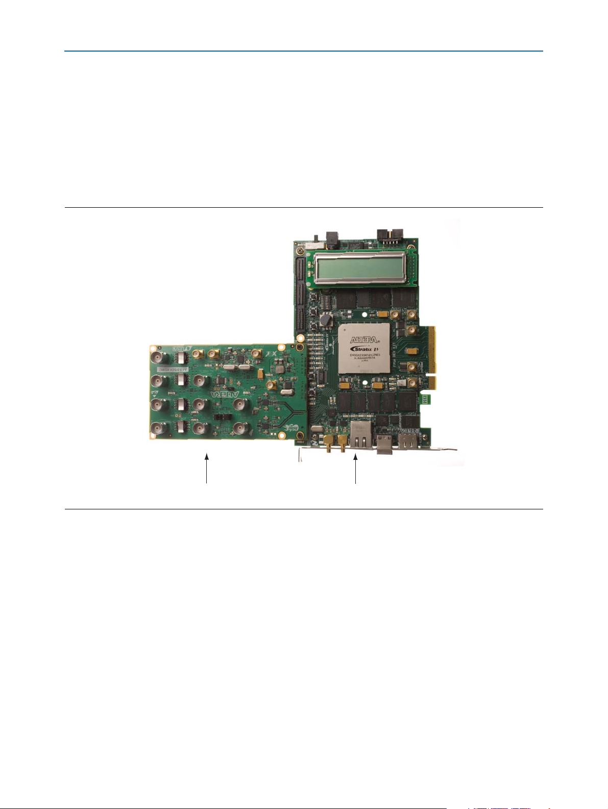
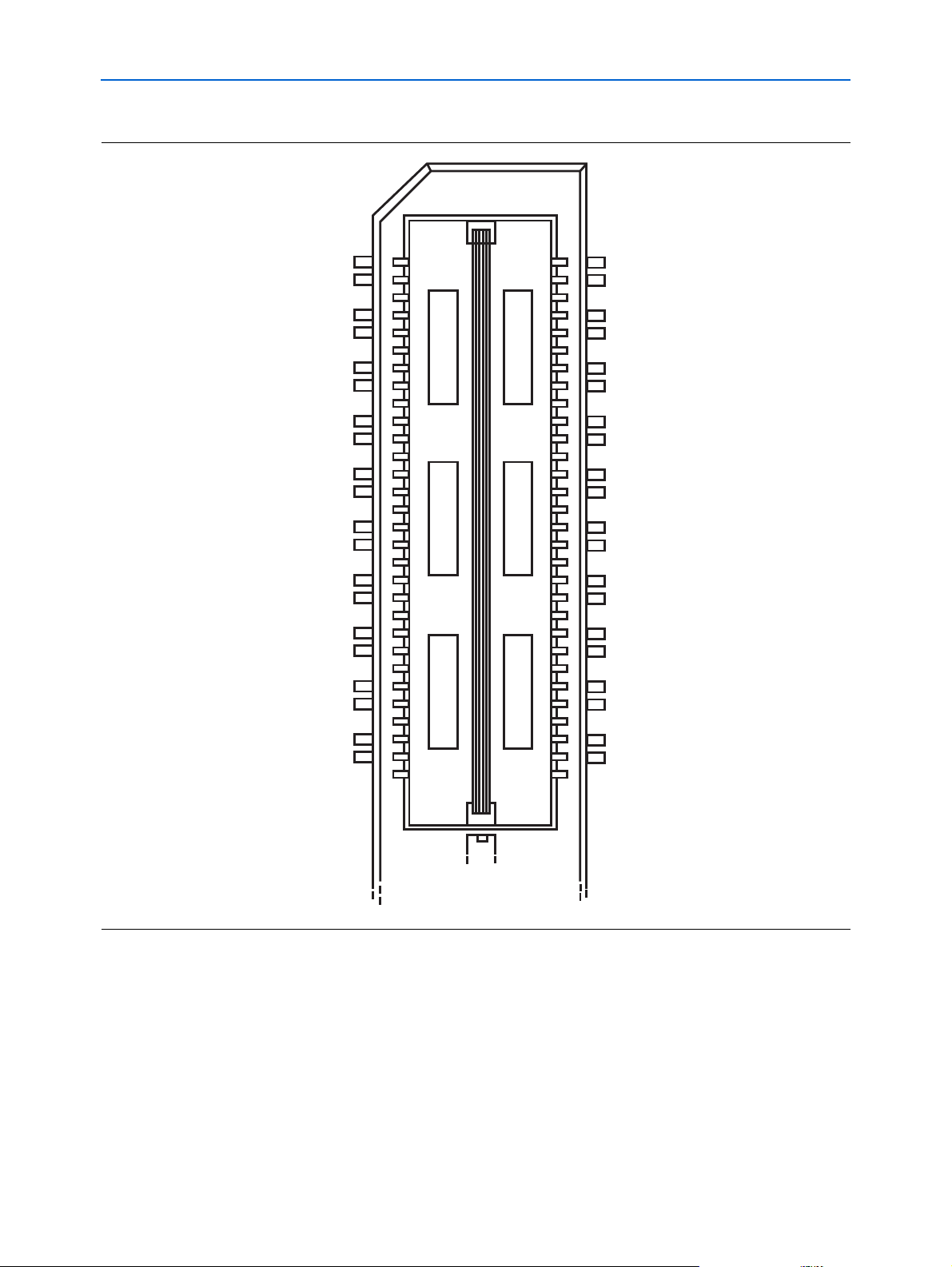
Figure 1–1 shows the SDI HSMC connected to an Altera FPGA development board.
f Refer to the Audio Video Development Kit, Stratix IV GX Edition User Guide for an
example of connecting the SDI HSMC to a host board.
f For detailed information about the board components and interfaces of the Stratix IV
GX FPGA development board, refer to the Stratix IV GX FPGA Development Board
Reference Manual.
Figure 1–1. SDI HSMC Connected to the Stratix IV GX FPGA Development Board
SDI HSMC
Stratix IV GX FPGA Development Board
Development Board Block Diagram
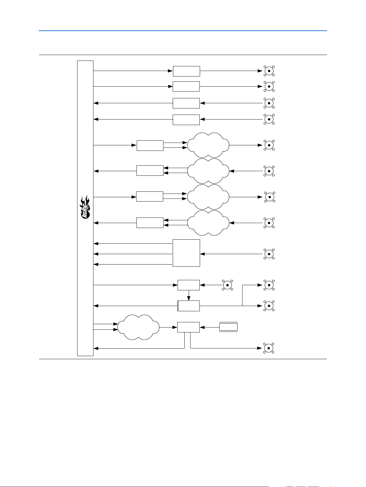
Figure 1–2 shows the functional block diagram of the SDI HSMC. The board has three
distinct areas of interest:
■ SDI
■ AES
■ Clocking
SDI
The SDI includes two high-speed output interfaces from the HSMC to the cable
drivers and to two single-ended 75-Ω BNC output interfaces. There are also two
receive paths which input signals to two 75-Ω BNC connectors to receive equalizers.
The differential signals are then output to the HSMC connector.
SDI HSMC Reference Manual © July 2009 Altera Corporation
Page 7
Chapter 1: Overview 1–3
Board Component Blocks
AES
The AES includes two input and two output interfaces. The interface to the host board
is 2.5-V CMOS signaling. The differential RS 422 line transceivers convert the
single-ended signal to balanced differential outputs which drive the audio isolation
transformers.
Clocking
Clocking is the third area of interest on the board. Clocking for the SDI interfaces is
supported by a dual SDI multi-frequency VCXO femto clock video PLL
(ICS810001-21) from Integrated Device Technology (IDT). The chipset supports
various inputs related to common video signals from the bit rate clocks or horizontal
sync signals. The output of the chipset is fed into a differential clock buffer. The
differential signal is then output to the HSMC connector and SMA connectors. Two
crystal oscillators are used in this chipset — 27 MHz and 27/1.001 MHz (26.973 MHz).
The PLL is used to supply 74.25 MHz or 148.5 MHz reference clocks to the transceiver
on the host board.
Clocking for the AES interfaces is implemented by using the VCXO PLL (ICS275-22),
a pre-programmed IDT part. As applied in the AES interface, a 16.384-MHz crystal is
used in the VCXO section and followed by a PLL to produce the supported
frequencies of 98.304 MHz, 90.3168 MHz, 122.88 MHz, and 112.896 MHz.
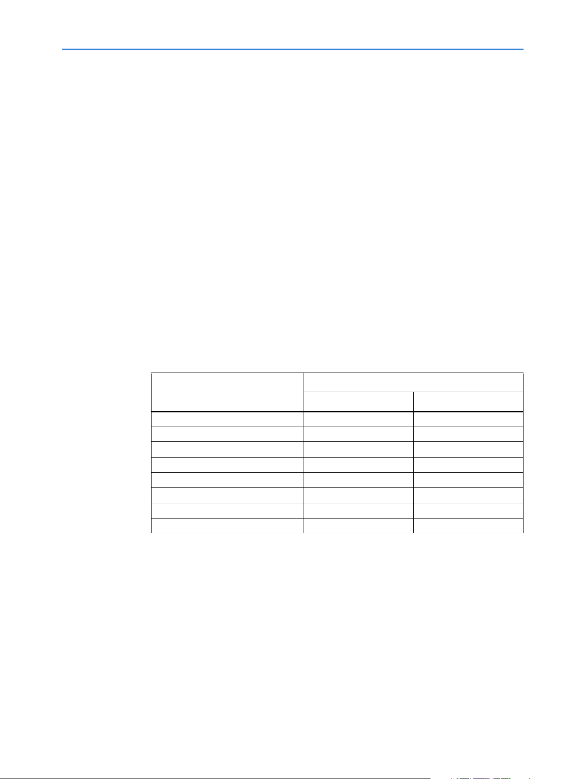
Table 1–1 shows the frequency setup of the VCXO PLL.
Table 1–1. Frequency Setup of the VCXO PLL
Frequency (MHz)
S [2:0]
000 98.304 98.304
001 90.3168 90.3168
010 122.88 122.88
011 112.896 112.896
100 98.304 122.88
101 90.3168 112.896
110 98.304 90.3168
111 122.88 112.896
Pin 5 Pin 6
© July 2009 Altera Corporation SDI HSMC Reference Manual
Page 8
1–4 Chapter 1: Overview
TX 1 DATA
SDI T X 1
EQ 1 SDI RX 1
Video Sync
Separator
Video In
148.5 MHz
HSYNC
VSYNC
Buffer
PLL
PLL Ref / Rec CLK
TX 2 DATA
SDI T X 2
RX 1 DATA
EXT CLK
IN
SDI CLK
OUT (P)
DRV 1
DRV 2
EQ 2 SDI RX 2
RX 2 DATA
AES RX 1
AES TX DATA
AES TX 1
AES RX DAT A
AES Passive
Circuit
AES Passive
Circuit
AES RX 2
AES TX DATA
AES TX 2
AES RX DAT A
AES Passive
Circuit
AES Passive
Circuit
FRAME
SDI CLK
OUT (N)
TX
RX
TX
RX
AES Loop
Filter
VCXO
xtal
AES CLK
SMA
16.384 MHz
AES CLK
down
up
Handling the Board
Figure 1–2. SDI HSMC Block Diagram
Handling the Board
c Static Discharge Precaution: Without proper anti-static handling, the board can be
When handling the board, it is important to observe the following precaution:
damaged. Therefore, use anti-static handling precautions when touching the board.
The SDI HSMC must be stored between –40° C and 100° C. The recommended
operating temperature is between 0° C and 55° C.
SDI HSMC Reference Manual © July 2009 Altera Corporation
Page 9

Introduction
1 A complete set of schematics, physical layout database, and fabrication files for the
f For an example on powering up the board and installing the demonstration software,
2. Board Components
This chapter introduces the important components on the SDI HSMC and provides
their operational and connectivity details.
board is shipped with the board and also resides in the Audio Video Development Kit
Stratix IV GX Edition installation directory.
refer to the Audio Video Development Kit, Stratix IV GX Edition User Guide.
This chapter consists of the following sections:
■ “Board Overview”
■ “Supported Protocols” on page 2–4
■ “Configuration, Status, and Setup Elements” on page 2–5
■ “Clock Circuitry” on page 2–6
■ “General User Input/Output” on page 2–18
■ “Components and Interfaces” on page 2–19
■ “Power Supply” on page 2–24
■ “Restoring Board to Factory Defaults” on page 2–25
Board Overview
This section provides an overview of the SDI HSMC, including an annotated board
image and component descriptions. Figure 2–1 shows the top-view of the SDI HSMC,
including its components and interface locations.
© July 2009 Altera Corporation SDI HSMC Reference Manual
Page 10
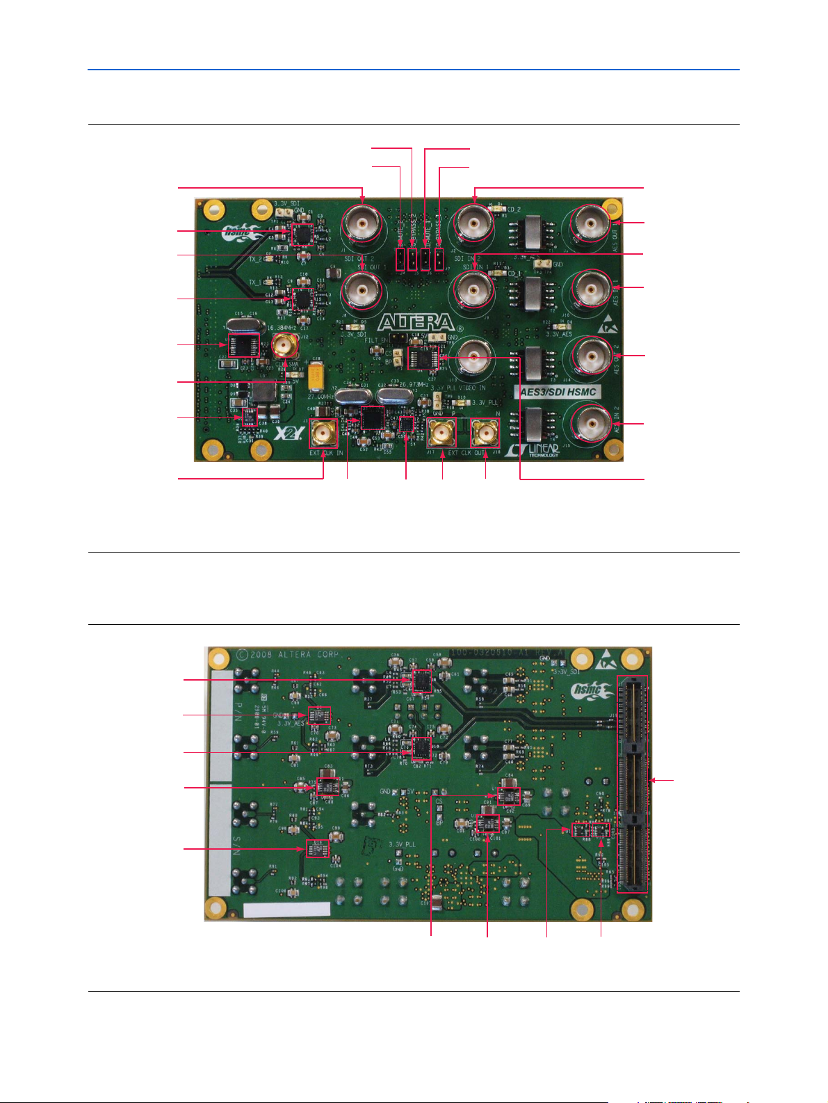
2–2 Chapter 2: Board Components
SMA SDI
Clock Input (J16)
LVPECL
Differential
Clock
Buffer
(J62)
Equalizer Bypass Jumper (J7)
High Frequency
Switching
Regulator (U5)
AES VCXO PLL (U3)
SDI Input
Channel 2 (J2)
Multi-format Video
Sync Separator (U4)
SMA SDI
Clock
Output
(P)
(J17)
SDI
Multi-frequency
VCXO
Femto Clock
Video PLL (U6)
SDI Cable
Tri-speed Driver (U1)
AES Output
Channel 1 (J3)
AES Input
Channel 1 (J10)
AES Output
Channel 2 (J14)
AES Input
Channel 2 (J15)
SDI Output
Channel 2 (J1)
Carrier Detect — Mute Jumper (J4)
SDI Input
Channel 1 (J9)
Carrier Detect — Mute Jumper (J6)
Equalizer Bypass Jumper (J5)
SDI Output
Channel 1 (J8)
SDI Cable
Tri-speed Driver (U2)
SMA SDI
Clock
Output
(N)
(J18)
SMA AES
Clock Output (J12)
Board Overview
Figure 2–1. Top View of the SDI HSMC
Figure 2–2 shows the bottom view of the SDI HSMC.
Figure 2–2. Bottom View of the SDI HSMC (HSMC Connector View)
SDI Cable
Equalizer (U8)
RS422 Transceiver (U9)
Equalizer (U10)
Linear Regulator (U11)
RS422 Transceiver (U16)
SDI Cable
Linear
Regulator
(U12)
Linear
Regulator
(U13)
Single Gate
Tr i-state
Buffer (U14)
Single Gate
Tr i-state
Buffer (U15)
HSMC
Connector (J19)
SDI HSMC Reference Manual © July 2009 Altera Corporation
Page 11
Chapter 2: Board Components 2–3
Board Overview
Table 2–1 describes the components and lists their corresponding board references.
Table 2–1. SDI HSMC Components (Part 1 of 2)
Board Reference Name Description
Devices
U1, U2 SDI cable tri-speed driver Input signal to this driver is from the HSMC high-speed
serializer/deserializer (SERDES) section. The DC blocking caps are in
series with the connector and the integrated circuit (IC).
U3 AES VCXO PLL Programmed VCXO from Integrated Computer Solutions (ICS) to
produce frequencies of 98.304 MHz, 90.3168 MHz, 122.88 MHz, and
112.896 MHz.
U4 Multi-format video sync
separator
U5 High frequency switching
regulator
U6 SDI multi-frequency VCXO
Signals ODDEVEN, VFORMAT, VSYNC, HSYNC from this device are
available to the host board through the HSMC connector.
IC switching power supply configured for a 5 V output. The input
voltage is 12 V from the HSMC connector.
Low jitter femto clock, multi-crystal SDI video PLL.
femto clock video PLL
U7 LVPECL differential clock
buffer
Differential clock signals available at the SMA outputs and HSMC
connector.
U8, U10 SDI cable equalizer Equalizes data transmitted over the cable.
U9, U16 RS422 transceiver Used as a differential line driver and receiver for the AES interface.
U11, U12, U13 Linear regulator Regulator with an input of 5 V and output of 3.3 V.
U14, U15 Single gate tri-state buffer For AES VCXO control.
SDI Inputs/Outputs
J1 SDI output channel 2 Output is through a BNC connector driven from the SDI cable driver.
J8 SDI output channel 1 Output is through a BNC connector driven from the SDI cable driver.
J2 SDI input channel 2 The signal from this channel is input to a cable equalizer. This equalizer
can be bypassed.
J9 SDI input channel 1 The signal from this channel is input to a cable equalizer. This equalizer
can be bypassed.
AES Inputs/Outputs
J3 AES output channel 1 Transformer-coupled output with 75-Ω driver impedance.
J10 AES input channel 1 A 75-Ω transformer coupled with AES input channel.
J14 AES output channel 2 Transformer-coupled output with 75-Ω driver impedance.
J15 AES input channel 2 A 75-Ω transformer coupled with AES input channel.
Clocks
J16 SMA SDI clock input This signal is input to the SDI clock PLL (CMOS). There is a 49.9-Ω
termination to ground at the pin.
J17 SMA SDI clock output (P) An ECL compatible output. The ECL bias includes a 130-Ω pull-up to
3.3 V and a 82-Ω pull-down to ground.
J18 SMA SDI clock output (N) An ECL compatible output. The ECL bias includes a 130-Ω pull-up to
3.3 V and a 82-Ω pull-down to ground.
J12 SMA AES clock output This signal is output to the SMA AES clock (CMOS) and has a 33-Ω
series termination resistor.
© July 2009 Altera Corporation SDI HSMC Reference Manual
Page 12
2–4 Chapter 2: Board Components
Supported Protocols
Table 2–1. SDI HSMC Components (Part 2 of 2)
Board Reference Name Description
General User Input/Output
J7 SDI input 1 equalizer bypass
jumper
J5 SDI input 2 equalizer bypass
jumper
J6 SDI input 1 auto-mute enable
jumper
J4 SDI input 2 auto-mute enable
jumper
Installing a jumper on J7 enables the LMH0344 device's equalization
and DC restoration features for channel 1. Removing a jumper from J7
bypasses the equalizer (default). This can also be controlled by driving
EQ_BYPASS1 low from the HSMC host board through connector J19
pin 77. Remove the jumper when controlling from the HSMC host
board's FPGA.
Installing a jumper on J5 enables the LMH0344 device's equalization
and DC restoration features for channel 2. Removing a jumper from J5
bypasses the equalizer (default). This can also be controlled by driving
EQ_BYPASS2 low from the HSMC host board through connector J19
pin 79. Remove the jumper when controlling from the HSMC host
board's FPGA.
Installing a jumper on J6 enables the LMH0344 device's carrier detect
function to auto-mute its own output when no input signal is detected
from J9 for channel 1. Removing a jumper from J6 causes the mute
function to be enabled. Altera recommends to leave this jumper
installed.
Installing a jumper on J4 enables the LMH0344 device's carrier detect
function to auto-mute its own output when no input signal is detected
from J2 for channel 2. Removing a jumper from J4 may cause the mute
function to be enabled. Altera recommends to leave this jumper
installed.
Components and Interfaces
J19 HSMC connector SDI HSMC’s main interface to the host board. The host must support
3-Gbps interfacing on transceiver channels 0 and 1 (first 2 channels)
which are located at pins 25 – 32. The control, clock, and AES signals
are located in the general CMOS signal area. The AES clock is
single-ended while the SDI clock is differential.
Power
J19 HSMC 12-V input 12-V input from the HSMC connector is utilized for board power
generation. Power of 5 V is produced by a low noise high frequency
switcher. Three linear regulators are used to produce 3.3 V from the 5-V
power rail.
Supported Protocols
Table 2–2 lists the SDI video standards supported by the SDI HSMC.
Table 2–2. SDI supported protocols
Rate Video Standard
Standard Definition (SD) NTSC, PAL
High Definition (HD) 720p50, 720p59, 720p60, 1080s23.98, 1080s24, 1080i50, 1080i60, 1080p29.97, 1080p30
Third-Generation (3G) 1080p50, 1080p59.9, 1080p60
SDI HSMC Reference Manual © July 2009 Altera Corporation
Page 13
Chapter 2: Board Components 2–5
Configuration, Status, and Setup Elements
Although there is only one clock generator PLL on the SDI HSMC, the board supports
two asynchronous clock systems when the host board supports two reference clock
input signals. You can use either a separate reference clock or an external reference as
input to the host board.
Table 2–3 describes the features of the oversampling rate and associated clock
frequency for each supported audio sample rate.
Table 2–3. AES3 Supported Bit Rates
Bit Rate Clock (MHz)
Audio Sample Rate (kHz)
24.0 3.0720 32 98.304
32 4.0960 24 98.304
44.1 5.6448 16 90.3168
48 6.1440 16 98.304
88.2 11.2896 8 90.3168
96 12.2880 8 98.304
176.4 22.5792 4 90.3168
192 24.5760 4 98.304
24.0 3.0720 40 122.8800
32 4.0960 30 122.8800
44.1 5.6448 20 112.8960
48 6.1440 20 122.8800
88.2 11.2896 10 112.8960
96 12.2880 10 122.8800
176.4 22.5792 5 112.8960
192 24.5760 5 122.8800
(32 x 2 x 2) Oversampling Rate VCXO Frequency
Configuration, Status, and Setup Elements
This section describes board configuration, status, and setup.
Configuration
The standard jumper configuration has J4 (CD_MUTE2) and J6 (CD_MUTE1) installed.
Jumpers J5 (EQ_BYPASS2) and J7 (EQ_BYPASS1) can be driven from the host board.
These signals bypass the SDI cable equalizer when logic 1 is driven.
Status Elements
The development board includes status LEDs. This section describes the status
elements.
Table 2–4 lists the LED board references and functional descriptions.
© July 2009 Altera Corporation SDI HSMC Reference Manual
Page 14

2–6 Chapter 2: Board Components
Clock Circuitry
Table 2–4. LED Board References and Functional Descriptions
Board Reference Schematic Signal Name Description
D2 — Green LED. Illuminates when carrier is detected in channel 2.
D4 — Green LED. Illuminates when carrier is detected in channel 1.
D7 — Green LED. Illuminates when 3.3-V SDI power is active.
D8 — Green LED. Illuminates when 3.3-V AES power is active.
D9 — Green LED. Illuminates when 5-V power is active.
D12 — Green LED. Illuminates when 3.3-V PLL power is active.
D1 SDI_LED_RX_G2,
SDI_LED_RX_R2
Bi-color LED. Illuminates in:
■ Green when SDI_LED_RX_G2 signal is driven low.
■ Red when SDI_LED_RX_R2 signal is driven low.
■ Orange when both SDI_LED_RX_G2 and SDI_LED_RX_R signals are
driven low.
D3 SDI_LED_TX_G2,
SDI_LED_TX_R2
Bi-color LED. Illuminates in:
■ Green when SDI_LED_TX_G2 signal is driven low.
■ Red when SDI_LED_TX_R2 signal is driven low.
■ Orange when both SDI_LED_TX_G2 and SDI_LED_TX_R2 signals
are driven low.
D5 SDI_LED_TX_G1,
SDI_LED_TX_R1
Bi-color LED. Illuminates in:
■ Green when SDI_LED_TX_G1 signal is driven low.
■ Red when SDI_LED_TX_R1 signal is driven low.
■ Orange when both SDI_LED_TX_G1 and SDI_LED_TX_R1 signals
are driven low.
D6 SDI_LED_RX_G1,
SDI_LED_RX_R1
Bi-color LED. Illuminates in:
■ Green when SDI_LED_RX_G1 signal is driven low.
■ Red when SDI_LED_RX_R1 signal is driven low.
■ Orange when both SDI_LED_RX_G1 and SDI_LED_RX_R1 signals
are driven low.
Clock Circuitry
This section describes the board's clock inputs and outputs.
SDI Clock
You can generate the reference clocks from the host board, external video sources, and
external SDI sources. The output of the clock generator should be set up to produce a
frequency of 148.5 MHz or 148.5 MHz/1.001 (148.35 MHz). Outputs from the
differential buffer are available at SMA outputs and also at the HSMC connector. The
SMA outputs are provided for use as a low-jitter signal directed into a SERDES
reference clock input on the host board.
Figure 2–3 shows the SDI HSMC clocking diagram.
SDI HSMC Reference Manual © July 2009 Altera Corporation
Page 15

Chapter 2: Board Components 2–7
Cl ock
Generator
Video Sync
Separator
Video In
PLL Settings
SDI CLK
HSYNC
VSYNC
LF
EXT CLK IN
EXTCLK_OUT (P)
SDI HSMC CLK
Differential
Buffer
EXTCLK_OUT (N)
SDI CLK (N)
SDI CLK (P)
27.000 MHz
26.973 MHz
Clock Circuitry
Figure 2–3. SDI HSMC Clocking Diagram
the SDI reference clocks. The board inputs two crystals to the clock generator, a
27 MHz and 26.973027 MHz. The two frequencies allow low-jitter operation for US
and European SDI standard rates. The HSMC signal SDI_XTAL_SEL determines
which crystal is locked by the internal VCXO.
Clock inputs to the SDI PLL come from the HSMC host or through an SMA input.
Both inputs are end-terminated at 50 Ω to ground. The HSMC signal SDI_CLK_SEL
The SDI multi-frequency VCXO femto clock video PLL (ICS810001-21) is utilized for
f For more information on the SDI multi-frequency VCXO femto clock video PLL, refer
© July 2009 Altera Corporation SDI HSMC Reference Manual
determines which input is active.
to the data sheet provided by IDT.
Figure 2–4 shows the SDI multi-frequency VCXO femto clock video PLL block
diagram.
Page 16

2–8 Chapter 2: Board Components
Output
Divider
00 = 4
01 = 8
10 = 12
11 = 18
SDI CL K
VCXO Input
Pre-divider
(P Value from
Table 2-6)
2
2
4
VCXO Feedback Divider
(M Value from Table)
0
1
Femto Clock
Frequency Multiplier
0 = x22
1 = x24
VCXO PLL
Divider
Look-up Table
VCXO
0
1
01
10
11
00
01
10
11
0
1
+
–
CLK0
CLK1
CLK_SEL
V3:V0
MR
Master Reset
MF
N1:N0
nBP1:nBP0
Phase
Detector
Charge
Pump
ISET
VCXO Jitter Attenuation PLL
LF0
Loop
Filter
LF1
XTAL_IN0
XTAL_OUT0
XTAL_IN1
XTAL_OUT1
XTAL_SEL
Clock Circuitry
Figure 2–4. SDI Multi-Frequency VCXO Femto Clock Video PLL Block Diagram
The clock control signals SDI_CLK_V[3:0] control the input divider for the first
translation stage of the SDI multi-frequency VCXO femto clock video PLL. Tab le 2–5
shows which frequency inputs lock to either 27 MHz or 26.973027 MHz crystals.
Various "P" and "M" preset divider options can be selected by adjusting the values to
produce a frequency of 27 MHz or the alternate frequency out of the VCXO. The "P"
divider divides the input frequency to the comparison frequency used by the phase
detector. The "M" divider divides the output frequency of the VCXO to the
comparison frequency used by the phase detector. After the VCXO is locked to
27 MHz (or alternate), the signal is then multiplied up to the output frequency by the
femto clock PLL (refer to Tabl e 2 –6). The output frequency can be 148.5 MHz,
74.25 MHz, 54 MHz, or 36 MHz. The output frequency is set to 148.5 MHz for the
SDI HSMC Reference Manual © July 2009 Altera Corporation
Altera reference design and most applications.
Table 2–5 lists the first frequency translation stage of the SDI multi-frequency VCXO
femto clock video PLL.
Page 17

Chapter 2: Board Components 2–9
Clock Circuitry
Table 2–5. First Frequency Translation Stage of the SDI Multi-Frequency VCXO Femto Clock Video PLL
VCXO PLL Divider Look-Up Table Video Clock Application Alternate Video Clock Application
V3:V0 Pins P Value M Value Input VCXO Input VCXO
0000 1000 1000 27 MHz 27 MHz 26.973 MHz 26.973 MHz
0010 1001 1000 27 MHz 26.973 MHz — —
0010 11000 4004 74.175 MHz 27 MHz — —
0011 11011 4000 74.25 MHz 26.973 MHz — —
0100 11000 4000 74.25 MHz 27 MHz — —
0101 4004 4004 27 MHz 27 MHz 26.973 MHz 26.973 MHz
0110 4004 4000 27 MHz 26.973 MHz — —
0111 1000 1001 26.973 MHz 27 MHz — —
1000 250 91 74.175 MHz 27 MHz — —
1001 253 92 74.25 MHz 27 MHz — —
1010 92 92 27 MHz 27 MHz 26.973 MHz 26.973 MHz
1011 1 600 45 kHz
(720P/60 hsync)
1100 1 800 33.75 kHz
(1080l/60 hsync)
1101 1 1728 15.625 kHz
27 MHz 44.955 kHz
26.973 MHz
(720P/59.94)
27 MHz 33.716 kHz
26.973 MHz
(1080l/59.94)
27 MHz — —
(PAL hsync)
1110 1 1716 15.734 kHz
27 MHz — —
(NTSC hsync)
1111 1 960 28.125 kHz
27 MHz — —
(1080l/50 hsync)
Table 2–6 lists the second frequency translation stage of the SDI multi-frequency
VCXO femto clock video PLL.
Table 2–6. Second Frequency Translation Stage of the SDI Multi-Frequency VCXO Femto Clock Video PLL
Femto Clock Look-Up Table Video Clock Application Alternate Video Clock Application
MF, N1:N0 Pins FB Div Out Div VCXO Q VCXO Q
0,00 22 4 27 MHz 148.5 MHz 26.973 MHz 148.35 MHz
0,01 22 8 27 MHz 74.25 MHz 26.973 MHz 74.175 MHz
0,102212————
0,112218————
1,00244————
1,01248————
1,10 24 12 27 MHz 54 MHz — —
1,11 24 18 27 MHz 36 MHz — —
Table 2–7 shows the bypass function of the SDI multi-frequency VCXO femto clock
video PLL.
© July 2009 Altera Corporation SDI HSMC Reference Manual
Page 18
2–10 Chapter 2: Board Components
IN
V
T
/IN
Q0
/Q0
Q1
/Q1
50 Ω
50 Ω
V
REF
– AC
Clock Circuitry
Table 2–7. Bypass Function Table
Inputs
Operation
nBP1 nBP0
0 0 Bypass frequency translator PLL and output divider.
0 1 Test mode: Bypass VCXO jitter attenuation PLL and frequency translator PLL.
1 0 LC mode: Bypass VCXO jitter attenuation PLL.
1 1 PLL mode: Active.
1 The nBP signals shown in Table 2–7 are mainly used for testing. For normal operation,
the nBP signals are both driven to logic 1.
The output of the clock generator is single-ended. To avoid common mode noise that
might be present in the signaling path from the clock generator to the HSMC host
device, a differential LVPECL clock buffer is employed to convert the reference clock
to differential signal and drive the signal to the host device. The LVPECL differential
clock buffer (SY58012) has the advantages of a fast edge rate and low jitter.
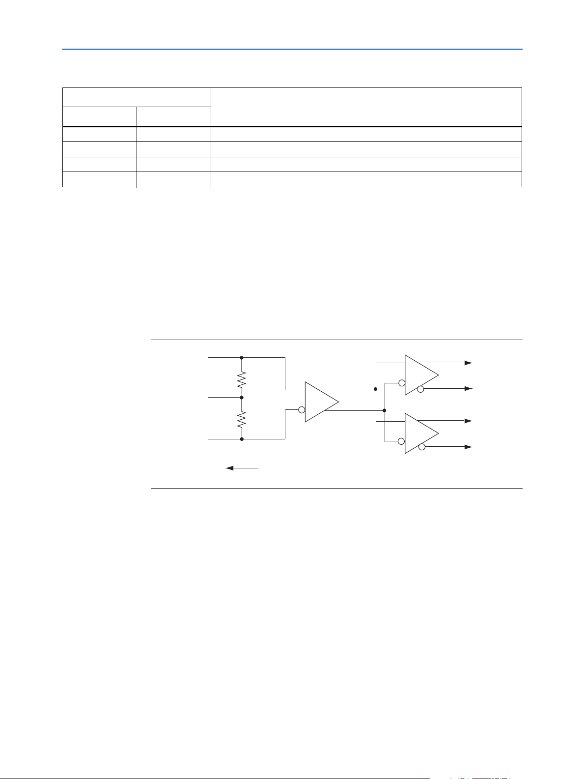
Figure 2–5 shows a simplified block diagram of the LVPECL differential clock buffer.
Figure 2–5. LVPECL Differential Clock Buffer
The differential outputs at Q0 are connected to the HSMC connector and drive the
clock signal to the host device. The outputs at Q1 have output bias resistors and are
connected to two 50-Ω SMA connectors. These outputs serve as a low jitter source to
sync up other system devices and to trigger on test equipment or alternate reference
clock source to the host board.
Host Board Reference Clock
You can select one of the several reference clock frequencies to input as a reference to
the SDI multi-frequency VCXO femto clock video PLL. For example, if the host board
has a 100-MHz oscillator, you can divide the frequency by 6,400 to 15.625 kHz and
drive that frequency to the clock generator to be multiplied to 148.5 MHz. Altera
recommends locking the VCXO PLL to a stable oscillator which is located on the host
SDI HSMC Reference Manual © July 2009 Altera Corporation
board when the daughtercard is sourcing data or when the VCXO PLL is not locked
onto a received signal or reference. This locking prevents wandering or frequency
hunting.
Page 19

Chapter 2: Board Components 2–11
Clock Circuitry
Loop Back Reference Clock From SDI Input
When an RX channel is locked onto the input data stream, the recovered clock
represents the actual bit rate of that stream. This recovered clock is often 74.25 MHz
and can be buffered from the host board and driven out through the HSMC interface
to the clock generator on the SDI HSMC. The clock output from the host is cleaned
(jitter), multiplied to 148.5 MHz, and driven back to the host board to be used as the
SERDES reference clock. Using this technique maintains the flow through timing.
Studio Reference Timing
If a studio clock source (a 27-MHz source) is available, the source can be connected to
the EXT CLK IN SMA port on the daughtercard.
Studio Reference Video Timing
A video synchronization separator is provided to synchronize the SDI video output
streams to analog video. The horizontal and vertical syncs are driven to the host board
and can be driven back to the video clock generator chip to produce a 148.5-MHz
SERDES reference.
Table 2–8 shows the board's clock distribution.
AES3 Clock
Table 2–8. SDI HSMC Clock Distribution
Frequency Schematic Signal Name Signal Originates From Signal Propagates To
148.5 MHz SDI_CLK_P U7.12 J19.156 (HSMC)
SDI_CLK_N U7.11 J19.168 (HSMC)
98.304 MHz AES_CLK, U3.5 J19.96 (HSMC)
AES_CLK_SMA U3.6 J12 (SMA)
AES3 clocking uses a semi-custom clock device from IDT (ICS275-22). The device
comes pre-programmed to produce 93.304 MHz, 90.3168 MHz (4× oversampling),
122.88 MHz, and 112.896 MHz (5× oversampling) from a 16.384-MHz crystal. Most
combinations are available at outputs CLK1 and CLK2. Output CLK1 is connected to
the HSMC connector and drives a signal to the host device. Output CLK2 is connected
to an output SMA connector. You can use this output for a reference, to trigger test
equipment, or to sync a signal to other devices in the AES3 system.
The base part (ICS275) is a VCXO that can have various combinations of input,
output, and feedback dividers to produce variations of the crystal frequency. The
control voltage input of the device is controlled by a passive network of resistors and
capacitors that are connected to tri-state buffers, one driven high and the other driven
low when in the active state (non-tri-stated). The single gate devices are powered by
3.3 V to allow full swing of the control voltage (V
, AES_CLK_V) because the ICS275
IN
is also powered by 3.3 V. The tri-state-enabled pins are controlled by the host device
connected to the HSMC. These pins should not be allowed to float.
To use the ICS275 as a normal oscillator and not as a VCXO, drive signals
AES_VCXO_UP and AES_VCXO_DN both to logic 1. Both output signals are enabled
and the resulting voltage output after the resistor or capacitor network is a
mid-voltage driven to the V
© July 2009 Altera Corporation SDI HSMC Reference Manual
of the ICS275 device.
IN
Page 20

2–12 Chapter 2: Board Components
16.384 MHz
Crystal Input
Voltage-controlled
Crystal Oscillator
2
3
PLL1
PLL2
PLL3
One-time-
programmable
ROM
with PLL
Values
Divide
Logic
and
Output
Enable
Control
CLK1
CLK2
CLK3
CLK4
PDTS
GND
External Capacitors
S2:S0
VDD
X1
X2
V
IN
3
Clock Circuitry
To use the ICS275 as a VCXO in a PLL application, connect the phase detector to the
AES3 up and down control signals.
Figure 2–6 shows the AES VCXO PLL block diagram.
Figure 2–6. AES VCXO PLL Block Diagram
Table 2–9 shows the audio rate and clock frequencies supported by the SDI HSMC.
Table 2–9. Audio Sample Rate versus Clock Frequency (Part 1 of 2)
Audio Sample Rate (kHz) Bit Rate Clock (MHz) Oversampling Rate VCXO Frequency
24.00 3.0720 32 98.3040
32.00 4.0960 24 98.3040
44.10 5.6448 16 90.3168
48.00 6.1440 16 98.3040
88.20 11.2896 8 90.3168
96.00 12.2880 8 98.3040
176.4 22.5792 4 90.3168
192 24.5760 4 98.3040
24.00 3.0720 40 122.8800
32.00 4.0960 30 122.8800
44.10 5.6448 20 112.8960
48.00 6.1440 20 122.8800
88.20 11.2896 10 112.8960
96.00 12.2880 10 122.8800
SDI HSMC Reference Manual © July 2009 Altera Corporation
Page 21

Chapter 2: Board Components 2–13
Clock Circuitry
Table 2–9. Audio Sample Rate versus Clock Frequency (Part 2 of 2)
Audio Sample Rate (kHz) Bit Rate Clock (MHz) Oversampling Rate VCXO Frequency
176.4 22.5792 5 112.8960
192 24.5760 5 122.8800
Table 2–10 defines the frequency output with respect to the three 1-bit control signals,
S[2:0]. Outputs from CLK3 and CLK4 are not used in the VCXO PLL. The
frequencies programmed into the VCXO PLL support 4x and 5x over-sampling of the
most popular audio sample rates.
Table 2–10. VCXO PLL Frequency Output
S2 S1 S0 CLK1 (MHz) CLK2 (MHz) CLK3 CLK4
0 0 0 98.304 98.304 OFF OFF
0 0 1 90.3168 90.3168 OFF OFF
0 1 0 122.88 122.88 OFF OFF
0 1 1 112.896 112.896 OFF OFF
1 0 0 98.304 122.88 OFF OFF
1 0 1 90.3168 112.896 OFF OFF
1 1 0 98.304 90.3168 OFF OFF
1 1 1 122.88 112.896 OFF OFF
© July 2009 Altera Corporation SDI HSMC Reference Manual
Page 22

2–14 Chapter 2: Board Components
Audio/Video Input and Output
Audio/Video Input and Output
This section describes the I/O channels of the SDI HSMC which includes:
■ SDI RX Channels
■ SDI TX Channels
■ AES3 RX Channels
■ AES3 TX Channels
SDI RX Channels
The SDI RX channel consists of an SDI cable equalizer (LMH0344) with bypass, an
input matching network, an input vertical mount with a 4-GHz BNC connector, a
bypass control signal, DC blocking caps on the input and output, and a carrier detect
LED.
f For the RX channel circuit diagram, refer to the schematic page entitled RX1/2
Equalizer on page 3 and 4 of the Altera schematic 150-0320610-B1. In Altera
development kits that contain the SDI HSMC, this schematic resides in the
<install dir>\board_design_files directory.
Jumpers J4 and J6 short the CD_MUTE signal and connect carrier detect to the mute
input of the SDI receiver equalizer. In normal operation, these two jumpers are
installed. Jumpers J5 and J7 short the EQ_BYPASS signal to ground, thus not
bypassing the input cable equalizer portion of the SDI cable equalizer. A 10-kΩ
resistor sets the signal to 3.3 V on both channels. This signal can also be controlled by
the host through the HSMC connector (pins 77 and 79 of the HSMC connector).
Jumpers J5 and J7 are normally not installed. If the HSMC host does not drive this
signal, then the SDI cable equalizer is in bypass mode.
The RX channel receives 270 Mbps, 1.485 Gbps, and 2.970 Gbps SDI signals through a
single-ended 75-Ω BNC connector. The signals traverse an impedance-matching
network provided by the manufacturer. The input signal is terminated to ground with
a 75-Ω external resistor and is input into the SDI cable equalizer via a 1-µF DC
blocking capacitor. The opposite leg of the SDI cable equalizer's differential input pin
is terminated in the same way as the input signal and serves to correctly balance the
input bias currents internal to the equalizer. The equalizer then equalizes the signal
and outputs a 100-Ω differential signal to the SERDES receiver located on the host
HSMC device. The differential output of the SDI cable equalizer passes through 1-µF
DC blocking capacitors.
There are bi-colored LEDs next to the RX BNC connectors. The LEDs are connected to
3.3V_SDI power rail through a 75-Ω resistor and are controlled by signals
SDI_LED_RX_G and SDI_LED_RX_R. These signals are connected to the HSMC
connector and driven from the host board. The LEDs illuminate when a zero is driven
on the LED control signals. The voltage drop across the LED is approximately 2.1 V. A
zero voltage at the HSMC connector on the LED control signals causes a drop of
16 mA. Knowing this information, you can program the four states of the LEDs to
indicate the RX bit rate.
Figure 2–7 shows the SDI RX channel block diagram.
SDI HSMC Reference Manual © July 2009 Altera Corporation
Page 23

Chapter 2: Board Components 2–15
bypass
SDI Cable
Equalizer
LR
Network + Term
SDI RX
Carrier Detect
DC Block
DC Block
Audio/Video Input and Output
Figure 2–7. SDI RX Channel Block Diagram
SDI TX Channels
f For the TX channel circuit diagram, refer to the schematic page entitled SDI Cable
The SDI TX channel consists of a SDI cable tri-speed driver (LMH0302) with slew rate
control, an output impedance matching network, an output vertical mount with a
4-GHz BNC connector, an SDI rate select control signal, DC blocking caps on the input
and output, and a red/green LED.
Driver on page 5 of Altera schematic 150-0320610-B1. In Altera development kits that
contain the SDI HSMC, this schematic resides in the <install dir>\board_design_files
directory.
The SDI_RATE_SEL signal is driven from the host device through the HSMC
connector pins 71 and 73. These pins should not be allowed to float. A logic 1 reduces
the slew rate to match the SD-SDI signaling requirements while a logic 0 increases the
output slew rate of the SDI cable driver and is used when transmitting 1.485 Gbps rate
(HD) and 2.970 Gbps rate (3G).
© July 2009 Altera Corporation SDI HSMC Reference Manual
Page 24

2–16 Chapter 2: Board Components
Audio/Video Input and Output
The SDI TX channel transmit 270 Mbps, 1.485 Gbps and 2.970 Gbps rates using a 75-Ω
coaxial cable. The SDI signals traverses an impedance matching network provided by
the manufacturer and then goes through a DC blocking capacitor before being sent to
the BNC connector. The output signal is back-terminated to 3.3 V externally with 75-Ω
resistors. The output DC blocking capacitors consist of 4.7-µF capacitors. The opposite
leg of the SDI cable driver’s differential output pin is terminated in the same way as
the output signal and serves to correctly balance the output currents internal to the
device.
The output of the TX pins on the HSMC host boards should not be installed with DC
blocking capacitors. If DC blocking capacitors are installed, remove the capacitors and
install 0-Ω resistors of the same foot print size (0402). The input of the SDI cable driver
is differentially terminated with a 100-Ω resistor and has 4.7-µF DC blocking
capacitors.
There are bi-colored LEDs next to the TX SDI cable driver. The LEDs are connected to
the 3.3 V_SDI power rail through a 75-Ω resistor and are controlled by signals
SDI_LED_TX_G and SDI_LED_TX_R. These signals are connected to the HSMC
connector and driven from the host board. The LEDs illuminates when a zero is
driven on the LED control signals. The voltage drop across the LED is approximately
2.1 V. A zero voltage at the HSMC connector on the LED control signals would cause a
drop of 16 mA.
Figure 2–8 shows the SDI TX channel block diagram.
Figure 2–8. SDI TX Channel Block Diagram
DC Block
Diff Term
Rate
Sel
SDI Cable
Tri-speed
Driver
LR
Network + Term
DC Block
SDI T X
SDI HSMC Reference Manual © July 2009 Altera Corporation
Page 25

Chapter 2: Board Components 2–17
Audio/Video Input and Output
AES3 RX Channels
The AES3 RX channel delivers a 75-Ω load termination with a return loss of 25 dB or
more. Figure 2–9 shows a simplified block diagram of the AES3 RX channel. The
signal is input through a 75-Ω BNC and terminated with a 75-Ω resistor to ground.
The unbalanced signal is then balanced through an isolation transformer. The
differential signal output from the transformer is biased and input to a RS422
transceiver. The output of the RS422 transceiver is a single-ended LVCMOS signal
which is driven to the host board through the HSMC connector.
Figure 2–9 shows the AES3 RX channel block diagram.
Figure 2–9. AES3 RX Channel Block Diagram
AES3 RX
Resi stor
Termination
AES3 TX Channels
Isolation
Transformer
Bias
Resistor
RS422
Driver
The AES3 TX channel is designed to have a balanced signal driver to the isolation
transformer. The output of the RS422 transceiver has an RX network to limit the
output slew rate, thus limiting the bandwidth of AES3 output. The AES3 channel is
designed to support 192-kHz to 24-kHz sample rates. The output is unbalanced with a
source impedance of 75 Ω and a return loss of 25 dB or more. The peak-to-peak output
voltage is 1.0 V centered around the ground of the transmitter.
Figure 2–10 shows the AES3 TX channel block diagram.
© July 2009 Altera Corporation SDI HSMC Reference Manual
Page 26

2–18 Chapter 2: Board Components
General User Input/Output
Figure 2–10. AES3 TX Channel Block Diagram
RS422
Driver
RC
Network
Isolation
Transformer
General User Input/Output
This section describes the user I/O interface to the board.
Jumpers
The board jumper switches are CD_MUTE channels 1 and 2 and EQ_BYPASS channels 1
and 2. In the factory default board configuration, jumpers are installed on the
CD_MUTE jumper switches (J4 and J6) and not installed on the EQ_BYPASS jumper
switches (J5 and J7). When jumpers are not installed on J5 and J7, the EQ_BYPASS
signal can be controlled from the host device.
Tabl e 2– 11 lists the jumper descriptions and schematic signal names.
Resi stor
Termination
AES3 TX
SDI HSMC Reference Manual © July 2009 Altera Corporation
Page 27

Chapter 2: Board Components 2–19
Components and Interfaces
Table 2–11. Jumper Descriptions and Schematic Signal Names
Board
Reference
J4 CD_MUTE2 Carrier detect jumper switch which connects to RX channel 2
J5 EQ_BYPASS2 Equalizer bypass for RX channel 2. The equalizer can be bypassed
J6 CD_MUTE1 Carrier detect jumper switch which connects to RX channel 1
J7 EQ_BYPASS1 Equalizer bypass for RX channel 1. The equalizer can be bypassed
Schematic
Signal Name Description I/O Standard
(CD_MUTE2) on U8. This jumper is normally installed.
manually when EQ_BYPASS2 signal is tri-stated. This jumper is
normally not installed and the switch is controlled by asserting the
EQ_BYPASS2 signal. A high signal bypasses the SDI receiver equalizer.
(CD_MUTE1) on U10. This jumper is normally installed.
manually when EQ_BYPASS1 signal is tri-stated. This jumper is
normally not installed and the switch is controlled by asserting the
EQ_BYPASS1 signal. A high signal bypasses the SDI receiver equalizer.
Table 2–12 lists the jumper component reference and the manufacturing information.
Table 2–12. Jumper Component Reference and Manufacturing Information
Manufacturer
Board Reference Device Description Manufacturer
J4, J6 Jumper Shunt AMP/Tyco 881545-2 www.tycoelectronics.com
Part Number Manufacturer Website
Signal short
CMOS
Signal short
CMOS
Components and Interfaces
This section describes the SDI HSMC interface.
The SDI HSMC contains an Altera standard HSMC connector to connect to a host
board. All the other connector interfaces on the SDI HSMC are connected to the
HSMC connector.
Figure 2–11, Figure 2–12, and Figure 2–13 show the pin-outs of the HSMC connector
for banks 1, 2, and 3, respectively.
© July 2009 Altera Corporation SDI HSMC Reference Manual
Page 28
2–20 Chapter 2: Board Components
Components and Interfaces
Figure 2–11. HSMC Connector Bank 1 Pin-Outs
NC 2
NC
NC
NC
NC
NC
NC
NC
NC
NC
NC
NC
SDI_EQOUT_P2
SDI_EQOUT_N2
SDI_EQOUT_P1
SDI_EQOUT_N1
NC
NC
10
12
14
16
18
20
22
24
26
28
30
32
34
36
1
NC
4
6
8
3
NC
NC
5
NC
7
9
NC
11
NC
13
NC
15
NC
17
NC
19
NC
NC
21
23
NC
SDI_TX_P2
25
27
SDI_TX_N2
SDI_TX_P1
29
31
SDI_TX_N1
33
NC
35
NC
JTAG_TDO_TDI
SDI HSMC Reference Manual © July 2009 Altera Corporation
NC
38
40
JTAG_TDO_TDI
37
NC
39
Page 29

Chapter 2: Board Components 2–21
Components and Interfaces
Figure 2–12. HSMC Connector Bank 2 Pin-Outs
SDI_LED_TX_R1
NC
NC
12 V
NC
NC
12 V
NC
NC
12 V
NC
NC
12 V
NC
NC
12 V
NC
NC
12 V
NC
NC
12 V
NC
NC
12 V
NC
NC
12 V
AES_CLK
NC
12 V
42
44
46
48
50
52
54
56
58
60
62
64
66
68
70
72
74
76
78
80
82
84
86
88
90
92
94
96
98
100
41
SDI_LED_TX_R2
43
3.3 V
45
SDI_LED_TX_G1
47
SDI_LED_TX_G2
49
3.3 V
51
SDI_LED_RX_R2
53
SDI_LED_RX_G2
55
3.3 V
57
SDI_LED_RX_R1
59
SDI_LED_RX_G1
61
3.3 V
63
NC
65
NC
67
69
3.3 V
SDI_RATE_SEL1
71
SDI_RATE_SEL2
73
75
3.3 V
EQ_BYPASS1
77
EQ_BYPASS2
79
81
3.3 V
AES_CLK_S0
83
AES_CLK_S1
85
3.3 V
87
AES_CLK_S2
89
AES_CLK_PDTSn
91
3.3 V
93
NC
95
97
NC
99
3.3 V
© July 2009 Altera Corporation SDI HSMC Reference Manual
Page 30

2–22 Chapter 2: Board Components
AES_IN1
AES_IN2
12 V
12 V
12 V
12 V
12 V
12 V
12 V
ODDEVEN
VFORMAT
VSYNC
HSYNC
12 V
SDI_HSMC_CLK_P
HSM_PSNTn
GND
102
104
106
108
110
112
114
116
118
120
122
124
126
128
130
132
134
136
138
140
142
144
146
148
150
152
154
156
158
160
AES_OUT1
AES_OUT2
AES_VCXO_UP
AES_VCXO_DN
SDI_CLK_SEL
SDI_XTAL_SEL
SDI_CLK_BP0
SDI_CLK_BP1
SDI_CLK_N0
SDI_CLK_N1
SDI_CLK_V0
SDI_CLK_V3
SDI_CLK_MLTF
SDI_CLK_RST
SDI_CLK_OE
SDI_HSMC_CLK
3.3 V
3.3 V
3.3 V
3.3 V
3.3 V
3.3 V
3.3 V
3.3 V
3.3 V
3.3 V
101
103
105
107
109
111
113
115
117
119
121
123
125
127
129
131
133
135
137
139
141
143
145
147
149
151
153
155
157
159
R104
0
12 V
SDI_CLK_V1
SDI_CLK_V2
NC
NC
NC
NC
NC
NC
NC
NC
NC
NC
NC
NC
SDI_HSMC_CLK_N
NC
NC
Components and Interfaces
Figure 2–13. HSMC Connector Bank 3 Pin-Outs
SDI HSMC Reference Manual © July 2009 Altera Corporation
Page 31

Chapter 2: Board Components 2–23
Components and Interfaces
Table 2–13 lists the HSMC connector schematic signal names and functions.
Table 2–13. HSMC Connector Schematic Signal Names And Functions (Part 1 of 2)
Direction
(with respect
Schematic Signal
Name Description
to the SDI
HSMC) HSMC Pin Type
SDI_TX_P1 Differential transmitted data input to the cable driver Input 29 CML
SDI_TX_N1 Differential transmitted data input to the cable driver Input 31 CML
SDI_TX_P2 Differential transmitted data input to the cable driver Input 25 CML
SDI_TX_N2 Differential transmitted data input to the cable driver Input 27 CML
SDI_EQOUT_P1 Differential received data output from the cable equalizer Output 30 CML
SDI_EQOUT_N1 Differential received data output from the cable equalizer Output 32 CML
SDI_EQOUT_P2 Differential received data output from the cable equalizer Output 26 CML
SDI_EQOUT_N2 Differential received data output from the cable equalizer Output 28 CML
JTAG_TDO_TDI JTAG data loop through Input/Output 37, 38 CMOS
SDI_LED_TX_R1 Red LED signal for transmit channel 1 Input 41 CMOS
SDI_LED_TX_R2 Red LED signal for transmit channel 2 Input 43 CMOS
SDI_LED_TX_G1 Green LED signal for transmit channel 1 Input 47 CMOS
SDI_LED_TX_G2 Green LED signal for transmit channel 2 Input 49 CMOS
SDI_LED_RX_R1 Red LED signal for receive channel 1 Input 59 CMOS
SDI_LED_RX_R2 Red LED signal for receive channel 2 Input 53 CMOS
SDI_LED_RX_G1 Green LED signal for receive channel 1 Input 61 CMOS
SDI_LED_RX_G2 Green LED signal for receive channel 2 Input 55 CMOS
SDI_RATE_SEL1 Cable driver’s slew rate select for desired bit rate Input 71 CMOS
SDI_RATE_SEL2 Cable driver’s slew rate select for desired bit rate Input 73 CMOS
EQ_BYPASS1 Equalizer bypass for receive channel 1 Input 77 CMOS
EQ_BYPASS2 Equalizer bypass for receive channel 2 Input 79 CMOS
AES_CLK_SEL0 AES frequency select Input 83 CMOS
AES_CLK_SEL1 AES frequency select Input 85 CMOS
AES_CLK_SEL2 AES frequency select Input 89 CMOS
AES_CLK_PDTSn AES clock power down and tri-state Input 91 CMOS
AES_OUT1 AES data output 1 Input 101 CMOS
AES_OUT2 AES data output 2 Input 103 CMOS
AES_VCXO_UP AES VCXO frequency control Input 107 CMOS
AES_VCXO_DN AES VCXO frequency control Input 109 CMOS
SDI_CLK_SEL SDI clock input select Input 113 CMOS
SDI_XTAL_SEL SDI clock crystal select Input 115 CMOS
SDI_CLK_BP0 SDI clock control Input 119 CMOS
SDI_CLK_BP1 SDI clock control Input 121 CMOS
SDI_CLK_N0 SDI clock control Input 127 CMOS
SDI_CLK_N1 SDI clock control Input 131 CMOS
SDI_CLK_V0 SDI clock control Input 133 CMOS
© July 2009 Altera Corporation SDI HSMC Reference Manual
Page 32

2–24 Chapter 2: Board Components
Power Supply
Table 2–13. HSMC Connector Schematic Signal Names And Functions (Part 2 of 2)
Direction
(with respect
Schematic Signal
Name Description
SDI_CLK_V1 SDI clock control Input 137 CMOS
SDI_CLK_V2 SDI clock control Input 139 CMOS
SDI_CLK_V3 SDI clock control Input 143 CMOS
SDI_CLK_MLTF SDI clock control Input 145 CMOS
SDI_CLK_RST SDI clock reset Input 149 CMOS
SDI_CLK_OE SDI clock output enable Input 151 CMOS
SDI_HSMC_CLK SDI chip reference clock input Input 155 CMOS
AES_CLK AES clock reference Output 96 CMOS
AES_IN1 AES data input 1 Output 102 CMOS
AES_IN2 AES data input 2 Output 104 CMOS
ODDEVEN Video sync output of odd/even field Output 144 CMOS
VFORMAT Video sync output Output 146 CMOS
VSYNC Vertical sync output Output 150 CMOS
HSYNC Horizontal sync output Output 152 CMOS
SDI_HSMC_CLK_P SDI clock host reference clock Output 156 CMOS
SDI_HSMC_CLK_N SDI clock host reference clock Output 158 CMOS
to the SDI
HSMC) HSMC Pin Type
Table 2–14 lists the HSMC connector component reference and the manufacturing
information.
Table 2–14. HSMC Connector Component Reference and Manufacturing Information
Board Reference Device Description Manufacturer
J19 High-Speed Mezzanine Card Connector Samtec ASP-122952-01 www.samtec.com
Power Supply
The host board provides 12-V DC and 3.3-V DC power to the SDI HSMC through the
HSMC connector. These power supplies are either used directly or regulated by an
on-board regulator as required.
Figure 2–14 shows the power distribution system of the SDI HSMC.
Manufacturer
Part Number
Manufacturer
Website
SDI HSMC Reference Manual © July 2009 Altera Corporation
Page 33

Chapter 2: Board Components 2–25
12 V Input
from HSMC
12 W
1 A
12 V
High Frequency
Switching
Regulator
(LT3480)
Linear Regulator
(LT3080)
3.3 V
0.x A
3.3 V
3.3 V
0.x A
0.x A
Linear Regulator
(LT3080)
Linear Regulator
(LT3080)
0.xxx A
SDI 3.3 V
Power Plane
AES 3.3 V
Power Plane
PLL 3.3 V
Power Plane
5.0 V
0.x A
Restoring Board to Factory Defaults
Figure 2–14. Power Distribution System
Restoring Board to Factory Defaults
To restore the SDI HSMC to the factory default settings, perform the following steps:
■ Install jumpers J4 and J6 (CD_MUTE)
■ Remove all other jumpers
© July 2009 Altera Corporation SDI HSMC Reference Manual
Page 34

2–26 Chapter 2: Board Components
Restoring Board to Factory Defaults
SDI HSMC Reference Manual © July 2009 Altera Corporation
Page 35
Revision History
The following table displays the revision history for this reference manual.
Date and Document
Version Changes Made Summary of Changes
July 2009
v1.0
Initial release. —
How to Contact Altera
For the most up-to-date information about Altera products, refer to the following
table.
Contact (Note 1)
Technical support Website www.altera.com/support
Technical training Website www.altera.com/training
Product literature Website www.altera.com/literature
Non-technical support (General) Email nacomp@altera.com
Note to Table:
(1) You can also contact your local Altera sales office or sales representative.
Additional Information
Contact
Method Address
Email custrain@altera.com
(Software Licensing) Email authorization@altera.com
© July 2009 Altera Corporation SDI HSMC Reference Manual
Page 36

Info–2 Additional Information
Typographic Conventions
Typographic Conventions
The following table shows the typographic conventions that this document uses.
Visual Cue Meaning
Bold Type with Initial Capital
Letters
bold type Indicates directory names, project names, disk drive names, file names, file name
Italic Type with Initial Capital Letters Indicates document titles. For example, AN 519: Stratix IV Design Guidelines.
Italic type Indicates variables. For example, n + 1.
Initial Capital Letters Indicates keyboard keys and menu names. For example, Delete key and the Options
“Subheading Title” Quotation marks indicate references to sections within a document and titles of
Courier type Indicates signal, port, register, bit, block, and primitive names. For example, data1,
1., 2., 3., and
a., b., c., and so on.
■ ■ Bullets indicate a list of items when the sequence of the items is not important.
1 The hand points to information that requires special attention.
c
w
r The angled arrow instructs you to press Enter.
f The feet direct you to more information about a particular topic.
Indicates command names, dialog box titles, dialog box options, and other GUI
labels. For example, Save As dialog box.
extensions, and software utility names. For example, \qdesigns directory, d: drive,
and chiptrip.gdf file.
Variable names are enclosed in angle brackets (< >). For example, <file name> and
<project name>.pof file.
menu.
Quartus II Help topics. For example, “Typographic Conventions.”
tdi, and input. Active-low signals are denoted by suffix n. For example,
resetn.
Indicates command line commands and anything that must be typed exactly as it
appears. For example, c:\qdesigns\tutorial\chiptrip.gdf.
Also indicates sections of an actual file, such as a Report File, references to parts of
files (for example, the AHDL keyword SUBDESIGN), and logic function names (for
example, TRI).
Numbered steps indicate a list of items when the sequence of the items is important,
such as the steps listed in a procedure.
A caution calls attention to a condition or possible situation that can damage or
destroy the product or your work.
A warning calls attention to a condition or possible situation that can cause you
injury.
SDI HSMC Reference Manual © July 2009 Altera Corporation
 Loading...