

Page 1

2014.12.17
www.altera.com
101 Innovation Drive, San Jose, CA 95134
SCFIFO and DCFIFO IP Cores User Guide
UG-MFNALT_FIFO
Subscribe
Altera provides FIFO functions through the parameterizable single-clock FIFO (SCFIFO) and dual-clock
FIFO (DCFIFO) megafunction IP cores The FIFO functions are mostly applied in data buffering
applications that comply with the first-in-first-out data flow in synchronous or asynchronous clock
domains.
The specific names of the IP cores are as follows:
• SCFIFO: single-clock FIFO
• DCFIFO: dual-clock FIFO (supports same port widths for input and output data)
• DCFIFO_MIXED_WIDTHS: dual-clock FIFO (supports different port widths for input and output
data)
Note: The term “DCFIFO” refers to both the DCFIFO and DCFIFO_MIXED_WIDTHS IP cores, unless
specified.
Configuration Methods
You can configure and build the FIFO IP cores with the following methods:
Table 1: Configuration Methods
Send Feedback
Method Description
Using the FIFO parameter editor. Altera recommends using this method to build your
FIFO IP cores. It is an efficient way to configure and
build the FIFO IP cores. The FIFO parameter editor
provides options that you can easily use to
configure the FIFO IP cores.
Manually instantiating the FIFO IP cores. Use this method only if you are an expert user. This
method requires that you know the detailed specifi‐
cations of the IP cores. You must ensure that the
input and output ports used, and the parameter
values assigned are valid for the FIFO IP cores you
instantiate for your target device.
Related Information
Introduction to Altera IP Cores
Provides general information about the Quartus II Parameter Editor
©
2015 Altera Corporation. All rights reserved. ALTERA, ARRIA, CYCLONE, ENPIRION, MAX, MEGACORE, NIOS, QUARTUS and STRATIX words and logos are
trademarks of Altera Corporation and registered in the U.S. Patent and Trademark Office and in other countries. All other words and logos identified as
trademarks or service marks are the property of their respective holders as described at www.altera.com/common/legal.html. Altera warrants performance
of its semiconductor products to current specifications in accordance with Altera's standard warranty, but reserves the right to make changes to any
products and services at any time without notice. Altera assumes no responsibility or liability arising out of the application or use of any information,
product, or service described herein except as expressly agreed to in writing by Altera. Altera customers are advised to obtain the latest version of device
specifications before relying on any published information and before placing orders for products or services.
ISO
9001:2008
Registered
Page 2
SCFIFO
data[7..0]
wrreq
rdreq
sclr
aclr
clock
almost_full
almost_empty
usedw[7..0]
empty
full
q[7..0]
DCFIFO
data[7..0]
wrreq
rdreq
wrempty
aclr
rdempty
rdusedw[8..0]
wrclk wrusedw[8..0]
q[7..0]
rdfull
wrfull
rdclk
2
Specifications
Specifications
Verilog HDL Prototype
You can locate the Verilog HDL prototype in the Verilog Design File (.v) altera_mf.v in the <Quartus II
installation directory>\eda\synthesis directory.
VHDL Component Declaration
The VHDL component declaration is located in the <Quartus II installation directory>\libraries\vhdl\altera_mf\
altera_mf_components.vhd
VHDL LIBRARY-USE Declaration
The VHDL LIBRARY-USE declaration is not required if you use the VHDL Component Declaration.
LIBRARY altera_mf;
USE altera_mf_altera_mf_components.all;
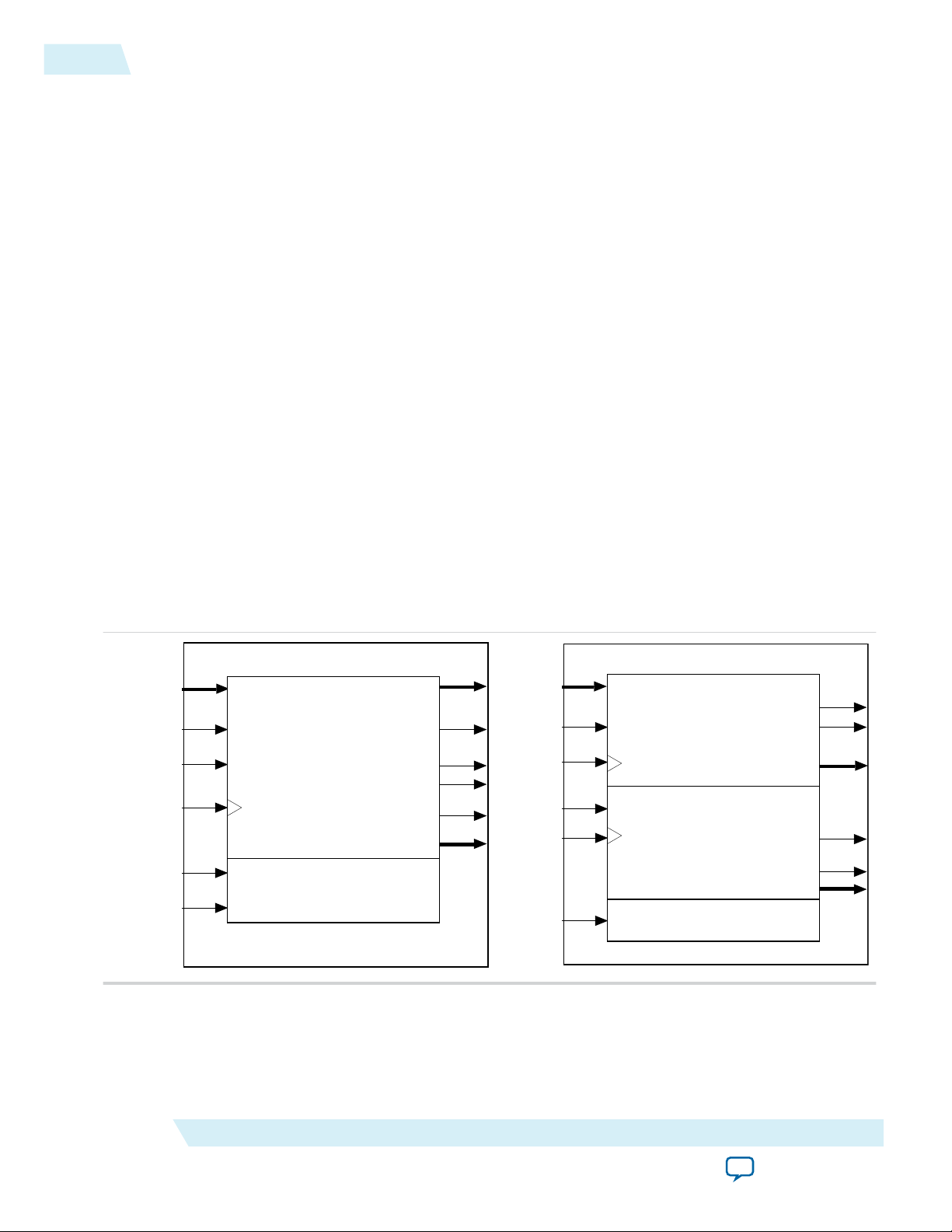
SCFIFO and DCFIFO Signals
This section provides diagrams of the SCFIFO and DCFIFO blocks to help in visualizing their input and
output ports. This section also describes each port in detail to help in understanding their usages,
functionality, or any restrictions. For better illustrations, some descriptions might refer you to a specific
section in this user guide.
UG-MFNALT_FIFO
2014.12.17
Figure 1: SCFIFO and DCFIFO IP Cores Input and Output Signals
For the SCFIFO block, the read and write signals are synchronized to the same clock; for the DCFIFO
block, the read and write signals are synchronized to the rdclk and wrclk clocks respectively. The
prefixes wr and rd represent the signals that are synchronized by the wrclk and rdclk clocks respectively.
Altera Corporation
SCFIFO and DCFIFO IP Cores User Guide
Send Feedback
Page 3

UG-MFNALT_FIFO
2014.12.17
SCFIFO and DCFIFO Signals
Table 2: Input and Output Ports Description
This table lists the signals of the IP cores. The term “series” refers to all the device families of a particular device.
For example, “Stratix series” refers to the Stratix®, Stratix GX, Stratix II, Stratix II GX, Stratix III, and new devices,
unless specified otherwise.
Port Type Required Description
(1)
clock
wrclk
(2)
Input Yes Positive-edge-triggered clock.
Input Yes Positive-edge-triggered clock.
Use to synchronize the following ports:
• data
• wrreq
• wrfull
• wrempty
• wrusedw
(2)
rdclk
Input Yes Positive-edge-triggered clock.
Use to synchronize the following ports:
• q
• rdreq
• rdfull
• rdempty
• rdusedw
3
(3)
data
Input Yes Holds the data to be written in the FIFO IP core when the
wrreq signal is asserted. If you manually instantiate the
FIFO IP core, ensure the port width is equal to the lpm_
width parameter.
(1)
Only applicable for the SCFIFO IP core.
(2)
Applicable for both of the DCFIFO IP cores.
(3)
Applicable for the SCFIFO, DCFIFO, and DCFIFO_MIXED_WIDTH IP cores.
SCFIFO and DCFIFO IP Cores User Guide
Send Feedback
Altera Corporation
Page 4
4
SCFIFO and DCFIFO Signals
Port Type Required Description
(3)
wrreq
UG-MFNALT_FIFO
2014.12.17
Input Yes Assert this signal to request for a write operation.
Ensure that the following conditions are met:
• Do not assert the wrreq signal when the full (for
SCFIFO) or wrfull (for DCFIFO) port is high. Enable
the overflow protection circuitry or set the overflow_
checking parameter to ON so that the FIFO IP core
can automatically disable the wrreq signal when it is
full.
• The wrreq signal must meet the functional timing
requirement based on the full or wrfull signal.
• Do not assert the wrreq signal during the deassertion
of the aclr signal. Violating this requirement creates a
race condition between the falling edge of the aclr
signal and the rising edge of the write clock if the
wrreq port is set to high. For both the DCFIFO IP
cores that target Stratix and Cyclone series (except
Stratix, Stratix GX, and Cyclone devices), you have the
option to automatically add a circuit to synchronize
the aclr signal with the wrclk clock, or set the write_
aclr_synch parameter to ON. Use this option to
ensure that the restriction is obeyed.
rdreq
sclr
aclr
(1)
(3)
(3)
Input Yes Assert this signal to request for a read operation. The
rdreq signal acts differently in normal mode and show-
ahead mode.
Ensure that the following conditions are met:
• Do not assert the rdreq signal when the empty (for
SCFIFO) or rdempty (for DCFIFO) port is high.
Enable the underflow protection circuitry or set the
underflow_checking parameter to ON so that the
FIFO IP core can automatically disable the rdreq
signal when it is empty.
• The rdreq signal must meet the functional timing
requirement based on the empty or rdempty signal.
Input No Assert this signal to clear all the output status ports, but
the effect on the q output may vary for different FIFO
configurations.
There are no minimum number of clock cycles for aclr
signals that must remain active.
Altera Corporation
SCFIFO and DCFIFO IP Cores User Guide
Send Feedback
Page 5
UG-MFNALT_FIFO
2014.12.17
q
full
wrfull
rdfull
Port Type Required Description
(3)
Output Yes Shows the data read from the read request operation.
For the SCFIFO IP core and DCFIFO IP core, the width
of the q port must be equal to the width of the data port.
If you manually instantiate the IP cores, ensure that the
port width is equal to the lpm_width parameter.
For the DCFIFO_MIXED_WIDTHS IP core, the width of
the q port can be different from the width of the data
port. If you manually instantiate the IP core, ensure that
the width of the q port is equal to the lpm_width_r
parameter. The IP core supports a wide write port with a
narrow read port, and vice versa. However, the width
ratio is restricted by the type of RAM block, and in
general, are in the power of 2.
(1)
(2)
(2)
, (4)
(4),
Output No When asserted, the FIFO IP core is considered full. Do
not perform write request operation when the FIFO IP
core is full.
In general, the rdfull signal is a delayed version of the
wrfull signal. However, for Stratix III devices and later,
the rdfull signal function as a combinational output
instead of a derived version of the wrfull signal.
Therefore, you must always refer to the wrfull port to
ensure whether or not a valid write request operation can
be performed, regardless of the target device.
SCFIFO and DCFIFO Signals
5
(1)
empty
wrempty
(4)
rdrempty
almost_full
almost_empty
(2)
, (4)
(1)
(1)
(2)
,
Output No When asserted, the FIFO IP core is considered empty. Do
not perform read request operation when the FIFO IP
core is empty.
In general, the wrempty signal is a delayed version of the
rdempty signal. However, for Stratix III devices and later,
the wrempty signal function as a combinational output
instead of a derived version of the rdempty signal.
Therefore, you must always refer to the rdempty port to
ensure whether or not a valid read request operation can
be performed, regardless of the target device.
Output No Asserted when the usedw signal is greater than or equal to
the almost_full_value parameter. It is used as an early
indication of the full signal.
Output No Asserted when the usedw signal is less than the almost_
empty_value parameter. It is used as an early indication
of the empty signal.
SCFIFO and DCFIFO IP Cores User Guide
Send Feedback
Altera Corporation
Page 6
6
SCFIFO and DCFIFO Parameters
Port Type Required Description
usedw
wrusedw
rdusedw
(1)
(2)
(2)
, (4)
, (4)
Output No Show the number of words stored in the FIFO.
Ensure that the port width is equal to the lpm_widthu
parameter if you manually instantiate the SCFIFO IP core
or the DCFIFO IP core. For the DCFIFO_MIXED_
UG-MFNALT_FIFO
WIDTH IP core, the width of the wrusedw and rdusedw
ports must be equal to the LPM_WIDTHU and lpm_widthu_
r parameters respectively.
For Stratix, Stratix GX, and Cyclone devices, the FIFO IP
core shows full even before the number of words stored
reaches its maximum value. Therefore, you must always
refer to the full or wrfull port for valid write request
operation, and the empty or rdempty port for valid read
request operation regardless of the target device.
The DCFIFO IP core rdempty output may momentarily glitch when the aclr input is asserted. To
prevent an external register from capturing this glitch incorrectly, ensure that one of the following is true:
• The external register must use the same reset which is connected to the aclr input of the DCFIFO IP
core, or
• The reset connected to the aclr input of the DCFIFO IP core must be asserted synchronous to the
clock which drives the external register.
2014.12.17
The output latency information of the FIFO IP cores is important, especially for the q output port,
because there is no output flag to indicate when the output is valid to be sampled.
SCFIFO and DCFIFO Parameters
This table lists the parameters for the SCFIFO and DCFIFO IP cores.
Parameter Type Requir
ed
lpm_width Integer Yes Specifies the width of the data and q ports for the
SCFIFO IP core and DCFIFO IP core. For the
DCFIFO_MIXED_WIDTHS IP core, this parameter
specifies only the width of the data port.
lpm_width_r Integer Yes Specifies the width of the q port for the DCFIFO_
MIXED_WIDTHS IP core.
lpm_widthu Integer Yes Specifies the width of the usedw port for the SCFIFO IP
core, or the width of the rdusedw and wrusedw ports
for the DCFIFO IP core. For the DCFIFO_MIXED_
WIDTHS IP core, it only represents the width of the
wrusedw port.
lpm_widthu_r
(4)
Integer Yes Specifies the width of the rdusedw port for the
DCFIFO_MIXED_WIDTHS IP core.
Description
(4)
Only applicable for the DCFIFO_MIXED_WIDTHS IP core.
Altera Corporation
SCFIFO and DCFIFO IP Cores User Guide
Send Feedback
Page 7

UG-MFNALT_FIFO
2014.12.17
SCFIFO and DCFIFO Parameters
7
Parameter Type Requir
ed
lpm_numwords Integer Yes Specifies the depths of the FIFO you require. The value
Description
must be at least 4.
The value assigned must comply with this equation,
2LPM_WIDTHU
lpm_showahead String Yes Specifies whether the FIFO is in normal mode (OFF) or
show-ahead mode (ON).
For normal mode, the FIFO IP core treats the rdreq
port as a normal read request that only performs read
operation when the port is asserted.
For show-ahead mode, the FIFO IP core treats the
rdreq port as a read-acknowledge that automatically
outputs the first word of valid data in the FIFO IP core
(when the empty or rdempty port is low) without
asserting the rdreq signal. Asserting the rdreq signal
causes the FIFO IP core to output the next data word, if
available.
If you set the parameter to ON, you may reduce
performance.
lpm_type
String No Identifies the library of parameterized modules (LPM)
entity name. The values are SCFIFO and DCFIFO.
maximize_speed Integer No Specifies whether or not to optimize for area or speed.
The values are 0 through 10. The values 0, 1, 2, 3, 4,
and 5 result in area optimization, while the values 6, 7,
8, 9, and 10 result in speed optimization.
This parameter is applicable for Cyclone II and
Stratix II devices only.
overflow_checking String No Specifies whether or not to enable the protection
circuitry for overflow checking that disables the wrreq
port when the FIFO IP core is full. The values are ON
or OFF. If omitted, the default is ON.
underflow_checking String No Specifies whether or not to enable the protection
circuitry for underflow checking that disables the rdreq
port when the FIFO IP core is empty. The values are
ON or OFF. If omitted, the default is ON.
Note that reading from an empty SCFIFO gives
unpredictable results.
(5)
Only applicable for the DCFIFO IP core.
SCFIFO and DCFIFO IP Cores User Guide
Send Feedback
Altera Corporation
Page 8
8
SCFIFO and DCFIFO Parameters
UG-MFNALT_FIFO
2014.12.17
Parameter Type Requir
delay_rdusedw
delay_wrusedw
(5)
(5)
ed
String No Specify the number of register stages that you want to
internally add to the rdusedw or wrusedw port using
the respective parameter.
Description
The default value of 1 adds a single register stage to the
output to improve its performance. Increasing the value
of the parameter does not increase the maximum
system speed. It only adds additional latency to the
respective output port.
add_usedw_msb_bit String No Increases the width of the rdusedw and wrusedw ports
by one bit. By increasing the width, it prevents the
FIFO IP core from rolling over to zero when it is full.
The values are ON or OFF. If omitted, the default value
is OFF.
This parameter is only applicable for Stratix and
Cyclone series (except for Stratix, Stratix GX, and
Cyclone devices).
rdsync_delaypipe
wrsync_delaypipe
(5)
(5)
Integer No Specify the number of synchronization stages in the
cross clock domain. The value of the rdsync_
delaypipe parameter relates the synchronization
stages from the write control logic to the read control
logic; the wrsync_delaypipe parameter relates the
synchronization stages from the read control logic to
the write control logic. Use these parameters to set the
number of synchronization stages if the clocks are not
synchronized, and set the clocks_are_synchronized
parameter to FALSE.
use_eab
Altera Corporation
The actual synchronization stage implemented relates
variously to the parameter value assigned, depends on
the target device.
For Cyclone II and Stratix II devices and later, the
values of these parameters are internally reduced by
two. Thus, the default value of 3 for these parameters
corresponds to a single synchronization stage; a value
of 4 results in two synchronization stages, and so on.
For these devices, choose at least 4 (two synchroniza‐
tion stages) for metastability protection.
String No Specifies whether or not the FIFO IP core is
constructed using the RAM blocks. The values are ON
or OFF.
Setting this parameter value to OFF yields the FIFO IP
core implemented in logic elements regardless of the
type of the TriMatrix memory block type assigned to
the ram_block_type parameter.
SCFIFO and DCFIFO IP Cores User Guide
Send Feedback
Page 9
UG-MFNALT_FIFO
2014.12.17
SCFIFO and DCFIFO Parameters
9
Parameter Type Requir
write_aclr_synch
(5)
ed
String No Specifies whether or not to add a circuit that causes the
aclr port to be internally synchronized by the wrclk
Description
clock. Adding the circuit prevents the race condition
between the wrreq and aclr ports that could corrupt
the FIFO IP core.
The values are ON or OFF. If omitted, the default value
is OFF. This parameter is only applicable for Stratix and
Cyclone series (except for Stratix, Stratix GX, and
Cyclone devices).
read_aclr_synch String No Specifies whether or not to add a circuit that causes the
aclr port to be internally synchronized by the rdclk
clock. Adding the circuit prevents the race condition
between the rdreq and aclr ports that could corrupt
the FIFO IP core.
The values are ON or OFF. If omitted, the default value
is OFF. This parameter is only applicable for families
beginning from Stratix III series.
clocks_are_synchron-
(5)
ized
String No Specifies whether or not the write and read clocks are
synchronized which in turn determines the number of
internal synchronization stages added for stable
operation of the FIFO. The values are TRUE and
FALSE. If omitted, the default value is FALSE. You
must only set the parameter to TRUE if the write clock
and the read clock are always synchronized and they
are multiples of each other. Otherwise, set this to
FALSE to avoid metastability problems.
ram_block_type
SCFIFO and DCFIFO IP Cores User Guide
If the clocks are not synchronized, set the parameter to
FALSE, and use the rdsync_delaypipe and wrsync_
delaypipe parameters to determine the number of
synchronization stages required.
String No Specifies the target device’s Trimatrix Memory Block to
be used. To get the proper implementation based on
the RAM configuration that you set, allow the
Quartus II software to automatically choose the
memory type by ignoring this parameter and set the
use_eab parameter to ON. This gives the compiler the
flexibility to place the memory function in any available
memory resource based on the FIFO depth required.
Altera Corporation
Send Feedback
Page 10

10
SCFIFO and DCFIFO Functional Timing Requirements
UG-MFNALT_FIFO
2014.12.17
Parameter Type Requir
ed
add_ram_output_register String No Specifies whether to register the q output. The values
Description
are ON and OFF. If omitted, the default value is OFF.
You can set the parameter to ON or OFF for the
SCFIFO or the DCFIFO, that do not target Stratix II,
Cyclone II, and new devices. This parameter does not
apply to these devices because the q output must be
registered in normal mode and unregistered in showahead mode for the DCFIFO.
almost_full_value Integer No Sets the threshold value for the almost_full port.
When the number of words stored in the FIFO IP core
is greater than or equal to this value, the almost_full
port is asserted.
almost_empty_value
(6)
Integer No Sets the threshold value for the almost_empty port.
When the number of words stored in the FIFO IP core
is less than this value, the almost_empty port is
asserted.
allow_wrcycle_when_full
(6)
String No Allows you to combine read and write cycles to an
already full SCFIFO, so that it remains full. The values
are ON and OFF. If omitted, the default is OFF. Use
only this parameter when the OVERFLOW_CHECKING
parameter is set to ON.
intended_device_family String No Specifies the intended device that matches the device
set in your Quartus II project. Use only this parameter
for functional simulation.
SCFIFO and DCFIFO Functional Timing Requirements
The wrreq signal is ignored (when FIFO is full) if you enable the overflow protection circuitry in the FIFO
parameter editor, or set the OVERFLOW_CHECKING parameter to ON. The rdreq signal is ignored (when
FIFO is empty) if you enable the underflow protection circuitry in the FIFO MegaWizard interface, or set
the UNDERFLOW_CHECKING parameter to ON.
If the protection circuitry is not enabled, you must meet the following functional timing requirements:
Table 3: Functional Timing Requirements
DCFIFO SCFIFO
Deassert the wrreq signal in the same clock cycle
when the wrfull signal is asserted.
Deassert the rdreq signal in the same clock cycle
when the rdempty signal is asserted. You must
observe these requirements regardless of expected
behavior based on wrclk and rdclk frequencies.
Deassert the wrreq signal in the same clock cycle
when the full signal is asserted.
Deassert the rdreq signal in the same clock cycle
when the empty signal is asserted.
(6)
Only applicable for the SCFIFO IP core.
Altera Corporation
SCFIFO and DCFIFO IP Cores User Guide
Send Feedback
Page 11
UG-MFNALT_FIFO
2014.12.17
Figure 2: Functional Timing for the wrreq Signal and the wrfull Signal
Figure 3: Functional Timing for the rdreq Signal and the rdempty Signal
SCFIFO and DCFIFO Output Status Flag and Latency
This figure shows the behavior for the wrreq and the wrfull signals.
This shows the behavior for the rdreq the rdempty signals.
11
The required functional timing for the DCFIFO as described previously is also applied to the SCFIFO.
The difference between the two modes is that for the SCFIFO, the wrreq signal must meet the functional
timing requirement based on the full signal and the rdreq signal must meet the functional timing
requirement based on the empty signal.
SCFIFO and DCFIFO Output Status Flag and Latency
The main concern in most FIFO design is the output latency of the read and write status signals.
SCFIFO and DCFIFO IP Cores User Guide
Send Feedback
Altera Corporation
Page 12

12
SCFIFO and DCFIFO Output Status Flag and Latency
UG-MFNALT_FIFO
2014.12.17
Table 4: Output Latency of the Status Flags for SCFIFO
This table shows the output latency of the write signal (wrreq) and read signal (rdreq) for the SCFIFO according
to the different output modes and optimization options.
Output Mode Optimization Option
(7)
wrreq / rdreq to full: 1
wrreq to empty: 2
Output Latency (in number of clock cycles)
(8)
Normal
(9)
Show-ahead
(9)
Speed
Area
Speed
Area
rdreq to empty: 1
wrreq / rdreq to usedw[]: 1
rdreq to q[]: 1
wrreq / rdreq to full: 1
wrreq / rdreq to empty : 1
wrreq / rdreq to usedw[] : 1
rdreq to q[]: 1
wrreq / rdreq to full: 1
wrreq to empty: 3
rdreq to empty: 1
wrreq / rdreq to usedw[]: 1
wrreq to q[]: 3
rdreq to q[]: 1
wrreq / rdreq to full: 1
wrreq to empty: 2
rdreq to empty: 1
wrreq / rdreq to usedw[]: 1
(7)
Speed optimization is equivalent to setting the ADD_RAM_OUTPUT_REGISTER parameter to ON. Setting the
parameter to OFF is equivalent to area optimization.
(8)
The information of the output latency is applicable for Stratix and Cyclone series only. It may not be
applicable for legacy devices such as the APEX® and FLEX® series.
(9)
For the Quartus II software versions earlier than 9.0, the normal output mode is called legacy output mode.
Normal output mode is equivalent to setting the LPM_SHOWAHEAD parameter to OFF. For Show-ahead mode,
the parameter is set to ON.
Altera Corporation
wrreq to q[]: 2
rdreq to q[]: 1
SCFIFO and DCFIFO IP Cores User Guide
Send Feedback
Page 13

UG-MFNALT_FIFO
2014.12.17
Table 5: LE Implemented RAM Mode for SCFIFO and DCFIFO
SCFIFO and DCFIFO Output Status Flag and Latency
13
Output Mode Optimization Option
Speed
Normal
(12)
Area
Show-ahead
(12)
Speed
(10)
wrreq / rdreq to full: 1
wrreq to empty: 2
rdreq to empty: 1
wrreq / rdreq to usedw[]: 1
rdreq to q[]: 1
wrreq / rdreq to full: 1
wrreq / rdreq to empty : 1
wrreq / rdreq to usedw[] : 1
rdreq to q[]: 1
wrreq / rdreq to full: 1
wrreq to empty: 3
rdreq to empty: 1
wrreq / rdreq to usedw[]: 1
wrreq to q[]: 1
rdreq to q[]: 1
Output Latency (in number of clock cycles)
(11)
wrreq / rdreq to full: 1
wrreq to empty: 2
rdreq to empty: 1
Area
wrreq / rdreq to usedw[]: 1
wrreq to q[]: 1
rdreq to q[]: 1
(10)
Speed optimization is equivalent to setting the ADD_RAM_OUTPUT_REGISTER parameter to ON. Setting the
parameter to OFF is equivalent to area optimization.
(11)
The information of the output latency is applicable for Stratix and Cyclone series only. It may not be
applicable for legacy devices such as the APEX® and FLEX® series.
(12)
For the Quartus II software versions earlier than 9.0, the normal output mode is called legacy output mode.
Normal output mode is equivalent to setting the LPM_SHOWAHEAD parameter to OFF. For Show-ahead mode,
the parameter is set to ON.
SCFIFO and DCFIFO IP Cores User Guide
Send Feedback
Altera Corporation
Page 14

14
SCFIFO and DCFIFO Metastability Protection and Related Options
Table 6: Output Latency of the Status Flag for the DCFIFO
This table shows the output latency of the write signal (wrreq) and read signal (rdreq) for the DCFIFO.
Output Latency (in number of clock cycles)
wrreq to wrfull: 1 wrclk
wrreq to rdfull: 2 wrclk cycles + following n rdclk
wrreq to wrempty: 1 wrclk
wrreq to rdempty: 2 wrclk
wrreq to wrusedw[]: 2 wrclk
wrreq to rdusedw[]: 2 wrclk + following n + 1 rdclk
wrreq to q[]: 1 wrclk + following 1 rdclk
rdreq to rdempty: 1 rdclk
rdreq to wrempty: 1 rdclk + following n wrclk
rdreq to rfull: 1 rdclk
rdreq to wrfull: 1 rdclk + following n wrclk
rdreq to rdusedw[]: 2 rdclk
rdreq to wrusedw[]: 1 rdclk + following n + 1 wrclk
(15)
+ following n rdclk
(15)
(15)
(15)
(15)
(15)
(15)
(13)
UG-MFNALT_FIFO
2014.12.17
rdreq to q[]: 1 rdclk
SCFIFO and DCFIFO Metastability Protection and Related Options
The FIFO parameter editor provides the total latency, clock synchronization, metastability protection,
area, and f
Table 7: DCFIFO Group Setting for Latency and Related Options
This table shows the available group setting.
Lowest latency but requires synchronized clocks This option uses one synchronization stage with no
(13)
The output latency information is only applicable for Arria® GX, Stratix, and Cyclone series (except for
Stratix, Stratix GX, Hardcopy® Stratix, and Cyclone devices). It might not be applicable for legacy devices,
such as APEX and FLEX series of devices.
(14)
The number of n cycles for rdclk and wrclk is equivalent to the number of synchronization stages and are
related to the WRSYNC_DELAYPIPE and RDSYNC_DELAYPIPE parameters. For more information about how the
actual synchronization stage (n) is related to the parameters set for different target device, refer to
(15)
This is applied only to Show-ahead output modes. Show-ahead output mode is equivalent to setting the
LPM_SHOWAHEAD parameter to ON
options as a group setting for the DCFIFO.
MAX
Group Setting Comment
metastability protection. It uses the smallest size
and provides good f
MAX
.
Select this option if the read and write clocks are
related clocks.
Altera Corporation
SCFIFO and DCFIFO IP Cores User Guide
Send Feedback
Page 15

UG-MFNALT_FIFO
2014.12.17
Group Setting Comment
SCFIFO and DCFIFO Metastability Protection and Related Options
Minimal setting for unsynchronized clocks This option uses two synchronization stages with
good metastability protection. It uses the medium
Best metastability protection, best f
unsynchronized clocks
max
and
size and provides good f
This option uses three or more synchronization
stages with the best metastability protection. It uses
the largest size but gives the best f
MAX
.
.
MAX
The group setting for latency and related options is available through the FIFO parameter editor. The
setting mainly determines the number of synchronization stages, depending on the group setting you
select. You can also set the number of synchronization stages you desire through the WRSYNC_DELAYPIPE
and RDSYNC_DELAYPIPE parameters, but you must understand how the actual number of synchronization
stages relates to the parameter values set in different target devices.
The number of synchronization stages set is related to the value of the WRSYNC_DELAYPIPE and
RDSYNC_DELAYPIPE pipeline parameters. For some cases, these pipeline parameters are internally scaled
down by two to reflect the actual synchronization stage.
Table 8: Relationship between the Actual Synchronization Stage and the Pipeline Parameters for Different
Target Devices
This table shows the relationship between the actual synchronization stage and the pipeline parameters.
Stratix II, Cyclone II, and later Stratix and Cyclone
Devices in Low-Latency
Version
(16)
Actual synchronization stage = value of pipeline parameter - 2
(17)
Actual synchronization stage = value
Other Devices
of pipeline parameter
15
The TimeQuest timing analyzer includes the capability to estimate the robustness of asynchronous
transfers in your design, and to generate a report that details the mean time between failures (MTBF) for
all detected synchronization register chains. This report includes the MTBF analysis on the synchroniza‐
tion pipeline you applied between the asynchronous clock domains in your DCFIFO. You can then decide
the number of synchronization stages to use in order to meet the range of the MTBF specification you
require.
Related Information
• Area and Timing Optimization
Provides information about enabling metastability analysis and reporting.
• http://www.altera.com/literature/hb/qts/qts_qii53018.pdf
Provides information about enabling metastability analysis and reporting.
(16)
You can obtain the low-latency of the DCFIFO (for Stratix, Stratix GX, and Cyclone devices) when the
clocks are not set to synchronized in Show-ahead mode with unregistered output in the FIFO parameter
editor. The corresponding parameter settings for the low-latency version are ADD_RAM_OUTPUT_
REGISTER=OFF, LPM_SHOWAHEAD=ON, and CLOCKS_ARE_SYNCHRONIZED=FALSE. These parameter settings are
only applicable to Stratix, Stratix GX, and Cyclone devices.
(17)
The values assigned to WRSYNC_DELAYPIPE and RDSYNC_DELAYPIPE parameters are internally reduced by 2
to represent the actual synchronization stage implemented. Thus, the default value 3 for these parameters
corresponds to a single synchronization pipe stage; a value of 4 results in 2 synchronization stages, and so
on. For these devices, choose 4 (2 synchronization stages) for metastability protection.
SCFIFO and DCFIFO IP Cores User Guide
Send Feedback
Altera Corporation
Page 16

16
SCFIFO and DCFIFO Synchronous Clear and Asynchronous Clear Effect
UG-MFNALT_FIFO
SCFIFO and DCFIFO Synchronous Clear and Asynchronous Clear Effect
The FIFO IP cores support the synchronous clear (sclr) and asynchronous clear (aclr) signals,
depending on the FIFO modes. The effects of these signals are varied for different FIFO configurations.
The SCFIFO supports both synchronous and asynchronous clear signals while the DCFIFO support
asynchronous clear signal and asynchronous clear signal that synchronized with the write and read clocks.
Table 9: Synchronous Clear and Asynchronous Clear in the SCFIFO
This table shows the synchronous clear and asynchronous clear signals supported in the SCFIFO.
Mode Synchronous Clear (sclr)
Deasserts the full and almost_full signals.
(18)
Asynchronous Clear (aclr)
(18)
2014.12.17
Effects on status ports
Commencement of effects upon
assertion
Effects on the q output for normal
output modes
Effects on the q output for showahead output modes
Asserts the empty and almost_empty signals.
Resets the usedw flag.
At the rising edge of the
Immediate (except for the q output)
clock.
The read pointer is reset
and points to the first data
The q output remains at its previous
value.
location. If the q output is
not registered, the output
shows the first data word
of the SCFIFO; otherwise,
the q output remains at its
previous value.
The read pointer is reset
and points to the first data
location. If the q output is
not registered, the output
remains at its previous
value for only one clock
cycle and shows the first
If the q output is not registered, the
output shows the first data word of
the SCFIFO starting at the first rising
clock edge.
Otherwise, the q output remains its
previous value.
data word of the SCFIFO
at the next rising clock
(19)
edge.
(19)
(18)
The read and write pointers reset to zero upon assertion of either the sclr or aclr signal.
(19)
The first data word shown after the reset is not a valid Show-ahead data. It reflects the data where the read
pointer is pointing to because the q output is not registered. To obtain a valid Show-ahead data, perform a
valid write after the reset.
Altera Corporation
Otherwise, the q output
remains at its previous
value.
SCFIFO and DCFIFO IP Cores User Guide
Send Feedback
Page 17

UG-MFNALT_FIFO
2014.12.17
SCFIFO and DCFIFO Synchronous Clear and Asynchronous Clear Effect
Table 10: Asynchronous Clear in DCFIFO
This table shows the asynchronous clear supported by the DCFIFO.
Mode Asynchronous Clear
(aclr)
aclr (synchronize
with write clock)
(21)
aclr (synchronize with read clock)
(20)
,
(22)
(23)
,
17
Effects on status ports
Commencement of effects
upon assertion
Effects on the q output for
normal output modes
(24)
Effect on the q output for
show-ahead output
modes
(24)
Deasserts the wrfull
signal.
The wrfull signal is
asserted while the
write domain is
clearing which
nominally takes
three cycles of the
write clock after the
The rdempty signal is
asserted while the read
domain is clearing which
nominally takes three cycles
of the read clock after the
asynchronous release of the
aclr input.
asynchronous release
of the aclr input.
Deasserts the rdfull signal.
Asserts the wrempty and rdempty signals.
Resets the wrusedw and rdusedw flags.
Immediate.
The output remains unchanged if it is not registered. If the port is
registered, it is cleared.
The output shows 'X' if it is not registered. If the port is registered, it is
cleared.
(20)
The wrreq signal must be low when the DCFIFO comes out of reset (the instant when the aclr signal is
deasserted) at the rising edge of the write clock to avoid a race condition between write and reset. If this
condition cannot be guaranteed in your design, the aclr signal needs to be synchronized with the write
clock. This can be done by setting the Add circuit to synchronize 'aclr' input with 'wrclk' option from the
FIFO parameter editor, or setting the WRITE_ACLR_SYNCH parameter to ON.
(21)
Even though the aclr signal is synchronized with the write clock, asserting the aclr signal still affects all the
status flags asynchronously.
(22)
The rdreq signal must be low when the DCFIFO comes out of reset (the instant when the aclr signal is
deasserted) at the rising edge of the read clock to avoid a race condition between read and reset. If this
condition cannot be guaranteed in your design, the aclr signal needs to be synchronized with the read
clock. This can be done by setting the Add circuit to synchronize 'aclr' input with 'rdclk' option from the
FIFO parameter editor, or setting the READ_ACLR_SYNCH parameter to ON.
(23)
Even though the aclr signal is synchronized with the read clock, asserting the aclr signal affects all the
status flags asynchronously.
(24)
For Stratix and Cyclone series (except Stratix, Stratix GX, and Cyclone devices), the DCFIFO only supports
registered q output in Normal mode, and unregistered q output in Show-ahead mode. For other devices, you
have an option to register or unregister the q output (regardless of the Normal mode or Show-ahead mode)
in the FIFO parameter editor or set through the ADD_RAM_OUTPUT_REGISTER parameter.
SCFIFO and DCFIFO IP Cores User Guide
Send Feedback
Altera Corporation
Page 18

18
Recovery and Removal Timing Violation Warnings when Compiling a DCFIFO IP Core
UG-MFNALT_FIFO
Recovery and Removal Timing Violation Warnings when Compiling a DCFIFO IP
Core
During compilation of a design that contains a DCFIFO IP core, the Quartus II software may issue
recovery and removal timing violation warnings.
You may safely ignore warnings that represent transfers from aclr to the read side clock domain. To
ensure that the design meets timing, enable the ACLR synchronizer for both read and write domains.
To enable the ACLR synchronizer for both read and write domains, on the DCFIFO 2 tab of the FIFO
MegaWizard Plug-In Manager, turn on Asynchronous clear, Add circuit to synchronize ‘aclr’ input
with ‘wrclk’, and Add circuit to synchronize ‘aclr’ input with ‘rdclk’.
Note: For correct timing analysis, Altera recommends enabling the Removal and Recovery Analysis
option in the TimeQuest timing analyzer tool when you use the aclr signal. The analysis is turned
on by default in the TimeQuest timing analyzer tool.
Different Input and Output Width
The DCFIFO_MIXED_WIDTHS IP core supports different write input data and read output data widths
if the width ratio is valid. The FIFO parameter editor prompts an error message if the combinations of the
input and the output data widths produce an invalid ratio. The supported width ratio in a power of 2 and
depends on the RAM.
2014.12.17
The IP core supports a wide write port with a narrow read port, and vice versa.
Figure 4: Writing 16-bit Words and Reading 8-bit Words
This figure shows an example of a wide write port (16-bit input) and a narrow read port (8-bit output).
In this example, the read port is operating at twice the frequency of the write port. Writing two 16-bit
words to the FIFO buffer increases the wrusedw flag to two and the rusedw flag to four. Four 8-bit read
operations empty the FIFO buffer. The read begins with the least-significant 8 bits from the 16-bit word
written followed by the most-significant 8 bits.
Altera Corporation
SCFIFO and DCFIFO IP Cores User Guide
Send Feedback
Page 19

UG-MFNALT_FIFO
2014.12.17
Figure 5: Writing 8-Bit Words and Reading 16-Bit Words
Constraint Settings
19
This figure shows an example of a narrow write port (8-bit input) with a wide read port (16-bit output).
In this example, the read port is operating at half the frequency of the write port. Writing four 8-bit words
to the FIFO buffer increases the wrusedw flag to four and the rusedw flag to two. Two 16-bit read
operations empty the FIFO. The first and second 8-bit word written are equivalent to the LSB and MSB of
the 16-bit output words, respectively. The rdempty signal stays asserted until enough words are written on
the narrow write port to fill an entire word on the wide read port.
Constraint Settings
When using the Quartus II TimeQuest timing analyzer with a design that contains a DCFIFO block apply
the following false paths to avoid timing failures in the synchronization registers:
• For paths crossing from the write into the read domain, apply a false path assignment between the
delayed_wrptr_g and rs_dgwp registers:
set_false_path -from [get_registers {*dcfifo*delayed_wrptr_g[*]}] -to [get_registers
{*dcfifo*rs_dgwp*}]
• For paths crossing from the read into the write domain, apply a false path assignment between the
rdptr_g and ws_dgrp registers:
set_false_path -from [get_registers {*dcfifo*rdptr_g[*]}] -to [get_registers
{*dcfifo*ws_dgrp*}]
The false path assignments are automatically added through the HDL-embedded Synopsis design
constraint (SDC) commands when you compile your design. The related message is shown under the
TimeQuest timing analyzer report.
Note:
If you use the Quartus II Classic timing analyzer, the false paths are applied automatically for the
DCFIFO.
Note:
The constraints are internally applied but are not written to the Synopsis Design Constraint File
(.sdc). To view the embedded-false path, type report_sdc in the console pane of the TimeQuest
timing analyzer GUI.
If the DCFIFO is implemented in logic elements (LEs), you can ignore the cross-domain timing
violations from the data path of the DFFE array (that makes up the memory block) to the q output
SCFIFO and DCFIFO IP Cores User Guide
Send Feedback
Altera Corporation
Page 20

20
Coding Example for Manual Instantiation
register. To ensure the q output is valid, sample the output only after the rdempty signal is
deasserted.
Related Information
Quartus II TimeQuest Timing Analyzer
Provides information about setting the timing constraint
Coding Example for Manual Instantiation
This section provides a Verilog HDL coding example to instantiate the DCFIFO IP core. It is not a
complete coding for you to compile, but it provides a guideline and some comments for the required
structure of the instantiation. You can use the same structure to instantiate other IP cores but only with
the ports and parameters that are applicable to the IP cores you instantiated.
Table 11: Verilog HDL Coding Example to Instantiate the DCFIFO IP Core
//module declaration
module dcfifo8x32 (aclr, data, …… ,wfull);
//Module's port declarations input aclr;
input [31:0] data;
.
.
output wrfull;
//Module’s data type declarations and assignments wire rdempty_w;
.
.
wire wrfull = wrfull_w; wire [31:0] q = q_w;
/*Instantiates dcfifo megafunction. Must declare all the ports available from the
megafunction and
define the connection to the module's ports.
Refer to the ports specification from the user guide for more information about the
megafunction's
ports*/
//syntax: <megafunction's name> <given an instance name> dcfifo inst1 (
//syntax: .<dcfifo's megafunction's port>(<module's port/wire>)
.wrclk (wrclk),
.rdclk (rdreq),
.
.
.wrusedw ()); //left the output open if it's not used
/*Start with the keyword “defparam”, defines the parameters and value assignments.
Refer to
parameters specifications from the user guide for more information about the megafunction's
parameters*/
defparam
//syntax: <instance name>.<parameter> = <value> inst1.intended_device_family =
"Stratix III",
inst1.lpm_numwords = 8,
.
.
inst1.wrsync_delaypipe = 4;
endmodule
UG-MFNALT_FIFO
2014.12.17
Altera Corporation
SCFIFO and DCFIFO IP Cores User Guide
Send Feedback
Page 21

ROM
256 x 32
trclk
trclk
32
32
fifo_in
fifo_wrreq
fifo_wrfull
trclk
8
rom_out
rom_addr
Write
Control Logic
DCFIFO
8 x 32
Read
Control Logic
RAM
256 x 32
32
fifo_out
32
ram_in
32
q
9
word_count
8
ram_addr
fifo_rdreq
fifo_rdempty
rvclk
rvclk rvclk
ram_wren
ram_rden
UG-MFNALT_FIFO
2014.12.17
Design Example
In this design example, the data from the ROM is required to be transferred to the RAM. Assuming the
ROM and RAM are driven by non-related clocks, you can use the DCFIFO to transfer the data between
the asynchronous clock domains effectively.
Figure 6: Component Blocks and Signal Interaction
This figure shows the component blocks and their signal interactions.
Design Example
21
Note: Both the DCFIFO IP cores are only capable of handling asynchronous data transferring issues
(metastable effects). You must have a controller to govern and monitor the data buffering process
between the ROM, DCFIFO, and RAM. This design example provides you the write control logic
(write_control_logic.v), and the read control logic (read_control_logic.v) which are compiled with the
DCFIFO specifications that control the valid write or read request to or from the DCFIFO.
Note: This design example is validated with its functional behavior, but without timing analysis and gate-
level simulation. The design coding such as the state machine for the write and read controllers
may not be optimized. The intention of this design example is to show the use the IP core, particu‐
larly on its control signal in data buffering application, rather than the design coding and verifica‐
tion processes.
To obtain the DCFIFO settings in this design example, refer to the parameter settings from the design file
(dcfifo8x32.v).
The following sections include separate simulation waveforms to describe how the write and read control
logics generate the control signal with respect to the signal received from the DCFIFO.
Note:
For better understanding, refer to the signal names in Figure 6 on page 25 when you go through the
descriptions for the simulation waveforms.
SCFIFO and DCFIFO IP Cores User Guide
Send Feedback
Altera Corporation
Page 22

22
Design Example
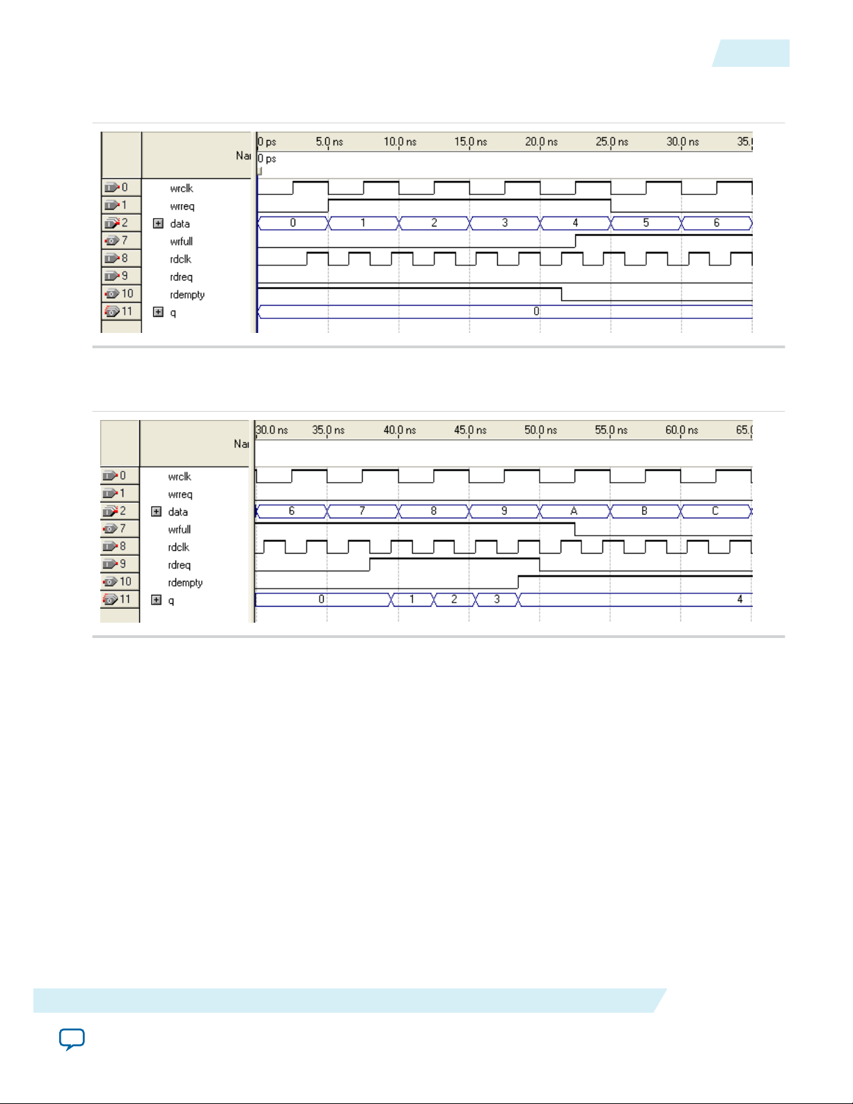
Figure 7: Initial Write Operation to the DCFIFO IP Core
Table 12: Initial Write Operation to the DCFIFO IP Core Waveform Description
State Description
UG-MFNALT_FIFO
2014.12.17
IDLE
Before reaching 10 ns, the reset signal is high and causes the write controller to be in
the IDLE state. In the IDLE state, the write controller drives the fifo_wrreq signal to
low, and requests the data to be read from rom_addr=00. The ROM is configured to
have an unregistered output, so that the rom_out signal immediately shows the data
from the rom_addr signal regardless of the reset. This shortens the latency because the
rom_out signal is connected directly to the fifo_in signal, which is a registered input
port in the DCFIFO. In this case, the data (00000001) is always stable and pending to be
written into the DCFIFO when the fifo_wrreq signal is high during the WRITE state.
WRITE
The write controller transitions from the IDLE state to the WRITE state if the fifo_
wrfull signal is low after the reset signal is deasserted. In the WRITE state, the write
controller drives the fifo_wrreq signal to high, and requests for write operation to the
DCFIFO. The rom_addr signal is unchanged (00) so the data is stable for at least one
clock cycle before the DCFIFO actually writes in the data at the next rising clock edge.
INCADR
The write controller transitions from the WRITE state to the INCADR state, if the rom_
addr signal has not yet increased to ff (that is, the last data from the ROM has not been
read out). In the INDADR state, the write controller drives the fifo_wrreq signal to low,
and increases the rom_addr signal by 1 (00 to 01).
- The same state transition continues as stated in IDLE and WRITE states, if the fifo_
wrfull signal is low and the rom_addr signal not yet increased to ff.
Altera Corporation
SCFIFO and DCFIFO IP Cores User Guide
Send Feedback
Page 23

UG-MFNALT_FIFO
2014.12.17
Figure 8: Initial Read Operation from the DCFIFO IP Core
Table 13: Initial Read Operation from the DCFIFO IP Core Waveform Description
State Description
Design Example
23
IDLE
INCADR
WRITE
--
Before reaching 35 ns, the read controller is in the IDLE state because the fifo_rdempty
signal is high even when the reset signal is low (not shown in the waveform). In the IDLE
state, the ram_addr = ff to accommodate the increment of the RAM address in the
INCADR state, so that the first data read is stored at ram_addr = 00 in the WRITE state.
The read controller transitions from the IDLE state to the INCADR state, if the fifo_
rdempty signal is low. In the INCADR state, the read controller drives the fifo_rdreq
signal to high, and requests for read operation from the DCFIFO. The ram_addr signal is
increased by one (ff to 00), so that the read data can be written into the RAM at ram_
addr = 00.
From the INCADR state, the read controller always transition to the WRITE state at the next
rising clock edge. In the WRITE state, it drives the ram_wren signal to high, and enables the
data writing into the RAM at ram_addr = 00. At the same time, the read controller drives
the ram_rden signal to high so that the newly written data is output at q at the next rising
clock edge. Also, it increases the word_count signal to 1 to indicate the number of words
successfully read from the DCFIFO.
The same state transition continues as stated in INCADR and WRITE states, if the fifo_
rdempty signal is low.
SCFIFO and DCFIFO IP Cores User Guide
Send Feedback
Altera Corporation
Page 24

24
Design Example
Figure 9: Write Operation when DCFIFO is FULL
Table 14: Write Operation when DCFIFO is FULL Waveform Description
State Description
UG-MFNALT_FIFO
2014.12.17
INCADR
When the write controller is in the INCADR state, and the fifo_wrfull signal is asserted,
the write controller transitions to the WAIT state in the next rising clock edge.
WAIT
In the WAIT state, the write controller holds the rom_addr signal (08) so that the
respective data is written into the DCFIFO when the write controller transitions to the
WRITE state.
The write controller stays in WAIT state if the fifo_wrfull signal is still high. When the
fifo_wrfull is low, the write controller always transitions from the WAIT state to the
WRITE state at the next rising clock edge.
WRITE
In the WRITE state, then only the write controller drives the fifo_wrreq signal to high, and
requests for write operation to write the data from the previously held address (08) into
the DCFIFO. It always transitions to the INCADR state in the next rising clock edge, if the
rom_addr signal has not yet increased to ff.
--
The same state transition continues as stated in INCADR, WAIT, and WRITE states, if the
fifo_wrfull signal is high.
Figure 10: Completion of Data Transfer from ROM to DCFIFO
Altera Corporation
SCFIFO and DCFIFO IP Cores User Guide
Send Feedback
Page 25

UG-MFNALT_FIFO
2014.12.17
Table 15: Completion of Data Transfer from ROM to DCFIFO Waveform Description
State Description
WRITE When the write controller is in the WRITE state, and rom_addr = ff, the write controller
drives the fifo_wrreq signal to high to request for last write operation to DCFIFO. The
data 100 is the last data stored in the ROM to be written into the DCFIFO. In the next
rising clock edge, the write controller transitions to the DONE state.
DONE In the DONE state, the write controller drives the fifo_wrreq signal to low.
-- The fifo_wrfull signal is deasserted because the read controller in the receiving domain
continuously performs the read operation. However, the fifo_wrfull signal is only
deasserted sometime after the read request from the receiving domain. This is due to the
latency in the DCFIFO (rdreq signal to wrfull signal).
Figure 11: Completion of Data Transfer from DCFIFO to RAM
Design Example
25
The fifo_rdempty signal is asserted to indicate that the DCFIFO is empty. The read controller drives the
fifo_rdreq signal to low, and enables the write of the last data 100 at ram_addr =ff. The word_count
signal is increased to 256 (in decimal) to indicate that all the 256 words of data from the ROM are success‐
fully transferred to the RAM.
The last data written into the RAM is shown at the q output.
Note:
To verify the results, compare the q outputs with the data in rom_initdata.hex file provided in the
design example. Open the file in the Quartus II software and select the word size as 32 bit. The q
output must display the same data as in the file.
Related Information
DCFIFO Design Example
Provides all the design files including the testbench. The zip file also includes the .do script
(dcfifo_de_top.do) that automates functional simulation that you can use to run the simulation using the
ModelSim-Altera software
SCFIFO and DCFIFO IP Cores User Guide
Send Feedback
Altera Corporation
Page 26

26
Gray-Code Counter Transfer at the Clock Domain Crossing
Gray-Code Counter Transfer at the Clock Domain Crossing
This section describes the effect of the large skew between Gray-code counter bits transfers at the clock
domain crossing (CDC) with recommended solution. The gray-code counter is 1-bit transition occurs
while other bits remain stable when transferring data from the write domain to the read domain and vice
versa. If the destination domain latches on the data within the metastable range (violating setup or hold
time), only 1 bit is uncertain and destination domain reads the counter value as either an old counter or a
new counter. In this case, the DCFIFO still works, as long as the counter sequence is not corrupted.
The following section shows an example of how large skew between GNU C compiler (GCC) bits can
corrupt the counter sequence. Taking a counter width with 3-bit wide and assuming it is transferred from
write clock domain to read clock domain. Assume all the counter bits have 0 delay relative to the destina‐
tion clock, excluding the bit[0] that has delay of 1 clock period of source clock. That is, the skew of the
counter bits will be 1 clock period of the source clock when they arrived at the destination registers.
The following shows the correct gray-code counter sequence:
000,
001,
011,
010,
110....
UG-MFNALT_FIFO
2014.12.17
which then transfers the data to the read domain, and on to the destination bus registers.
Because of the skew for bit[0], the destination bus registers receive the following sequence:
000,
000,
011,
011,
110....
Because of the skew, a 2-bit transition occurs. This sequence is acceptable if the timing is met. If the 2-bit
transition occurs and both bits violate timing, it may result in the counter bus settled at a future or
previous counter value, which will corrupt the DCFIFO.
Therefore, the skew must be within a certain skew to ensure that the sequence is not corrupted.
Related Information
skew_report.tcl
Use the skew_report.tcl to analyze the actual skew and required skew in your design
Document Revision History
This table lists the document revision history for this user guide.
Altera Corporation
SCFIFO and DCFIFO IP Cores User Guide
Send Feedback
Page 27

UG-MFNALT_FIFO
2014.12.17
Table 16: Document Revision History
Date Version Changes
Document Revision History
27
December 2014 2014.12.17
May 2013 8.2
August 2012 8.1
• Clarified that there are no minimum number of
clock cycles for aclr signals that must remain
active.
• Added Recovery and Removal Timing Violation
Warnings when Compiling a DCFIFO Megafunc‐
tion section.
• Removed a note about ignoring any recovery and
removal violation reported in the TimeQuest
timing analyzer that represent transfers from the
aclr to the read side clock domain in Synchronous
Clear and Asynchronous Clear Effect section.
• Updated Table 8 on page 20 to state that both the
read and write pointers reset to zero upon
assertion of either the sclr or aclr signal.
• Updated Table 1 on page 7 to note that the
wrusedw, rdusedw, wrfull, rdfull wrempty and
rdempty values are subject to the latencies listed
in Table 5 on page 18.
• Included a link to skew_report.tcl “Gray-Code
Counter Transfer at the Clock Domain Crossing”
on page 29.
August 2012 8.0
• Updated “DCFIFO” on page 3, “Ports Specifica‐
tions” on page 6, “Functional Timing Require‐
ments” on page 14, “Synchronous Clear and
Asynchronous Clear Effect” on page 20.
• Updated Table 1 on page 7, Table 2 on page 10,
Table 9 on page 21.
• Added Table 4 on page 16.
• Renamed and updated “DCFIFO Clock Domain
Crossing Timing Violation” to “Gray-Code
Counter Transfer at the Clock Domain Crossing”
on page 29.
February 2012 7.0
• Updated the notes for Table 4 on page 16.
• Added the “DCFIFO Clock Domain Crossing
Timing Violation” section.
September 2010 6.2 Added prototype and component declarations.
SCFIFO and DCFIFO IP Cores User Guide
Send Feedback
Altera Corporation
Page 28

28
Document Revision History
Date Version Changes
UG-MFNALT_FIFO
2014.12.17
January 2010 6.1
• Updated “Functional Timing Requirements”
section.
• Minor changes to the text.
September 2009 6.0
• Replaced “FIFO Megafunction Features” section
with “Configuration Methods”.
• Updated “Input and Output Ports”.
• Added “Parameter Specifications”, “Output Status
Flags and Latency”, “Metastability Protection and
Related Options”, “Constraint Settings”, “Coding
Example for Manual Instantiation”, and “Design
Example”.
February 2009 5.1 Minor update in Table 8 on page 17.
January 2009 5.0 Complete re-write of the user guide.
May 2007 4.0
• Added support for Arria GX devices.
• Updated for new GUI.
• Added six design examples in place of functional
description.
• Reorganized and updated Chapter 3 to have
separate tables for the SCFIFO and DCFIFO
megafunctions.
• Added Referenced Documents section.
March 2007 3.3
• Minor content changes, including adding
Stratix III and Cyclone III information
• Re-took screenshots for software version 7.0
September 2005 3.2 Minor content changes.
Altera Corporation
SCFIFO and DCFIFO IP Cores User Guide
Send Feedback
 Loading...