


 Loading...
Allwinner Technology CO., Ltd. |
A13 |
|
|
A13 Datasheet
V1.12
2012.3.29
A13 Datasheet v1.12
Copyright © 2011-2012 Allwinner Technology. All Rights Reserved. 2012-03-29

Allwinner Technology CO., Ltd. |
A13 |
|
|
Revision History
Version |
Date |
Section/ Page |
Changes |
|
|
|
|
V1.00 |
2011.12.9 |
|
Initial version |
|
|
|
|
|
|
|
GPIOE[0]/[1]/[2] and GPIOG[0]/[1]/[2] |
V1.10 |
2011.12.30 |
Pin Description |
|
|
|
|
are changed for INPUT only. |
|
|
|
|
V1.11 |
2012.1.10 |
Pin Dimension |
Pin Dimension |
|
|
|
|
V1.12 |
2012.3.29 |
Audio Codec |
Revise some description |
|
|
|
|
A13 Datasheet v1.12
Copyright © 2011-2012 Allwinner Technology. All Rights Reserved. 1 2012-03-29

|
|
Allwinner Technology CO., Ltd. |
A13 |
|
|
|
|
|
|
|
|
Table of Contents |
|
|
Revision History ...................................................................................................................... |
1 |
|||
1. |
Introduction ..................................................................................................................... |
5 |
||
2. |
Feature............................................................................................................................. |
5 |
||
3. |
Functional Block Diagram................................................................................................ |
9 |
||
4. |
Pin Assignment............................................................................................................... |
10 |
||
4.1. |
Pin Map ................................................................................................................... |
10 |
||
4.2. |
Pin Dimension ........................................................................................................... |
11 |
||
5. |
Pin Description............................................................................................................... |
12 |
||
5.1. |
Pin Characteristics .................................................................................................... |
12 |
||
5.2. |
Multiplexing Characteristics ...................................................................................... |
23 |
||
5.3. |
Power and Miscellaneous Signals............................................................................... |
26 |
||
6. |
Electrical Characteristics ............................................................................................... |
29 |
||
6.1. |
Absolute Maximum Ratings ...................................................................................... |
29 |
||
6.2. |
Recommended Operating Conditions ......................................................................... |
29 |
||
6.3. |
DC Electrical Characteristics ..................................................................................... |
30 |
||
6.4. |
Oscillator Electrical Characteristics ............................................................................ |
31 |
||
6.5. |
Power up/down and Reset Specifications .................................................................... |
31 |
||
7. |
PWM.............................................................................................................................. |
33 |
||
7.1. |
Overview ................................................................................................................. |
33 |
||
7.2. |
PWM Signal Description........................................................................................... |
33 |
||
8. |
Async Timer Controller.................................................................................................. |
34 |
||
8.1. |
Overview ................................................................................................................. |
34 |
||
9. |
Sync Timer Controller.................................................................................................... |
34 |
||
9.1. |
Overview ................................................................................................................. |
34 |
||
10. |
Interrupt Controller ....................................................................................................... |
35 |
||
10.1. |
Overview ................................................................................................................. |
35 |
||
10.2. |
External Interrupt Signal Description.......................................................................... |
35 |
||
11. |
DMA Controller ............................................................................................................. |
37 |
||
11.1. |
Overview ................................................................................................................. |
37 |
||
12. |
SDRAM Controller ........................................................................................................ |
38 |
||
A13 Datasheet v1.12 |
|
|
||
Copyright © 2011-2012 Allwinner Technology. All Rights Reserved. |
2 |
|
||
2012-03-29 |
|
|
||

|
|
Allwinner Technology CO., Ltd. |
A13 |
|
|
|
|
|
|
12.1. |
Overview ................................................................................................................. |
38 |
||
12.2. |
SDRAM Signal Description....................................................................................... |
38 |
||
13. |
NAND Flash Controller.................................................................................................. |
41 |
||
13.1. |
Overview ................................................................................................................. |
41 |
||
13.2. NAND Flash Controller Signal Description ................................................................ |
42 |
|||
14. |
SD3.0 Controller............................................................................................................. |
43 |
||
14.1. |
Overview ................................................................................................................. |
43 |
||
14.2. SD3.0 Controller Signal Description .......................................................................... |
44 |
|||
15. |
Two Wire Interface......................................................................................................... |
45 |
||
15.1. |
Overview ................................................................................................................. |
45 |
||
15.2. TWI Controller Signal Description............................................................................. |
45 |
|||
16. |
SPI Interface .................................................................................................................. |
47 |
||
16.1. |
Overview ................................................................................................................. |
47 |
||
16.2. SPI Controller Signal Description .............................................................................. |
47 |
|||
17. |
UART Interface.............................................................................................................. |
48 |
||
17.1. |
Overview ................................................................................................................. |
48 |
||
17.2. UART Controller Signal Description .......................................................................... |
49 |
|||
18. |
CIR Interface ................................................................................................................. |
50 |
||
18.1. |
Overview ................................................................................................................. |
50 |
||
18.2. CIR Controller Signal Description.............................................................................. |
50 |
|||
19. |
USB OTG Controller...................................................................................................... |
51 |
||
19.1. |
Overview ................................................................................................................. |
51 |
||
19.2. USB OTG Controller Signal Description .................................................................... |
51 |
|||
20. |
USB HOST Controller.................................................................................................... |
52 |
||
20.1. |
Overview ................................................................................................................. |
52 |
||
20.2. USB HOST Controller Signal Description .................................................................. |
52 |
|||
21. |
Audio Codec................................................................................................................... |
53 |
||
21.1. |
Overview ................................................................................................................. |
53 |
||
21.2. Audio Codec Signal Description ................................................................................ |
53 |
|||
22. |
LRADC .......................................................................................................................... |
54 |
||
22.1. |
Overview ................................................................................................................. |
54 |
||
22.2. |
LRADC Signal Description ....................................................................................... |
54 |
||
A13 Datasheet v1.12 |
|
|
||
Copyright © 2011-2012 Allwinner Technology. All Rights Reserved. |
3 |
|
||
2012-03-29 |
|
|
||

|
|
Allwinner Technology CO., Ltd. |
A13 |
|
|
|
|
|
|
23. |
Touch Panel Controller................................................................................................... |
55 |
||
23.1. |
Overview ................................................................................................................. |
55 |
||
23.2. Touch Panel Signal Description ................................................................................. |
55 |
|||
24. |
Camera Sensor Interface ................................................................................................ |
56 |
||
24.1. |
Overview ................................................................................................................. |
56 |
||
24.2. |
CSI Signal Description .............................................................................................. |
56 |
||
25. |
Universal LCD/TV Timing Controller ............................................................................ |
57 |
||
25.1. |
Overview ................................................................................................................. |
57 |
||
25.2. |
LCD Signal Description ............................................................................................ |
57 |
||
26. |
Port Controller............................................................................................................... |
58 |
||
26.1. |
Port Description........................................................................................................ |
58 |
||
27. |
Declaration..................................................................................................................... |
59 |
||
A13 Datasheet v1.12
Copyright © 2011-2012 Allwinner Technology. All Rights Reserved. 4 2012-03-29

Allwinner Technology CO., Ltd. |
A13 |
|
|
1.Introduction
Allwinner Tech has expanded its processor lineup to include a new ARM Cortex-A8 chip A13 which is even more competitive for Android tablets with higher performance (ManyCore Lite), lower power consumption, and lower total system cost. As the brains of Android 4.0, A13 makes multitasking smoother, apps loading more quickly, and anything you touch responds instantly. What‟s more important, A13 is available in eLQFP176 package with Audio Codec and R-TP integrated.
2.Feature
CPU
ARM Cortex-A8 Core
32KB I-Cache/32KB D-Cache/256KB L2 Cache
Using NEON for video, audio, and graphic workloads eases the burden of supporting more dedicated accelerators across the SoC and enables the system to support the standards of tomorrow
RCT JAVA-Accelerations to optimize just in time(JIT) and dynamitic adaptive compilation(DAC), and reduces memory footprint up to three times
GPU
3D Graphic Engine
Support Open GL ES 1.1/ 2.0 and open VG 1.1
VPU
Video Decoding (FULL HD)
Support all popular video formats, including VP6/8, AVS, H.264, H.263 , MPEG-1/2/4,
A13 Datasheet v1.12
Copyright © 2011-2012 Allwinner Technology. All Rights Reserved. 5 2012-03-29

Allwinner Technology CO., Ltd. |
A13 |
|
|
etc
Support 1920*1080@ 30fps in all formats
Video Encoding
Support encoding in H.264 MP format
Up to 1920*1080@30fps
Display Processing Ability
Four moveable and size-adjustable layers
Support multi-format image input
Support image enhancement processor
Support Alpha blending /anti-flicker
Support Hardware cursor
Support output color correction (luminance / hue / saturation etc)
Display Output Ability
Flexible LCD interface (CPU / Sync RGB )
Image Input Ability
Camera sensor interface (CSI)
Memory
16-bit SDRAM controller
Support DDR2 SDRAM and DDR3 SDRAM up to 533MHz
Memory Capacity up to 512MB
8-bit NAND Flash Controller with 2 CE and 2 RB signals
Support SLC/MLC/TLC/DDR NAND
A13 Datasheet v1.12
Copyright © 2011-2012 Allwinner Technology. All Rights Reserved. 6 2012-03-29

Allwinner Technology CO., Ltd. |
A13 |
|
|
64-bit ECC
Peripherals
One USB 2.0 OTG controller for general application and one USB EHCI/OHCI controller for host application
Three high-speed memory controllers supporting SD version 3.0 and eMMC version 4.3
One UART with only TX/RX and one UART with RTS/CTS
Three SPI controllers
Three Two-Wire Interfaces
IR controller supporting CIR remoter
6-bit LRADC for line control
Internal 4-wire touch panel controller with pressure sensor and 2-point touch
Internal 24-bit Audio Codec for 2-Ch headphone and 1-Ch microphone
PWM controller
System
8-Ch normal DMA and 8-Ch dedicated DMA
Internal 48K SRAM on chip
6 asynchronic timers, 2 synchronic timers, 1 watchdog, and 2 AVS counters
Security
Security System
Support DES/3DES/AES encryption and decryption.
Support SHA-1, MD5 message digest
Support 160-bit hardware PRNG with 192-bit seed
128-bit EFUSE chip ID
A13 Datasheet v1.12
Copyright © 2011-2012 Allwinner Technology. All Rights Reserved. 7 2012-03-29

Allwinner Technology CO., Ltd. |
A13 |
|
|
Package
eLQFP176 package
A13 Datasheet v1.12
Copyright © 2011-2012 Allwinner Technology. All Rights Reserved. 8 2012-03-29
Allwinner Technology CO., Ltd. |
A13 |
|
|
3.Functional Block Diagram
DDR2/3
|
AUDIO |
SDC/MMC |
NAND/eMMC |
DRAMC |
|
ADC |
FLASH |
||
|
|
|
||
|
EARPHONE |
|
|
|
|
AMP |
|
CPU |
CSI |
|
|
|
|
|
G-SENSOR |
TWI |
|
Cotex A8 |
|
|
|
2 Point |
||
|
SPI |
|
|
|
|
|
|
RTP |
|
ALS |
UART |
|
|
|
|
|
|
||
|
GPIO |
GPU |
VPU |
JTAG |
|
Mali 400 |
1080P CODEC |
||
|
|
|
||
|
|
|
|
32.768K |
|
|
USB |
USB |
RTC |
|
KEY |
SYSTEM |
||
|
OTG |
HOST |
||
|
|
|||
|
|
24M |
||
|
|
|
|
Crystal |
|
|
|
|
PMU |
|
|
|
|
SYSTEM |
Figure 3. A13 Block Diagram
A13 Datasheet v1.12
Copyright © 2011-2012 Allwinner Technology. All Rights Reserved. 9 2012-03-29

Allwinner Technology CO., Ltd. |
A13 |
|
|
4.Pin Assignment
4.1.Pin Map
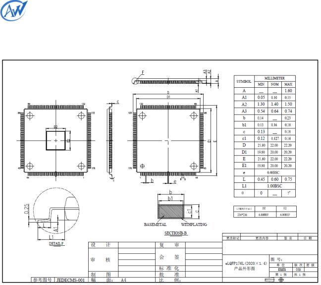
Figure 4-1. A13 eLQFP 176 Package
A13 Datasheet v1.12
Copyright © 2011-2012 Allwinner Technology. All Rights Reserved. 10 2012-03-29
Allwinner Technology CO., Ltd. |
A13 |
|
|
4.2.Pin Dimension
Figure 4-2. A13 Pin Dimension
A13 Datasheet v1.12
Copyright © 2011-2012 Allwinner Technology. All Rights Reserved. 11 2012-03-29

Allwinner Technology CO., Ltd. |
A13 |
|
|
5.Pin Description
5.1.Pin Characteristics
1.Pin Number: Ball numbers on the bottom side associated with each signals on the bottom.
2.Pin Name: Names of signals multiplexed on each pin No. (also notice that the name of the pin is the signal name in function 0).
3.Type: signal direction
- |
I |
= Input |
- |
O |
= Output |
- |
I/O |
= Input/Output |
- |
A |
= Analog |
- |
AIO |
= Analog Input/Output |
- PWR |
= Power |
|
- GND |
= Ground |
|
4.Pin Reset State: The state of the terminal at reset (power up).
-0: The buffer drives VOL(pull down/pull up resistor not activated)
-0 (PD): The buffer drives VOL with an active pull down resistor.
-1: The buffer drives VOH (pull down/pull up resistor not activated).
-1 (PU): The buffer drives VOH with an active pull up resistor.
- Z: High-impedance
-L: High-impedance with an active pull down resistor.
-H: High-impedance with an active pull up resistor.
5.Pull Up/Down: Denotes the presence of an internal pull up or pull down resister. Pull up and pull down resistor can be enabled or disabled via software.
6.Buffer Strength: Drive strength of the associated output buffer.
7.Note that the P[B:G] in the following table stands for GPIO [B:G].
A13 Datasheet v1.12
Copyright © 2011-2012 Allwinner Technology. All Rights Reserved. 12 2012-03-29

Allwinner Technology CO., Ltd. |
A13 |
|
|
Pin No. |
|
Pin Name |
|
Type |
|
Pin Reset State |
|
|
Pull |
Buffer |
|
|
|
|
|||||||
|
|
|
|
|
|
|
||||
|
|
|
|
|
|
|
|
|
Up/Down |
Strength |
|
|
|
|
|
|
|
|
|||
|
|
|
|
|
|
|
|
|
|
|
|
|
NRE |
O |
|
|
|
|
|
|
|
1 |
|
|
|
|
|
|
|
|
|
|
|
PC5 |
|
|
|
|
|
|
|
||
|
|
|
|
|
|
|
|
|
||
|
|
|
|
|
|
|
|
|
|
|
|
|
NCE0 |
O |
|
|
|
|
Pull-up |
|
|
2 |
|
|
|
|
|
|
|
|
|
|
|
PC4 |
|
|
|
|
|
|
|
||
|
|
|
|
|
|
|
|
|
||
|
|
|
|
|
|
|
|
|
|
|
|
|
NCE1 |
O |
|
|
|
|
Pull-up |
|
|
|
|
|
|
|
|
|
|
|
|
|
3 |
|
SPI0_CS0 |
|
|
|
|
|
|
|
|
|
|
|
|
|
|
|
|
|
|
|
|
|
PC3 |
|
|
|
|
|
|
|
|
|
|
|
|
|
|
|
|
|
|
|
4 |
|
VDD1_CPU |
PWR |
|
|
|
|
|
|
|
|
|
|
|
|
|
|
|
|
|
|
5 |
|
VCC1 |
PWR |
|
|
|
|
|
|
|
|
|
|
|
|
|
|
|
|
|
|
|
|
NCLE |
O |
|
|
|
|
|
|
|
|
|
|
|
|
|
|
|
|
|
|
6 |
|
SPI0_CLK |
|
|
|
|
|
|
|
|
|
|
|
|
|
|
|
|
|
|
|
|
|
PC2 |
|
|
|
|
|
|
|
|
|
|
|
|
|
|
|
|
|
|
|
|
|
NALE |
O |
|
|
|
|
|
|
|
|
|
|
|
|
|
|
|
|
|
|
7 |
|
SPI0_MISO |
|
|
|
|
|
|
|
|
|
|
|
|
|
|
|
|
|
|
|
|
|
PC1 |
|
|
|
|
|
|
|
|
|
|
|
|
|
|
|
|
|
|
|
|
|
NWE |
O |
|
|
|
|
|
|
|
|
|
|
|
|
|
|
|
|
|
|
8 |
|
SPI0_MOSI |
|
|
|
|
|
|
|
|
|
|
|
|
|
|
|
|
|
|
|
|
|
PC0 |
|
|
|
|
|
|
|
|
|
|
|
|
|
|
|
|
|
|
|
9 |
|
VDD2_CPU |
PWR |
|
|
|
|
|
|
|
|
|
|
|
|
|
|
|
|
|
|
|
|
PB10 |
I/O |
|
|
|
|
|
|
|
10 |
|
|
|
|
|
|
|
|
|
|
|
EINT24 |
|
|
|
|
|
|
|
||
|
|
|
|
|
|
|
|
|
||
|
|
|
|
|
|
|
|
|
|
|
11 |
|
VDD3_CPU |
PWR |
|
|
|
|
|
|
|
|
|
|
|
|
|
|
|
|
|
|
|
|
PG9 |
I/O |
|
|
|
|
|
|
|
|
|
|
|
|
|
|
|
|
|
|
12 |
|
SPI1_CS0 |
|
|
|
|
|
|
|
|
|
|
|
|
|
|
|
|
|
|
|
|
|
UART3_TX |
|
|
|
|
|
|
|
|
|
|
|
|
|
|
|
|
|
|
|
A13 Datasheet v1.12
Copyright © 2011-2012 Allwinner Technology. All Rights Reserved. 13 2012-03-29

|
|
Allwinner Technology CO., Ltd. |
A13 |
|
||||
|
|
|
|
|
|
|
|
|
|
|
|
EINT9 |
|
|
|
|
|
|
|
|
|
|
|
|
|
|
|
|
|
|
|
|
|
|
|
|
|
|
PG10 |
I/O |
|
|
|
|
|
|
|
|
|
|
|
|
|
|
|
|
SPI1_CLK |
|
|
|
|
|
|
13 |
|
|
|
|
|
|
|
|
|
UART3_RX |
|
|
|
|
|
|
|
|
|
|
|
|
|
|
|
|
|
|
|
|
|
|
|
|
|
|
|
EINT10 |
|
|
|
|
|
|
|
|
|
|
|
|
|
|
|
|
|
PG11 |
I/O |
|
|
|
|
|
|
|
|
|
|
|
|
|
|
|
|
SPI1_MOSI |
|
|
|
|
|
|
14 |
|
|
|
|
|
|
|
|
|
UART3_CTS |
|
|
|
|
|
|
|
|
|
|
|
|
|
|
|
|
|
|
|
|
|
|
|
|
|
|
|
EINT11 |
|
|
|
|
|
|
|
|
|
|
|
|
|
|
|
|
|
PG12 |
I/O |
|
|
|
|
|
|
|
|
|
|
|
|
|
|
|
|
SPI1_MISO |
|
|
|
|
|
|
15 |
|
|
|
|
|
|
|
|
|
UART3_RTS |
|
|
|
|
|
|
|
|
|
|
|
|
|
|
|
|
|
|
|
|
|
|
|
|
|
|
|
EINT12 |
|
|
|
|
|
|
|
|
|
|
|
|
|
|
|
16 |
|
VDD4_CPU |
PWR |
|
|
|
|
|
|
|
|
|
|
|
|
|
|
17 |
|
DZQ |
A |
|
|
|
|
|
|
|
|
|
|
|
|
|
|
18 |
|
SVREF |
P |
|
|
|
|
|
|
|
|
|
|
|
|
|
|
19 |
|
DDR3_D4 |
I/O |
|
|
|
|
|
|
|
|
|
|
|
|
|
|
20 |
|
DDR3_D6 |
I/O |
|
|
|
|
|
|
|
|
|
|
|
|
|
|
21 |
|
DDR3_D2 |
I/O |
|
|
|
|
|
|
|
|
|
|
|
|
|
|
22 |
|
DDR3_D0 |
I/O |
|
|
|
|
|
|
|
|
|
|
|
|
|
|
23 |
|
VCC1_DRAM |
PWR |
|
|
|
|
|
|
|
|
|
|
|
|
|
|
24 |
|
DDR3_D11 |
I/O |
|
|
|
|
|
|
|
|
|
|
|
|
|
|
25 |
|
DDR3_D9 |
I/O |
|
|
|
|
|
|
|
|
|
|
|
|
|
|
26 |
|
DDR3_D13 |
I/O |
|
|
|
|
|
|
|
|
|
|
|
|
|
|
27 |
|
DDR3_D15 |
I/O |
|
|
|
|
|
|
|
|
|
|
|
|
|
|
28 |
|
DDR3_DM1 |
O |
|
|
|
|
|
|
|
|
|
|
|
|
|
|
29 |
|
DDR3_DM0 |
O |
|
|
|
|
|
|
|
|
|
|
|
|
|
|
30 |
|
VCC2_DRAM |
PWR |
|
|
|
|
|
|
|
|
|
|
|
|
|
|
31 |
|
DDR3_DQS0 |
I/O |
|
|
|
|
|
|
|
|
|
|
|
|
|
A13 Datasheet v1.12
Copyright © 2011-2012 Allwinner Technology. All Rights Reserved. 14 2012-03-29

|
|
Allwinner Technology CO., Ltd. |
A13 |
|
|||||
|
|
|
|
|
|
|
|
|
|
|
32 |
|
DDR3_DQS0_N |
|
I/O |
|
|
|
|
|
|
|
|
|
|
|
|||
|
|
|
|
|
|
|
|
|
|
|
33 |
|
DDR3_DQS1 |
|
I/O |
|
|
|
|
|
|
|
|
|
|
|
|
|
|
|
34 |
|
DDR3_DQS1_N |
|
I/O |
|
|
|
|
|
|
|
|
|
|
|
|
|
|
|
35 |
|
VDD1_INT |
|
PWR |
|
|
|
|
|
|
|
|
|
|
|
|
|
|
|
36 |
|
DDR3_D12 |
|
I/O |
|
|
|
|
|
|
|
|
|
|
|
|
|
|
|
37 |
|
DDR3_D8 |
|
I/O |
|
|
|
|
|
|
|
|
|
|
|
|
|
|
|
38 |
|
DDR3_D14 |
|
I/O |
|
|
|
|
|
|
|
|
|
|
|
|
|
|
|
39 |
|
DDR3_D10 |
|
I/O |
|
|
|
|
|
|
|
|
|
|
|
|
|
|
|
40 |
|
DDR3_D1 |
|
I/O |
|
|
|
|
|
|
|
|
|
|
|
|
|
|
|
41 |
|
DDR3_D3 |
|
I/O |
|
|
|
|
|
|
|
|
|
|
|
|
|
|
|
42 |
|
DDR3_D7 |
|
I/O |
|
|
|
|
|
|
|
|
|
|
|
|
|
|
|
43 |
|
VCC3_DRAM |
|
PWR |
|
|
|
|
|
|
|
|
|
|
|
|
|
|
|
44 |
|
DDR3_D5 |
|
I/O |
|
|
|
|
|
|
|
|
|
|
|
|
|
|
|
45 |
|
DDR3_CK |
|
O |
|
|
|
|
|
|
|
|
|
|
|
|
|
|
|
46 |
|
DDR3_CK_N |
|
O |
|
|
|
|
|
|
|
|
|
|
|
|
|
|
|
47 |
|
DDR3_CKE |
|
O |
|
|
|
|
|
|
|
|
|
|
|
|
|
|
|
48 |
|
DDR3_A10 |
|
O |
|
|
|
|
|
|
|
|
|
|
|
|
|
|
|
49 |
|
DDR3_BA1 |
|
O |
|
|
|
|
|
|
|
|
|
|
|
|
|
|
|
50 |
|
DDR3_A12 |
|
O |
|
|
|
|
|
|
|
|
|
|
|
|
|
|
|
51 |
|
DDR3_A4 |
|
O |
|
|
|
|
|
|
|
|
|
|
|
|
|
|
|
52 |
|
DDR3_A1 |
|
O |
|
|
|
|
|
|
|
|
|
|
|
|
|
|
|
53 |
|
VCC4_DRAM |
|
PWR |
|
|
|
|
|
|
|
|
|
|
|
|
|
|
|
54 |
|
DDR3_A6 |
|
O |
|
|
|
|
|
|
|
|
|
|
|
|
|
|
|
55 |
|
DDR3_A8 |
|
O |
|
|
|
|
|
|
|
|
|
|
|
|
|
|
|
56 |
|
DDR3_A11 |
|
O |
|
|
|
|
|
|
|
|
|
|
|
|
|
|
|
57 |
|
DDR3_A14 |
|
O |
|
|
|
|
|
|
|
|
|
|
|
|
|
|
|
58 |
|
DDR3_RAS |
|
O |
|
|
|
|
|
|
|
|
|
|
|
|
|
|
|
59 |
|
DDR3_CAS |
|
O |
|
|
|
|
|
|
|
|
|
|
|
|
|
|
|
60 |
|
DDR3_WE |
|
O |
|
|
|
|
|
|
|
|
|
|
|
|
|
|
A13 Datasheet v1.12
Copyright © 2011-2012 Allwinner Technology. All Rights Reserved. 15 2012-03-29

|
|
Allwinner Technology CO., Ltd. |
A13 |
|
|||||
|
|
|
|
|
|
|
|
|
|
|
61 |
|
DDR3_BA2 |
|
O |
|
|
|
|
|
|
|
|
|
|
|
|||
|
|
|
|
|
|
|
|
|
|
|
62 |
|
VCC5_DRAM |
|
PWR |
|
|
|
|
|
|
|
|
|
|
|
|
|
|
|
63 |
|
DDR3_BA0 |
|
O |
|
|
|
|
|
|
|
|
|
|
|
|
|
|
|
64 |
|
DDR3_A0 |
|
O |
|
|
|
|
|
|
|
|
|
|
|
|
|
|
|
65 |
|
DDR3_A3 |
|
O |
|
|
|
|
|
|
|
|
|
|
|
|
|
|
|
66 |
|
DDR3_A2 |
|
O |
|
|
|
|
|
|
|
|
|
|
|
|
|
|
|
67 |
|
DDR3_A5 |
|
O |
|
|
|
|
|
|
|
|
|
|
|
|
|
|
|
68 |
|
DDR3_A13 |
|
O |
|
|
|
|
|
|
|
|
|
|
|
|
|
|
|
69 |
|
DDR3_A9 |
|
O |
|
|
|
|
|
|
|
|
|
|
|
|
|
|
|
70 |
|
DDR3_RST |
|
O |
|
|
|
|
|
|
|
|
|
|
|
|
|
|
|
71 |
|
DDR3_A7 |
|
O |
|
|
|
|
|
|
|
|
|
|
|
|
|
|
|
72 |
|
DDR3_ODT |
|
O |
|
|
|
|
|
|
|
|
|
|
|
|
|
|
|
73 |
|
VDD2_INT |
|
PWR |
|
|
|
|
|
|
|
|
|
|
|
|
|
|
|
74 |
|
HPOUTL |
|
O |
|
|
|
|
|
|
|
|
|
|
|
|
|
|
|
75 |
|
HPBP |
|
O |
|
|
|
|
|
|
|
|
|
|
|
|
|
|
|
76 |
|
V33_HP |
|
PWR |
|
|
|
|
|
|
|
|
|
|
|
|
|
|
|
77 |
|
HPCOM |
|
O |
|
|
|
|
|
|
|
|
|
|
|
|
|
|
|
78 |
|
HPOUTR |
|
O |
|
|
|
|
|
|
|
|
|
|
|
|
|
|
|
79 |
|
AGND |
|
GND |
|
|
|
|
|
|
|
|
|
|
|
|
|
|
|
80 |
|
VRP |
|
A |
|
|
|
|
|
|
|
|
|
|
|
|
|
|
|
81 |
|
AVCC |
|
PWR |
|
|
|
|
|
|
|
|
|
|
|
|
|
|
|
82 |
|
VRA2 |
|
A |
|
|
|
|
|
|
|
|
|
|
|
|
|
|
|
83 |
|
VRA1 |
|
A |
|
|
|
|
|
|
|
|
|
|
|
|
|
|
|
84 |
|
MICIN1 |
|
I |
|
|
|
|
|
|
|
|
|
|
|
|
|
|
|
85 |
|
VMIC |
|
PWR |
|
|
|
|
|
|
|
|
|
|
|
|
|
|
|
86 |
|
LRADC |
|
I |
|
|
|
|
|
|
|
|
|
|
|
|
|
|
|
87 |
|
TPX2 |
|
I |
|
|
|
|
|
|
|
|
|
|
|
|
|
|
|
88 |
|
TPY2 |
|
I |
|
|
|
|
|
|
|
|
|
|
|
|
|
|
|
89 |
|
TPX1 |
|
I |
|
|
|
|
|
|
|
|
|
|
|
|
|
|
A13 Datasheet v1.12
Copyright © 2011-2012 Allwinner Technology. All Rights Reserved. 16 2012-03-29

|
|
Allwinner Technology CO., Ltd. |
A13 |
|
|||||
|
|
|
|
|
|
|
|
|
|
|
90 |
|
TPY1 |
|
I |
|
|
|
|
|
|
|
|
|
|
|
|||
|
|
|
|
|
|
|
|
|
|
|
91 |
|
X24MOUT |
|
O |
|
|
|
|
|
|
|
|
|
|
|
|
|
|
|
92 |
|
X24MIN |
|
I |
|
|
|
|
|
|
|
|
|
|
|
|
|
|
|
93 |
|
UDM0 |
|
I/O |
|
|
|
|
|
|
|
|
|
|
|
|
|
|
|
94 |
|
UDP0 |
|
I/O |
|
|
|
|
|
|
|
|
|
|
|
|
|
|
|
95 |
|
UDM1 |
|
I/O |
|
|
|
|
|
|
|
|
|
|
|
|
|
|
|
96 |
|
UDP1 |
|
I/O |
|
|
|
|
|
|
|
|
|
|
|
|
|
|
|
97 |
|
V33_USB |
|
PWR |
|
|
|
|
|
|
|
|
|
|
|
|
|
|
|
98 |
|
VDD3-INT |
|
PWR |
|
|
|
|
|
|
|
|
|
|
|
|
|
|
|
99 |
|
NC |
|
|
|
|
|
|
|
|
|
|
|
|
|
|
|
|
|
100 |
|
VCC2 |
|
PWR |
|
|
|
|
|
|
|
|
|
|
|
|
|
|
|
|
|
TWI0-SCK |
|
I/O |
|
|
|
|
|
101 |
|
|
|
|
|
|
|
|
|
|
PB0 |
|
|
|
|
|
|
|
|
|
|
|
|
|
|
|
|
|
|
|
|
|
|
|
|
|
|
|
|
|
|
TWI0-SDA |
|
I/O |
|
|
|
|
|
102 |
|
|
|
|
|
|
|
|
|
|
PB1 |
|
|
|
|
|
|
|
|
|
|
|
|
|
|
|
|
|
|
|
|
|
|
|
|
|
|
|
|
103 |
|
PB2/EINT16 |
|
I/O |
|
|
|
|
|
|
|
|
|
|
|
|
|
|
|
104 |
|
PB4/EINT18 |
|
I/O |
|
|
|
|
|
|
|
|
|
|
|
|
|
|
|
105 |
|
PB15 |
|
I/O |
|
|
|
|
|
|
|
|
|
|
|
|
|
|
|
106 |
|
PB16 |
|
I/O |
|
|
|
|
|
|
|
|
|
|
|
|
|
|
|
|
|
SDC0_D1 |
|
I/O |
|
|
|
|
|
107 |
|
|
|
|
|
|
|
|
|
|
PF0 |
|
|
|
|
|
|
|
|
|
|
|
|
|
|
|
|
|
|
|
|
|
|
|
|
|
|
|
|
|
|
SDC0_D0 |
|
I/O |
|
|
|
|
|
108 |
|
|
|
|
|
|
|
|
|
|
PF1 |
|
|
|
|
|
|
|
|
|
|
|
|
|
|
|
|
|
|
|
|
|
|
|
|
|
|
|
|
109 |
|
VDD4_INT |
|
PWR |
|
|
|
|
|
|
|
|
|
|
|
|
|
|
|
|
|
SDC0_CLK |
|
I/O |
|
|
|
|
|
110 |
|
|
|
|
|
|
|
|
|
|
PF2 |
|
|
|
|
|
|
|
|
|
|
|
|
|
|
|
|
|
|
|
|
|
|
|
|
|
|
|
|
|
|
SDC0_CMD |
|
I/O |
|
|
|
|
|
111 |
|
|
|
|
|
|
|
|
|
|
PF3 |
|
|
|
|
|
|
|
|
|
|
|
|
|
|
|
|
|
|
|
|
|
|
|
|
|
|
|
|
112 |
|
SDC0_D3 |
|
|
|
|
|
|
|
|
|
|
|
|
|
|
|
|
A13 Datasheet v1.12
Copyright © 2011-2012 Allwinner Technology. All Rights Reserved. 17 2012-03-29

|
|
Allwinner Technology CO., Ltd. |
A13 |
|
||||
|
|
|
|
|
|
|
|
|
|
|
|
PF4 |
|
|
|
|
|
|
|
|
|
|
|
|
|
|
|
|
|
|
|
|
|
|
|
|
|
|
SDC0_D2 |
|
|
|
|
|
|
113 |
|
|
|
|
|
|
|
|
|
PF5 |
|
|
|
|
|
|
|
|
|
|
|
|
|
|
|
|
|
|
|
|
|
|
|
|
|
|
|
CSI_PCLK |
I/O |
|
|
|
|
|
|
|
|
|
|
|
|
|
|
|
|
SPI2_CS0 |
|
|
|
|
|
|
114 |
|
|
|
|
|
|
|
|
|
EINT14 |
|
|
|
|
|
|
|
|
|
|
|
|
|
|
|
|
|
|
|
|
|
|
|
|
|
|
|
PE0 |
|
|
|
|
|
|
|
|
|
|
|
|
|
|
|
|
|
CSI_MCLK |
I/O |
|
|
|
|
|
|
|
|
|
|
|
|
|
|
|
|
SPI2_CLK |
|
|
|
|
|
|
115 |
|
|
|
|
|
|
|
|
|
EINT15 |
|
|
|
|
|
|
|
|
|
|
|
|
|
|
|
|
|
|
|
|
|
|
|
|
|
|
|
PE1 |
|
|
|
|
|
|
|
|
|
|
|
|
|
|
|
|
|
CSI_HSYNC |
I/O |
|
|
|
|
|
|
|
|
|
|
|
|
|
|
116 |
|
SPI2_MOSI |
|
|
|
|
|
|
|
|
|
|
|
|
|
|
|
|
|
PE2 |
|
|
|
|
|
|
|
|
|
|
|
|
|
|
|
|
|
CSI_VSYNC |
I/O |
|
|
|
|
|
|
|
|
|
|
|
|
|
|
117 |
|
SPI2_MISO |
|
|
|
|
|
|
|
|
|
|
|
|
|
|
|
|
|
PE3 |
|
|
|
|
|
|
|
|
|
|
|
|
|
|
|
|
|
CSI_D0 |
I/O |
|
|
|
|
|
|
|
|
|
|
|
|
|
|
118 |
|
SDC2_D0 |
|
|
|
|
|
|
|
|
|
|
|
|
|
|
|
|
|
PE4 |
|
|
|
|
|
|
|
|
|
|
|
|
|
|
|
|
|
CSI_D1 |
I/O |
|
|
|
|
|
|
|
|
|
|
|
|
|
|
119 |
|
SDC2_D1 |
|
|
|
|
|
|
|
|
|
|
|
|
|
|
|
|
|
PE5 |
|
|
|
|
|
|
|
|
|
|
|
|
|
|
|
|
|
CSI_D2 |
I/O |
|
|
|
|
|
|
|
|
|
|
|
|
|
|
120 |
|
SDC2_D2 |
|
|
|
|
|
|
|
|
|
|
|
|
|
|
|
|
|
PE6 |
|
|
|
|
|
|
|
|
|
|
|
|
|
|
|
|
|
CSI_D3 |
I/O |
|
|
|
|
|
|
|
|
|
|
|
|
|
|
121 |
|
SDC2_D3 |
|
|
|
|
|
|
|
|
|
|
|
|
|
|
|
|
|
PE7 |
|
|
|
|
|
|
|
|
|
|
|
|
|
|
A13 Datasheet v1.12
Copyright © 2011-2012 Allwinner Technology. All Rights Reserved. 18 2012-03-29
Loading...