

Allwinner A10 Schematics

Confidential
Allwinner Technology CO., Ltd. A10
A10 Datasheet
V1.21
2012.4.6
A10 Datasheet V1.21
Copyright © 2011-2012 Allwinner Technology. All Rights Reserved.
2012-04-06

Confidential
Allwinner Technology CO., Ltd. A10
Version
Date
Section/ Page
Changes compared to previous issue
V1.00
2011-8-22
Initial version
V1.10
2012-2-17
Page 79
LCD/tv timing controller overview
V1.20
2012-3-29
Audio Codec
Revise some description
V1.21
2012-4-6
USB
Revise some USB description
Revision History
A10 Datasheet V1.21
Copyright © 2011-2012 Allwinner Technology. All Rights Reserved. 1
2012-04-06
Confidential
Allwinner Technology CO., Ltd. A10
NO.
Abbreviation
Full Name
Description
1 ARM Cortex™-A8
ARM Cortex™-A8
a processor core designed by ARM Holdings
implementing the ARM v7 instruction set
architecture
2
Mali-400
Mali-400
A 2D/3D graphic processor unit designed by
ARM Holdings
3
SDRAM
Synchronous Dynamic Random
Access Memory
dynamic random access memory (DRAM) that
is synchronized with the system bus
4 PWM
Pulse Width Modulator
a commonly used technique for controlling
power to inertial electrical devices, made
practical by modern electronic power switches
5
SPI
Serial Peripheral Interface
a synchronous serial data link standard named
by Motorola that operates in full duplex mode.
Devices communicate in master/slave mode
where the master device initiates the data frame
6
UART
Universal Asynchronous
Receiver/Transmitter
used for serial communication with a
peripheral, modem (data carrier equipment,
DCE) or data set
7
DMA
Dynamic-Memory-Allocation
the allocation of memory storage for use in a
computer program during the run-time of
that program
8
I2S
IIS
an electrical serial bus interface standard used
for connecting digital audio devices together
9
PCM
Pulse Code Modulation
method used to digitally represent sampled
analog signals
10
AC97
Audio Codec 97
Intel Corporation's Audio Codec standard
developed by the Intel Architecture Labs in
1997, and used mainly in motherboards,
modems, and sound cards.
11
Audio Codec
Audio Codec
a computer program implementing an algorithm
that compresses and decompresses digital audio
data according to a given audio file format or
streaming media audio format.
12
SD
Security Digital3.0
a non-volatile memory card format developed
by the SD Card Association for use in portable
devices.
13 USB OTG
USB On-The-Go
dual-role controller, which supports both Host
and device functions and is full compliant with
the On-The-Go Supplement to the USB 2.0
Technical Items
A10 Datasheet V1.21
Copyright © 2011-2012 Allwinner Technology. All Rights Reserved. 2
2012-04-06
Confidential
Allwinner Technology CO., Ltd. A10
Specification, Revision 1.0a
14
EHCI
Enhanced Host Controller
Interface
a high-speed controller standard that is publicly
specified
15
LRADC
Low Resolution Analog to
Digital Converter
A module which can transfer analog signal to
digital signal
16
TP
Touch Panel Controller
A Human-Machine Interactive Interface
17
TS
Transport Stream
A data stream defined by ISO13818-1, which
consists of one or more programs with video
and audio data.
18
CAN
Controller–area network
a vehicle bus standard designed to allow
microcontrollers and devices to communicate
with each other within a vehicle without a host
computer
19
PATA
Parallel Advanced Technology
Attachment
An old computer bus interface for connecting
hard disk drivers, optical drivers, and compact
flash card
20
SATA
Serial Advanced Technology
Attachment
a computer bus interface for connecting host
bus adapters to mass storage devices such as
hard disk drives and optical drives.
21 CSI
Camera Sensor Interface
the hardware block that interfaces with different
image sensor interfaces and provides a standard
output that can be used for subsequent image
processing.
22
HDMI
High-Definition Multimedia
Interface
a compact audio/video interface for transmitting
uncompressed digital data
A10 Datasheet V1.21
Copyright © 2011-2012 Allwinner Technology. All Rights Reserved. 3
2012-04-06

Confidential
Allwinner Technology CO., Ltd. A10
Contents
Revision History ......................................................................................................................................... 1
Technical Items ........................................................................................................................................... 2
1. Introduction ......................................................................................................................................... 7
2. Feature ................................................................................................................................................. 8
3. Functional Block Diagram ............................................................................................................... 11
4. Pin Assignments ............................................................................................................................... 12
4.1. Dimension .................................................................................................................................... 12
4.2. Pin Map ........................................................................................................................................ 13
5. Pin Description .................................................................................................................................. 15
5.1. Pin Characteristics ....................................................................................................................... 15
5.2. Multiplexing Characteristics ......................................................................................................... 37
5.3. Power and Miscellaneous Signals ............................................................................................... 44
5.3.1. Power Domain Signal Description ....................................................................................... 44
5.3.2. Miscellaneous Signal Description ........................................................................................ 46
6. Electrical Characteristics ................................................................................................................. 48
6.1. Absolute Maximum Ratings ......................................................................................................... 48
6.2. Recommended Operating Conditions ......................................................................................... 48
6.3. DC Electrical Characteristics ....................................................................................................... 49
6.4. Oscillator Electrical Characteristics ............................................................................................. 49
6.4.1. 24MHz Oscillator Characteristics ......................................................................................... 49
6.4.2. 32.768kHz Oscillator Characteristics ................................................................................... 50
6.5. Power up/down and Reset Specifications ................................................................................... 50
6.5.1. Power-up Sequence ............................................................................................................. 51
6.5.2. Power-down Sequence ........................................................................................................ 51
7. Clock Controller ................................................................................................................................ 52
7.1. Clock Tree Diagram ..................................................................................................................... 53
8. PWM ................................................................................................................................................... 56
8.1. Overview ...................................................................................................................................... 56
8.2. PWM Signal Description .............................................................................................................. 56
9. Timer Controller ................................................................................................................................ 57
9.1. Overview ...................................................................................................................................... 57
10. Interrupt Controller ....................................................................................................................... 58
10.1. Overview .................................................................................................................................. 58
A10 Datasheet V1.21
Copyright © 2011-2012 Allwinner Technology. All Rights Reserved. 4
2012-04-06

Confidential
Allwinner Technology CO., Ltd. A10
10.2. External Interrupt Signal Description ....................................................................................... 58
11. DMA Controller .............................................................................................................................. 60
11.1. Overview .................................................................................................................................. 60
12. NAND Flash Controller ................................................................................................................. 61
12.1. Overview .................................................................................................................................. 61
12.2. NAND Flash Controller Signal Description .............................................................................. 61
13. SD3.0 Controller ............................................................................................................................ 63
13.1. SD 3.0 Overview ...................................................................................................................... 63
13.2. SD3.0 Controller Signal Description ........................................................................................ 63
14. Two Wire Interface ......................................................................................................................... 64
14.1. Overview .................................................................................................................................. 64
14.2. TWI Controller Signal Description............................................................................................ 64
15. SPI Interface ................................................................................................................................... 65
15.1. Overview .................................................................................................................................. 65
15.2. SPI Controller Signal Description ............................................................................................ 65
16. UART Interface .............................................................................................................................. 66
16.1. Overview .................................................................................................................................. 66
16.2. UART Controller Signal Description ........................................................................................ 66
17. IR Interface ..................................................................................................................................... 67
17.1. Overview .................................................................................................................................. 67
17.2. IR Controller Signal Description............................................................................................... 67
18. USB OTG Controller ...................................................................................................................... 68
18.1. Overview .................................................................................................................................. 68
18.2. USB OTG Controller Signal Description .................................................................................. 68
19. USB HOST Controller ................................................................................................................... 69
19.1. Overview .................................................................................................................................. 69
19.2. USB HOST Controller Signal Description ................................................................................ 69
20. Digital Audio Interface .................................................................................................................. 70
20.1. Overview .................................................................................................................................. 70
20.2. Digital Audio Signal Description ............................................................................................... 70
21. AC97 Interface ............................................................................................................................... 71
21.1. Overview .................................................................................................................................. 71
21.2. AC97 Signal Description .......................................................................................................... 71
A10 Datasheet V1.21
Copyright © 2011-2012 Allwinner Technology. All Rights Reserved. 5
2012-04-06

Confidential
Allwinner Technology CO., Ltd. A10
22. Audio Codec .................................................................................................................................. 72
22.1. Overview .................................................................................................................................. 72
22.2. Audio Codec Signal Description .............................................................................................. 72
23. LRADC ............................................................................................................................................ 73
23.1. Overview .................................................................................................................................. 73
23.2. LRADC Signal Description ....................................................................................................... 73
24. Keypad Interface ........................................................................................................................... 74
24.1. Overview .................................................................................................................................. 74
24.2. Keypad Signal Description ....................................................................................................... 74
25. Touch Panel ................................................................................................................................... 75
25.1. Overview .................................................................................................................................. 75
25.2. Touch Panel Signal Description ............................................................................................... 75
26. Port Controller ............................................................................................................................... 76
26.1. Port Description ....................................................................................................................... 76
27. Camera sensor interface .............................................................................................................. 77
27.1. Feature ..................................................................................................................................... 77
27.2. Camera sensor Signal Description .......................................................................................... 77
28. Universal LCD/TV Timing Controller ........................................................................................... 78
28.1. Overview .................................................................................................................................. 78
28.2. LCD Signal Description ............................................................................................................ 78
29. Mixer Processor ............................................................................................................................ 79
29.1. Overview .................................................................................................................................. 79
29.2. Block diagram .......................................................................................................................... 80
29.2.1. Layer rotation and mirroring control ......................................................................................... 80
30. TV Encoder .................................................................................................................................... 81
30.1. Feature ..................................................................................................................................... 81
30.2. TV-OUT Signal Description ..................................................................................................... 81
31. Declaration ..................................................................................................................................... 82
A10 Datasheet V1.21
Copyright © 2011-2012 Allwinner Technology. All Rights Reserved. 6
2012-04-06

Confidential
Allwinner Technology CO., Ltd. A10
1. Introduction
With ARM Cortex A8 core, A10 will drive SoC into a brand new era of connected Smart HD which can enhance
the application of connected HD SOC as well as user experiences of consumer electronics like multimedia products.
Due to its outstanding connected HD video performance and cost efficiency, the highly integrated A10 is target at
cool HD pad which can bring end-users better experiences of surfing, watching, gaming and reading.
The A10 is dedicated to furthering the development of connected HD video CODEC application, and 1080P H.264
high profile encoding technology can become one of the benchmarks. Besides its remarkable super HD 2160p
video decoding capability, A10 can stream smoothly HD video over internet, including FLASH10.3/HTML5/3RD
APK.
Besides self-developed display acceleration frame, MALI400 2D/3D GPU has also been introduced to strengthen
the connected smart HD SOC in terms of high profile display so that it can support popular smart systems such as
Android2.3/3.0 better and improve the performance of Android-loaded products as well as user experience.
There is no doubt that low power consumption and excellent user experience will be always on the top of
end-users‟ wish list. A10 has adopted Allwinnertech‟s most advanced technology of video CODEC and power
consumption is much lower during 1080p decoding process. What‟s more, Allwinnertech will keep applying
progressive VLSI design under new process so that end products can become even more competitive with shorter
R&D cycle and easier production advantages.
A10 Datasheet V1.21
Copyright © 2011-2012 Allwinner Technology. All Rights Reserved. 7
2012-04-06

Confidential
Allwinner Technology CO., Ltd. A10
2. Feature
CPU
ARM Cortex-A8 Core
32KB I-Cache/32KB D-Cache/256K L2 Cache
Using NEON for video, audio,and graphic workloads eases the burden of supporting more
delicated accelerators across the SoC and enable the system to support the standards of
tomorrow
RCT JAVA-Accelerations to optimize just in time(JIT) and dynamitic adaptive
compilation(DAC), and reduces memory footprint up to three times
Trustzone technology allows for secure transactions and digital right managements(DRM)
GPU
3D
support Open GL ES 2.0 / open VG 1.1
2D
support BLT / ROP2/3/4
Rotation 90/180/270 degree
Mirror / alpha (including plane and pixel alpha) / color key support
Scaling function with 4*4 taps and 32 phase
Support format conversion
VPU
Video Decoding (Super HD 2160P)
Support all popular video formats, including VP8, AVS, H.264, H.263,
VC-1, MPEG-1/2/4
Support 1920*1080@60fps in all formats
Video Encoding
Support encoding in H.264 High Profile format
1080p@60fps
720p @100fps
Display Processing Ability
Four moveable and size-adjustable layers
Support 8 tap scale filter in horizontal and 4 tap in vertical direction for scaling
support Multi-format image input
support Alpha blending / color key / gamma
support Hardware cursor / sprite
support Vertical keystone correction
support Output color correction (luminance / hue / saturation etc)
support motion adaptive de-interlace
support Video enhancement
A10 Datasheet V1.21
Copyright © 2011-2012 Allwinner Technology. All Rights Reserved. 8
2012-04-06

Confidential
Allwinner Technology CO., Ltd. A10
support 3D format content input/output format convert/display (including HDMI)
Display Output Ability
Support HDMI V1.3/V1.4
Flexible LCD interface (CPU / Sync RGB / LVDS) up to 1920*1080 resolution
CVBS / YPbPr up to 1920*1080 resolution
ImageInput Ability
Dual camera sensor interface (CSI0 supports ISP function)
Memory
16/32-bits SDRAM controller
support DDR2 SDRAM and DDR3 SDRAM up to 800Mbps
Memory Capacity up to 16 G-bits
8-bits NAND Flash Controller with 8 chip select and 2 r/b signals
Support SLC/MLC/TLC/DDR NAND
ECC up to 64bit
Peripherals
1 USB 2.0 OTG controller for general application/2 USB2.0 EHCI Controller for HOST
application
4 high-speed Memory controller supports SD version 3.0 and MMC version 4.2
8 UARTs with 64 Bytes TX FIFO and 64 Bytes RX FIFO,
1 UART with full modem function
2 UARTs with RTS/CTS hardware flow control
5 UARTs with two wires
4 SPI controller
1 dedicated SPI controller for serial NOR Flash boot application
3 SPI for general applications
3 Two-Wire Interfaces up to 400Kbps
Key Matrix (8x8) with internal debounce filter
IR controller supports MIR, FIR and IR remoter
2-CH 6-bits LRADC for line control
Internal 4-wire touch panel controller with pressure sensor and 2-point touch
I2S/PCM controller for 8-channel output and 2-channel input
AC97 controller compatible with AC97 version 2.3 standard
Internal 24-bits Audio Codec for 2 channel headphone, 2 channel microphone, 2 channel FM
input and Line input
2 PWM controller
System
8 channel normal DMA and 8 channel dedicateed DMA
Internal (32K+64K) SRAM on chip
6 timer, 1 RTC timer and 1 watchdog
A10 Datasheet V1.21
Copyright © 2011-2012 Allwinner Technology. All Rights Reserved. 9
2012-04-06

Confidential
Allwinner Technology CO., Ltd. A10
Security
Security System
Support DES, 3DES, AES encryption and decryption.
Support SHA-1, MD5 message digest
Support hardware 64-bit random generator
128-bits EFUSE chip ID
Package
TFBGA441package
0.8mm pitch
A10 Datasheet V1.21
Copyright © 2011-2012 Allwinner Technology. All Rights Reserved. 10
2012-04-06
Confidential
Allwinner Technology CO., Ltd. A10
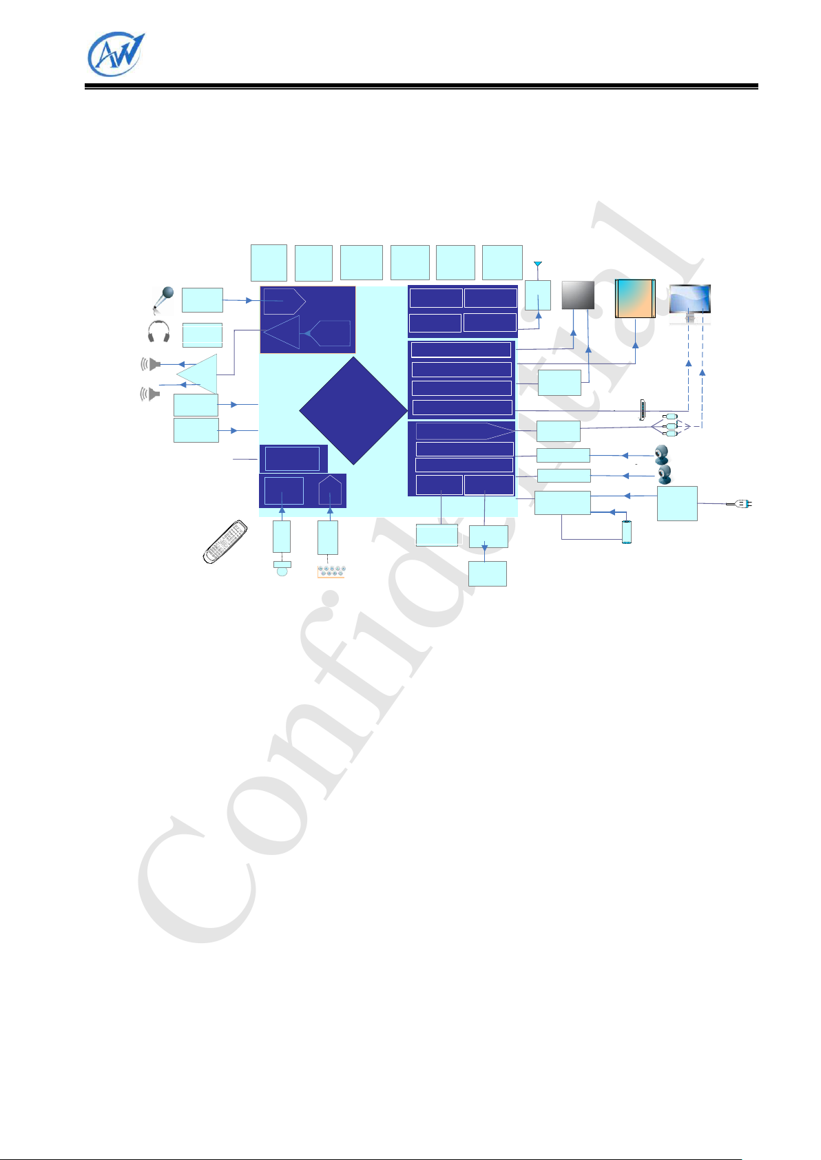
Video
HD Video
Display
LCD Display
&Touch
Head Phone
Microphone
Audio
Input
Audio
Output
AC
Adapter
Power
Management
PMU
System Power
Plug
Card
Slot0,1
DDR
DRAM
Nand
Flash
LCD
Buffer
HDMI
Port
Video Port0
CMOS Sensor0
TV-OUT
5V
AC Line
24M
Crystal
Battery
Support 4.1V/4.2V/4.36V
32.768K
Crystal
Class D
AMP
USB1,2
HOST
USB0
OGT
Audio
ADC
Audio
DAC
HP
AMP
Touch Controller
USB1,2
Controller
USB0
Controller
Video DAC
CSI0
G-Sensor
Key
IR
IR
Controller
ADC
WIFI
LVDS
Display
Security
Card
Slot2,3
Card
Controller2
3G
Card
Controller3
Card
Controller1
Card
Controller0
LVDS Controller
LCD Controller
HDMI Controller
CortexA8
GPU
VE
Processor
E-Mac
Cable
Line
CSI1
Video Port0
CMOS Sensor1
3. Functional Block Diagram
A10 Datasheet V1.21
Copyright © 2011-2012 Allwinner Technology. All Rights Reserved. 11
2012-04-06
Confidential
Allwinner Technology CO., Ltd. A10
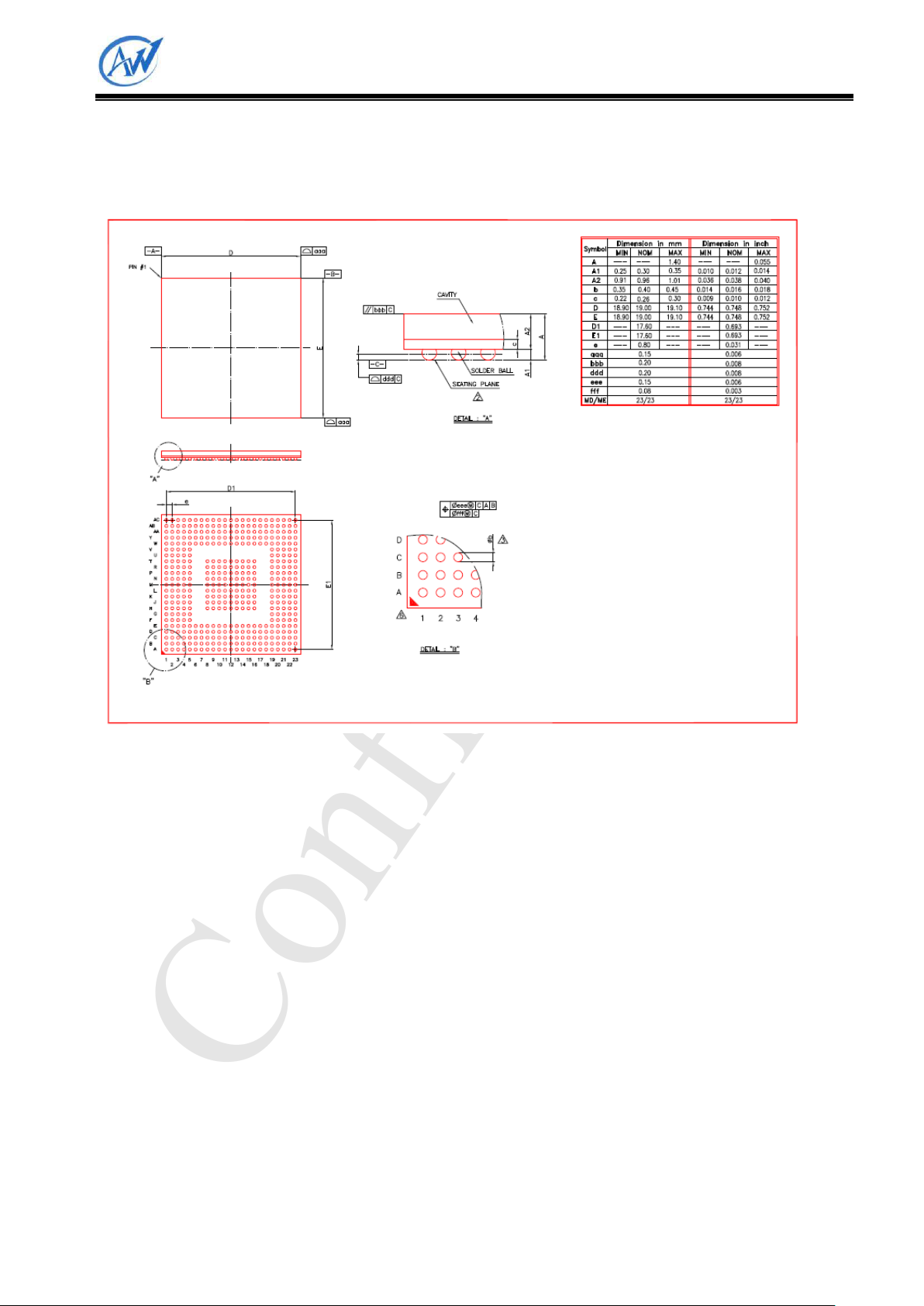
4. Pin Assignments
4.1. Dimension
Figure 4-1 A10 TFBGA441 Package Dimension
A10 Datasheet V1.21
Copyright © 2011-2012 Allwinner Technology. All Rights Reserved. 12
2012-04-06

Confidential
Allwinner Technology CO., Ltd. A10
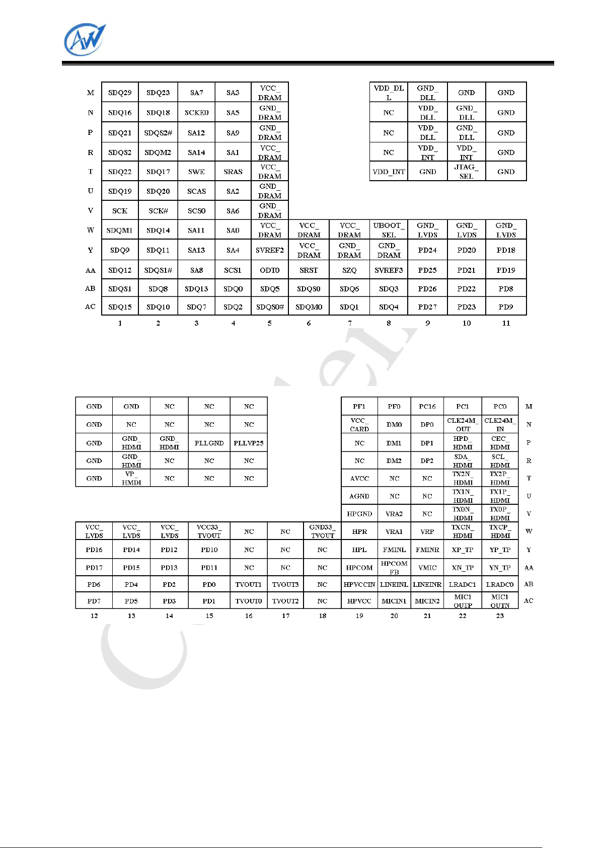
4.2. Pin Map
The following pin maps show the top view of the 441-pin FBGA package pin assignments in four
quadrants (A, B, C, D).
Figure 4-2 TFBGA441 Pin Map-Top View [Quadrant A]
Figure 4-3 TFBGA441 Pin Map-Top View [Quadrant B]
A10 Datasheet V1.21
Copyright © 2011-2012 Allwinner Technology. All Rights Reserved. 13
2012-04-06
Confidential
Allwinner Technology CO., Ltd. A10
Figure 4-4 TFBGA441 Pin Map-Top View [Quadrant C]
Figure 4-5 TFBGA441Pin Map-Top View [Quadrant D]
A10 Datasheet V1.21
Copyright © 2011-2012 Allwinner Technology. All Rights Reserved. 14
2012-04-06
Confidential
Allwinner Technology CO., Ltd. A10
BALL#
Pin Name
Function
Type
Reset
State
Pull
Up/Down
Buffer
Strength
(mA)
AB4
SDQ0
I/O
AC7
SDQ1
I/O
AC4
SDQ2
I/O
AB8
SDQ3
I/O
AC8
SDQ4
I/O
AB5
SDQ5
I/O
AB7
SDQ6
I/O
AC3
SDQ7
I/O
5. Pin Description
5.1. Pin Characteristics
1. BALL#: Ball numbers on the bottom side associated with each signals on the bottom.
2. Pin Name: Names of signals multiplexed on each ball (also notice that the name of the pin is the
signal name in function 0).
3. Function: Multiplexing function number.
Function 0 is the the default function, but is not necessarily the primary mode.
Functions 1 to 5 are possible modes for alternate functions.
4. Type: signal direction
- I = Input
- O = Output
- I/O = Input/Output
- A = Analog
- AIO = Analog Input/Output
- PWR = Power
- GND = Ground
5. Pin Reset State: The state of the terminal at reset (power up).
- 0: The buffer drives VOL(pull down/pull up resistor not activated)
- 0 (PD): The buffer drives VOL with an active pull down resistor.
- 1: The buffer drives VOH (pull down/pull up resistor not activated).
- 1 (PU): The buffer drives VOH with an active pull up resistor.
- Z: High-impedance
- L: High-impedance with an active pull down resistor.
- H: High-impedance with an active pull up resistor.
6. Pull Up/Down: Denotes the presence of an internal pull up or pull down resister. Pull up and pull
down resistor can be enabled or disabled via software.
7. Buffer Strength: Drive strength of the associated output buffer.
A10 Datasheet V1.21
Copyright © 2011-2012 Allwinner Technology. All Rights Reserved. 15
2012-04-06
Confidential
Allwinner Technology CO., Ltd. A10
BALL#
Pin Name
Function
Type
Reset
State
Pull
Up/Down
Buffer
Strength
(mA)
AB2
SDQ8
I/O
Y1
SDQ9
I/O
AC2
SDQ10
I/O
Y2
SDQ11
I/O
AA1
SDQ12
I/O
AB3
SDQ13
I/O
W2
SDQ14
I/O
AC1
SDQ15
I/O
N1
SDQ16
I/O
T2
SDQ17
I/O
N2
SDQ18
I/O
U1
SDQ19
I/O
U2
SDQ20
I/O
P1
SDQ21
I/O
T1
SDQ22
I/O
M2
SDQ23
I/O
L1
SDQ24
I/O
H1
SDQ25
I/O
L2
SDQ26
I/O
H2
SDQ27
I/O
J1
SDQ28
I/O
M1
SDQ29
I/O
G2
SDQ30
I/O
K2
SDQ31
I/O
H3
SVREF0
I
H4
SVREF1
I
Y5
SVREF2
I
AA8
SVREF3
I
AB6
SDQS0
I/O
AC5
SDQS0 #
O
W1
SDQM0
O
AB1
SDQS1
I/O
AA2
SDQS1 #
O
W1
SDQM1
O
R2
SDQM2
I/O
P2
SDQS2 #
O
H4
SVREF1
O
K1
SDQS3
I/O
J2
SDQS3 #
O
G1
SDQM3
O
A10 Datasheet V1.21
Copyright © 2011-2012 Allwinner Technology. All Rights Reserved. 16
2012-04-06
Confidential
Allwinner Technology CO., Ltd. A10
BALL#
Pin Name
Function
Type
Reset
State
Pull
Up/Down
Buffer
Strength
(mA)
V2
SCK#
O
V1
SCK
O
J4
SCKE1
O
N3
SCKE0
O W4
SA0
O
R4
SA1
O
U4
SA2
O
M4
SA3
O
Y4
SA4
O
N5
SA5
O
V4
SA6
O
M3
SA7
O
AA3
SA8
O
P4
SA9
O
L3
SA10
O
W3
SA11
O
P3
SA12
O
Y3
SA13
O
R3
SA14
O
K3
SBA0
O
L4
SBA1
O
K4
SBA2
O
T3
SWE
O
U3
SCAS
O
T4
SRAS
O
V3
SCS0
O
AA4
SCS1
O AA5
ODT0
O
J3
ODT1
O AA7
SZQ
AA6
SRST
O N8/P8/R8
NC
M8/N9/P9
VDD_DLL
P M9/N10/P10
GND_DLL
P
D5
PA0
0/1
I/O
ERXD3
2
SPI1_CS0
3
UART2_RTS
4
E5
PA1
0/1
I/O
ERXD2
2
A10 Datasheet V1.21
Copyright © 2011-2012 Allwinner Technology. All Rights Reserved. 17
2012-04-06

Confidential
Allwinner Technology CO., Ltd. A10
BALL#
Pin Name
Function
Type
Reset
State
Pull
Up/Down
Buffer
Strength
(mA)
SPI1_CLK
3
UART2_CTS
4
D6
PA2
0/1
I/O
ERXD1
2
SPI1_MOSI
3
UART2_TX
4
E6
PA3
0/1
I/O
ERXD0
2
SPI1_MISO
3
UART2_RX
4
D7
PA4
0/1
I/O
ETXD3
2
SPI1_CS1
3
E7
PA5
0/1
I/O
ETXD2
2
SPI3_CS0
3
D8
PA6
0/1
I/O
ETXD1
2
SPI3_CLK
3
E8
PA7
0/1
I/O
ETXD0
2
SPI3_MOSI
3
D9
PA8
0/1
I/O
ERXCK
2
SPI3_MISO
3
E9
PA9
0/1
I/O
ERXERR
2
SPI3_CS1
3
D10
PA10
0/1
I/O
ERXDV
2
UART1_TX
4
E10
PA11
0/1
I/O
EMDC
2
UART1_RX
4
D11
PA12
0/1
I/O
EMDIO
2
UART6_TX
3
UART1_RST
4
E11
PA13
0/1
I/O
ETXEN
2
A10 Datasheet V1.21
Copyright © 2011-2012 Allwinner Technology. All Rights Reserved. 18
2012-04-06

Confidential
Allwinner Technology CO., Ltd. A10
BALL#
Pin Name
Function
Type
Reset
State
Pull
Up/Down
Buffer
Strength
(mA)
UART6_RX
3
UART1_CTS
4
D12
PA14
0/1
I/O
ETXCK
2
UART7_TX
3
UART1_DTR
4
E12
PA15
0/1
I/O
ECRS
2
UART7_RX
3
UART1_DSR
4
D13
PA16
0/1
I/O
ECOL
2
CAN_TX
3
UART1_DCD
4
C13
PA17
0/1
I/O
ETXERR
2
CAN_RX
3
UART1_RING
4
A15
PB0
0/1
I/O
TWI0_SCK
2
B15
PB1
0/1
I/O
TWI0_SDA
2
A14
PB2
0/1
I/O
PWM0
2
B14
PB3
0/1
I/O
IR_TX
2
NC
3
EINT16
5
A13
PB4
0/1
I/O
IR_RX
2
B13
PB5
0/1
I/O
I2S_MCLK
2
AC97_MCLK
3
A12
PB6
0/1
I/O
I2S_BCLK
2
AC97_BCLK
3
B12
PB7
0/1
I/O
I2S_LRCK
2
AC97_SYNC
3
A11
PB8
0/1
I/O
A10 Datasheet V1.21
Copyright © 2011-2012 Allwinner Technology. All Rights Reserved. 19
2012-04-06

Confidential
Allwinner Technology CO., Ltd. A10
BALL#
Pin Name
Function
Type
Reset
State
Pull
Up/Down
Buffer
Strength
(mA)
I2S_DO0
2
AC97_DO
3
C12
PB9
0/1
I/O
I2S_DO1
2
C11
PB10
0/1
I/O
I2S_DO2
1
C10
PB11
0/1
I/O
I2S_DO3
1
C9
PB12
0/1
I/O
I2S_DI
2
AC97_DI
3
NC
4
B11
PB13
0/1
I/O
SPI2_CS1
2
NC
4
A10
PB14
0/1
I/O
SPI2_CS0
2
JTAG_MS0
3
B10
PB15
0/1
I/O
SPI2_CLK
2
JTAG_CK0
3
A9
PB16
0/1
I/O
SPI2_MOSI
2
JTAG_DO0
3
B9
PB17
0/1
I/O
SPI2_MOSO
2
JTAG_DI0
3
A8
PB18
0/1
I/O
TWI1_SCK
2
B8
PB19
0/1
I/O
TWI1_SDA
2
C8
PB20
0/1
I/O
TWI2_SCK
2
C7
PB21
0/1
I/O
TWI2_SDA
2
A7
PB22
0/1
I/O
UART0_TX
2
IR1_TX
3
B7
PB23
0/1
I/O
UART0_RX
2
A10 Datasheet V1.21
Copyright © 2011-2012 Allwinner Technology. All Rights Reserved. 20
2012-04-06

Confidential
Allwinner Technology CO., Ltd. A10
BALL#
Pin Name
Function
Type
Reset
State
Pull
Up/Down
Buffer
Strength
(mA)
IR1_RX
3
M23
PC0
0/1
I/O
NWE#
2
SPI0_MOSI
3
M22
PC1
0/1
I/O
NALE
2
SPI0_MISO
3
L23
PC2
0/1
I/O
NCLE
2
SPI0_CLK
3
L22
PC3
0/1
I/O
Pull Up
(default)
NCE1
2
SDC1_CMD
3
K23
PC4
0/1
I/O
Pull Up
(default)
NCE0
1
K22
PC5
0/1
I/O
NRD
1
SDC1_CLK
2
J23
PC6
0/1
I/O
Pull Up
(default)
NRB0
2
SDC2_CMD
3
J22
PC7
0/1
I/O
Pull Up
(default)
NRB1
2
SDC2_CLK
3
H23
PC8
0/1
I/O
ND0
2
SDC2_D0
3
H22
PC9
0/1
I/O
ND1
2
SDC2_D1
3
G23
PC10
0/1
I/O
ND2
2
SDC2_D2
3
G22
PC11
0/1
I/O
ND3
2
SDC2_D3
3
H21
PC12
0/1
I/O
ND4
2
SDC1_D0
3
H20
PC13
0/1
I/O
A10 Datasheet V1.21
Copyright © 2011-2012 Allwinner Technology. All Rights Reserved. 21
2012-04-06

Confidential
Allwinner Technology CO., Ltd. A10
BALL#
Pin Name
Function
Type
Reset
State
Pull
Up/Down
Buffer
Strength
(mA)
ND5
2
SDC1_D1
3
G21
PC14
0/1
I/O
ND6
2
SDC1_D2
3
G20
PC15
0/1
I/O
ND7
2
SDC1_D3
3
M21
PC16
0/1
I/O
Pull Down
(default)
NWP
1
F23
PC17
0/1
I/O
Pull Up
(default)
NCE2
1
F22
PC18
0/1
I/O
Pull Up
(default)
NCE3
1
L21
PC19
0/1
I/O
NCE4
1
SPI2_CS0
2
EINT12
5
K21
PC20
0/1
I/O
NCE5
1
SPI2_CLK
2
EINT13
5
J21
PC21
0/1
I/O
NCE6
1
SPI2_MOSI
2
EINT14
5
J20
PC22
0/1
I/O
NCE7
1
SPI2_MISO
2
EINT15
5
G19
PC23
0/1
I/O
Pull Up
(default)
SPI0_CS0
2
F21
PC24
0/1
I/O
NDQS
AB15
PD0
0/1
I/O
LCD0_D0
2
LVDS0_VP0
3
AC15
PD1
0/1
I/O
LCD0_D1
2
LVDS0_VN0
3
A10 Datasheet V1.21
Copyright © 2011-2012 Allwinner Technology. All Rights Reserved. 22
2012-04-06

Confidential
Allwinner Technology CO., Ltd. A10
BALL#
Pin Name
Function
Type
Reset
State
Pull
Up/Down
Buffer
Strength
(mA)
AB14
PD2
0/1
I/O
LCD0_D2
2
LVDS0_VP1
3
AC14
PD3
0/1
I/O
LCD0_D3
2
LVDS0_VN1
3
AB13
PD4
0/1
I/O
LCD0_D4
2
LVDS0_VP2
3
AC13
PD5
0/1
I/O
LCD0_D5
2
LVDS0_VN2
3
AB12
PD6
0/1
I/O
LCD0_D6
2
LVDS0_VPC
3
AC12
PD7
0/1
I/O
LCD0_D7
2
LVDS0_VNC
3
AB11
PD8
0/1
I/O
LCD0_D8
2
LVDS0_VP3
3
AC11
PD9
0/1
I/O
LCD0_D9
2
LVDS0_VN3
3
Y15
PD10
0/1
I/O
LCD0_D10
2
LVDS1_VP0
3
AA15
PD11
0/1
I/O
LCD0_D11
2
LVDS1_VN0
3
Y14
PD12
0/1
I/O
LCD0_D12
2
LVDS1_VP1
3
AA14
PD13
0/1
I/O
LCD0_D13
2
LVDS1_VN1
3
Y13
PD14
0/1
I/O
LCD0_D14
2
LVDS1_VP2
3
AA13
PD15
0/1
I/O
A10 Datasheet V1.21
Copyright © 2011-2012 Allwinner Technology. All Rights Reserved. 23
2012-04-06

Confidential
Allwinner Technology CO., Ltd. A10
BALL#
Pin Name
Function
Type
Reset
State
Pull
Up/Down
Buffer
Strength
(mA)
LCD0_D15
2
LVDS1_VN2
3
Y12
PD16
0/1
I/O
LCD0_D16
2
LVDS1_VPC
3
AA12
PD17
0/1
I/O
LCD0_D17
2
LVDS1_VNC
3
Y11
PD18
0/1
I/O
LCD0_D18
2
LVDS1_VP3
3
AA11
PD19
0/1
I/O
LCD0_D19
2
LVDS1_VN3
3
Y10
PD20
0/1
I/O
LCD0_D20
2
CSI1_MCLK
3
AA10
PD21
0/1
I/O
LCD0_D21
2
SMC_VPPEN
3
AB10
PD22
0/1
I/O
LCD0_D22
2
SMC_VPPPP
3
AC10
PD23
0/1
I/O
LCD0_D23
2
SMC_DET
3
Y9
PD24
0/1
I/O
LCD0_CLK
2
SMC_VCCEN
3
AA9
PD25
0/1
I/O
LCD0_DE
2
SMC_RST
3
AB9
PD26
0/1
I/O
LCD0_HSYNC
2
SMC_SLK
3
AC9
PD27
0/1
I/O
LCD0_VSYNC
2
SMC_SDA
3
E23
PE0
0/1
I/O
TS0_CLK
2
A10 Datasheet V1.21
Copyright © 2011-2012 Allwinner Technology. All Rights Reserved. 24
2012-04-06
Confidential
Allwinner Technology CO., Ltd. A10
BALL#
Pin Name
Function
Type
Reset
State
Pull
Up/Down
Buffer
Strength
(mA)
CSI0_PCK
3
E22
PE1
0/1
I/O
TS0_ERR
2
CSI0_CK
3
D23
PE2
0/1
I/O
TS0_SYNC
2
CSI0_HSYNC
3
D22
PE3
0/1
I/O
TS0_DVLD
2
CSI0_VSYNC
3
C23
PE4
0/1
I/O
TS0_D0
2
CSI0_D0
3
C22
PE5
0/1
I/O
TS0_D1
2
CSI0_D1
3
B23
PE6
0/1
I/O
TS0_D2
2
CSI0_D2
3
B22
PE7
0/1
I/O
TS0_D3
2
CSI0_D3
3
A23
PE8
0/1
I/O
TS0_D4
2
CSI0_D4
3
A22
PE9
0/1
I/O
TS0_D5
2
CSI0_D5
3
B21
PE10
0/1
I/O
TS0_D6
2
CSI0_D6
3
A21
PE11
0/1
I/O
TS0_D7
2
CSI0_D7
3
M20
PF0
0/1
I/O
SDC0_D1
2
JTAG_MS1
4
M19
PF1
0/1
I/O
SDC0_D0
2
JTAG_DI1
4
A10 Datasheet V1.21
Copyright © 2011-2012 Allwinner Technology. All Rights Reserved. 25
2012-04-06
 Loading...