

Alliance Semiconductor Corporation AS6UA25616-TI, AS6UA25616-TC, AS6UA25616-BI, AS6UA25616-BC Datasheet

October 2000
2.3V to 3.6V 256K×16 Intelliwatt™ low-power CMOS SRAM with one chip enable
AS6UA25616
®
‘Features
• AS6UA25616
• Intelliwatt™ active power circuitry
• Industrial and c o mmercial temperature r anges availab le
• Organization: 262,144 words x 16 bits
• 2.7V to 3.6 V at 55 ns
• 2.3V to 2.7 V at 70 ns
• Low power consumption: ACTIVE
- 114 mW at 3.6V and 55 ns
- 68 mW at 2.7V and 70 ns
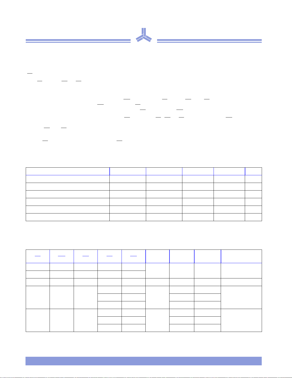
Logic block diagram
A0
A1
I/O9–I/O16
WE
UB
OE
LB
CS
A12
A13
I/O1–I/O8
A2
A3
A4
A6
A7
A8
Row Decoder
I/O
buffer
256K × 16
Array
(4,194,304)
Control circuit
Column decoder
A5
A9
A10
A11
A14
A15
A16
A17
• Low power consumption: STANDBY
- 72 µW max at 3.6V
W max at 2.7V
µ
- 41
• 1.2V data retention
• Equal access and cycle times
• Easy memory expansion with CS
, OE inputs
• Smallest footprint packages
- 48-ball FBGA
- 400-mil 44-pin TSOP II
• ESD protection ≥ 2000 volts
• Latch - u p cur r en t ≥ 200 mA
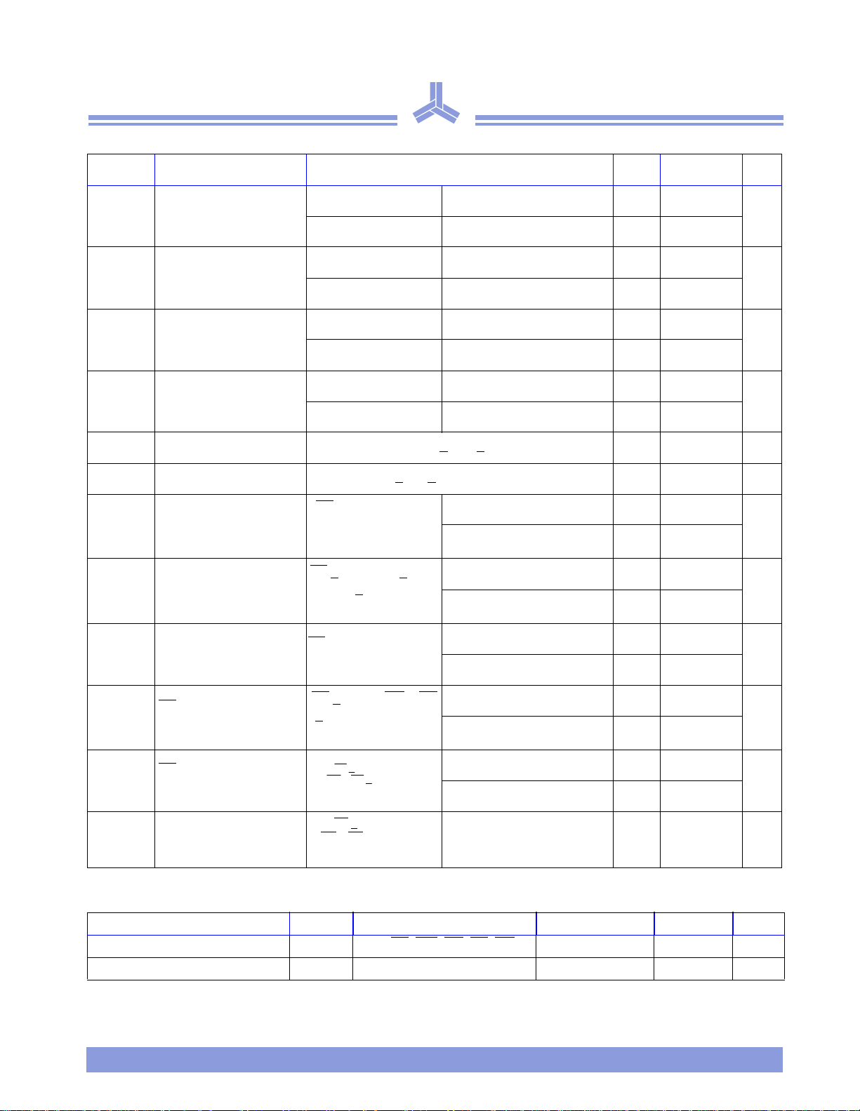
Pin arrangement (top view)
44-pin 400-mil TSOP II
V
CC
I/O1
I/O2
I/O3
I/O4
V
V
I/O5
I/O6
I/O7
I/O
WE
A17
A16
A15
A14
A13
A2
A0
CS
CC
8
SS
V
SS
1A4
2A3
3
4A1
5
6
7
8
9
10
11
12
13
14
15
16
17
1
19
20
21
22
44
A5
A6
43
A7
42
OE
41
UB
40
39
LB
I/O16
38
I/O15
37
I/O14
36
I/O13
35
V
34
33
32
31
30
29
28
8
27
26
25
24
23
SS
V
CC
I/O12
I/O11
I/O10
I/O9
NC
A8
A9
A10
A11
A12
48-CSP Ball-Grid-Array Package
123456
ALB
BI/O9UB
OE A0 A1 A2 NC
A3 A4 CS I/O1
C I/O10 I/O11 A5 A6 I/O2 I/O3
DV
I/O12 A17 A7 I/O4 V
SS
EVCCI/O13 NC A16 I/O5 V
F I/O15 I/O14 A14 A15 I/O6 I/O7
G I/O16 NC A12 A13 WE
HNCA8A9A10A11NC
Selection guide
V
Range
CC
Operating (I
Max (mA) Max (
Product
Min
(V)
Typ
(V)
2
Max
(V)
Speed
(ns)
AS6UA25616 2.7 3.0 3.6 55 2 20
AS6UA25616 2.3 2.5 2.7 70 1 15
10/6/00 ALLIANCE SEMICONDUCTOR 1
Power Dissipation
) Standby (I
CC
Copyright ©2000 Alliance Semiconductor. All rights reserved.
CC
SS
I/O8
A)
µ
SB1
)
AS6UA25616
®
Functional description
The AS6U A256 16 is a low -po wer CMOS 4,194, 3 04-bi t Stat ic Random Acce ss Memory (SRAM) de vi ce org an ized as 262 ,1 44 wor ds x 16
bits. It is designed for memory applications where slow data access, low power, and simple interfacing are desired.
Equal address access and cycle times (t
(CS
) permit easy memory expansion with multiple-bank memory systems.
When CS
consumption at 3.6V and 55 ns; 41µW at 2.7V and 70 ns. The device also returns data when V
consumption.
A write cycle is accomplished by asserting write enable (WE
I/O1–O16 is written on the rising edge of WE
I/O pins only after outputs have been disabled with output enable (OE
A read cycle is accomplished by asserting output enable (OE
drives I/O pins with the data word referenced by the input address. When either chip enable or output enable is inactive, or write enable is
active, o r (UB
These device s provide mu l tiple center po wer and ground pins, and separate byte enable controls, allowing individual bytes to be written
and read. LB
All chip inputs and outputs are CMOS-compatible, and operation is from a single 2.3V to 3.6V supply. Device is available in the JEDEC
standard 400-mm, TSOP II, and 48-ball FBGA packages.
is high, or UB and LB are high, the device enters standby mode: the AS6UA25616 is guaranteed not to exceed 72 µW power
) and (LB), output drivers stay in high-impedance mode.
controls the lowe r bits, I/O1–I/O8, and UB controls the high er bits , I /O 9 –I/O16.
, tRC, tWC) of 55 /70 ns are ideal fo r low-pow er a p plicat io ns. Ac tiv e h igh and low chip en ables
AA
is reduc ed to 1.5V for even lower pow er
CC
) an d ch ip en able (CS) low, and UB and/or LB low. Data on the input pins
(write cycle 1) or CS (write cycle 2). To avoid bus contentio n, external device s should drive
) or write enable (WE).
), chip enable (CS), UB and LB low, with write enable (WE) high. The chip
Absolute m aximum ratings
Parameter Device Symbol Min Max Unit
Voltage on V
Voltage on any I/O pin relative to GND V
Power dissipation P
Storage temp erature (plastic) T
Tempe rature wi th V
DC output current (low) I
Note: Stresse s greater than th ose listed under A bsolute Maximu m Ratings may cause permanent damage to the device. This is a stress rating only and
functional operation of the device at these or any other conditions outside those indicated in the operational sections of this specification is not implied.
Exposure to absolute maximum rating conditions for extended periods may affect reliability.
relative to V
CC
CC
SS
applied T
V
tI/O
bias
OUT
tIN
D
stg
–0.5 V
+ 0.5 V
CC
–0.5 V
–1.0W
–65 +150
–55 +125
o
C
o
C
–20mA
Truth table
Supply
CS
WE OE LB UB
HXXXX
LXXHH
LHHXXI
LH
LHL
LL D
LH
LLX
LL DIND
Key: X = Don’t care, L = Low, H = High.
Current I/O1–I/O8 I/O9–I/O16 Mode
I
SB
CC
I
CC
I
CC
High Z High Z Standby (ISB)
High Z High Z Output disable (ICC)
D
OUT
OUT
D
IN
High Z
OUT
D
OUT
High Z
IN
IN
Read (I
Write (I
CC
CC
)H L High Z D
)H L High Z D
2 ALLIANCE SEMICONDUCTOR 10/6/00
AS6UA25616
®
Recommended operating condition (over the operating range)
Parameter Description Test Conditions Min Max Unit
= –2.1mA VCC = 2.7V 2.4
I
V
OH
V
OL
V
IH
V
IL
Output HIGH Voltage
Output LOW Voltage
Input HIGH Voltage
Input LOW Voltage
OH
I
= –0.5mA VCC = 2.3V 2.0
OH
I
= 2.1mA VCC = 2.7V 0.4
OL
= 0.5mA VCC = 2.3V 0.4
I
OL
V
= 2.7V 2.2 VCC + 0.5
CC
V
= 2.3V 2.0 VCC + 0.3
CC
V
= 2.7V –0.5 0.8
CC
= 2.3V –0.3 0.6
V
CC
V
V
V
V
I
IX
I
OZ
I
CC
I
@
CC1
1MHz
I
CC2
I
SB
I
SB1
I
SBDR
Input Load Current GND < VIN < V
Output Load Current GND < VO < V
CS
VCC Operating Supply
Current
Av er age VCC Operating
Supply Current at 1 MHz
Av er age VCC Operating
Supply Current
CS Power Down Current;
TTL Inputs
CS Power Down Current;
CMOS Inputs
Data Rete ntion
= VIL, VIN = VIL
or V
IH, IOUT
= 0mA,
f = 0
CS
< 0.2V, V
or V
IN
> VCC – 0.2V,
IN
< 0.2V
f = 1 mS
CS ≠ VIL, VIN = VIL or
V
, f = f
IH
CS
> VIH or UB = LB
>
VIH, other inputs =
V
or VIH, f = 0
IL
CS > VCC – 0.2V or
UB
= LB > VCC – 0.2V,
other i nputs = 0V – V
CS > VCC – 0.1V,
UB
= LB = VCC – 0.1V
f = 0
Max
CC
, f = f
CC;
Max
CC
–1 +1
Outputs High Z –1 +1
= 3.6V 2
V
CC
= 2.7V 1
V
CC
= 3.6V 5
V
CC
= 2.7V 4
V
CC
V
= 3.6V (55/70 ns) 40/30
CC
V
= 2.7V (70 ns) 25
CC
= 3.6V 100
V
CC
= 2.7V 100
V
CC
VCC = 3.6V 20
= 2.7V 15
V
CC
VCC = 1.2V 2
A
µ
A
µ
mA
mA
mA
A
µ
A
µ
A
µ
Capacitance (f = 1 MHz, Ta = Room temperature, VCC = NOMINAL)2
Parameter Symbol Signals Test conditions Max Unit
Input capacitance C
I/O capacitance C
10/6/00 ALLIANCE SEMICONDUCTOR 3
IN
I/O
A, CS, WE, OE, LB, UB VIN = 0V 5 pF
I/O VIN = V
= 0V 7 pF
OUT
 Loading...