

Page 1

Allen-Bradley
FLEX I/O
PROFIBUS
User
Adapter
(Cat. No. 1794-APB)
Manual
–2
Page 2

Important User Information
Solid state equipment has operational characteristics differing from
those of electromechanical equipment. “Safety Guidelines for the
Application, Installation and Maintenance of Solid State Controls”
(Publication SGI-1.1) describes some important dif
ferences between
solid state equipment and hard–wired electromechanical devices.
Because of this difference, and also because of the wide variety of
uses for solid state equipment, all persons responsible for applying
this equipment must satisfy themselves that each intended
application of this equipment is acceptable.
In no event will the Allen-Bradley Company be responsible or liable
for indirect or consequential damages resulting from the use or
application of this equipment.
The examples and diagrams in this manual are included solely for
illustrative purposes. Because of the many variables and
requirements associated with any particular installation, the
Allen-Bradley Company cannot assume responsibility or liability for
actual use based on the examples and diagrams.
No patent liability is assumed by Allen-Bradley Company with
respect to use of information, circuits, equipment, or software
described in this manual.
Reproduction of the contents of this manual, in whole or in part,
without written permission of the Allen-Bradley Company is
prohibited.
Throughout this manual we use notes to make you aware of safety
considerations.
ATTENTION: Identifies information about practices
or circumstances that can lead to personal injury or
!
death, property damage, or economic loss.
Attentions help you:
• identify a hazard
• avoid the hazard
• recognize the consequences
Important: Identifies information that is especially important for
successful application and understanding of the product.
Microsoft is a registered trademark of the Microsoft Corporation.
Windows is a trademark of the Microsoft Corporation.
FLEX I/O and PLC-5 are trademarks of the Allen-Bradley Company
PROFIBUS is a trademark of the PROFIBUS User Organization
, Inc.
Page 3

About this User Manual
Preface
Purpose
Vocabulary
this Manual Contains
What
Use this manual to install and configure your FLEX I/O
TM
PROFIBUS Adapter, cat. no. 1794-APB.
In this manual, we refer to:
• the FLEX I/O PROFIBUS adapter module as the “adapter”
• the programmable controller as the “processor”
The following table shows what each chapter of this manual
describes:
Chapter Title Describes
Overview of FLEX I/O
1
2
3
and Your PROFIBUS
Adapter
How Communication
Takes Place and I/O
Mapping
Connect the Adapter to
the PROFIBUS DP
Network
The FLEX I/O system and PROFIBUS
adapter.
Backplane communication between the
modules and the adapter, and how data is
mapped into the image table.
The DP physical layer, how to select the line
type you should use and how to connect to
and terminate the network.
Configure the Adapter for
4
5 Troubleshooting
Appendix A Specifications Adapter specifications.
Appendix B Device Data Base File Device Data Base (GSD) File.
Master/Slave
Communication
How to configure the adapter for
master/slave communication.
How to use the indicators for
troubleshooting.
Publication 1794-6.5.6 – April 1996
Page 4

About this User ManualP –2
g
Catalog
D
Related Publications
For additional information on planning and installing your
PROFIBUS system using FLEX I/O modules, refer to the following
publications:
Catalo
Number
1794-APB 24V dc PROFIBUS Adapter Installation Instructions 1794-5.40
1794-TB2
1794-TB3
1794-TBN Terminal Base Unit Installation Instructions 1794-5.16
1794-TBNF Fused Terminal Base Unit Installation Instructions 1794-5.17
1794-PS1 Power Supply Installation Instructions 1794-5.35
1794-IB16 24V dc 16 Input Module Installation Instructions 1794-5.4
1794-OB16 24V dc 16 Output Module Installation Instructions 1794-5.3
1794-IR8 24V dc RTD Analog 8 Input Module Installation Instructions
1794-IT8 24V dc Thermocouple Analog 8 Input
1794-IE8 24V dc Selectable Analog 8 Input
1794-OE4 24V dc Selectable Analog 4 Output
1794-IE4XOE2 24V dc 4 Input/2 Output Analog Combo
1794-IB8S 24V dc Sensor Input Module Installation Instructions 1794-5.7
1794-IA8 120V ac 8 Input Module Installation Instructions 1794-5.9
1794-OA8 120V ac 8 Output Module Installation Instructions 1794-5.10
1794-OW8 24V dc 8 Relay Output Module Installation Instructions 1794-5.19
1794-CE1 Extender Cable Installation Instructions 1794-5.12
1794-NM1 Mounting Kit Installation Instructions 1794-5.13
s
escription
2-wire Terminal Base
3-wire Terminal Base
Module
Module
Module
Module
Installation Instructions 1794-5.2
Installation Instructions
Installation Instructions
Installation Instructions
Installation Instructions
Related Publications
Pub. Type Pub. Number
1794-5.22
User Manual
User Manual
User Manual
User Manual
User Manual
1794-6.5.4
1794-5.21
1794-6.5.7
1794-5.6
1794-6.5.2
1794-5.5
1794-6.5.2
1794-5.15
1794-6.5.2
Conventions
Publication 1794-6.5.6 – April 1996
More
Information...
To order these publications, contact your local Allen-Bradley
representative.
This icon appears when more information is available in related
documentation.
Page 5

About this User Manual P –3
Compliance
to
European Union Directives
If this product has the CE mark it is approved for installation within
the European Union and EEA regions. It has been designed and
tested to meet the following directives.
EMC Directive
This product is tested to meet Council Directive 89/336/EEC
Electromagnetic Compatibility (EMC) and the following standards,
in whole or in part, documented in a technical construction file:
• EN 50081-2EMC – Generic Emission Standard, Part 2 –
Industrial Environment
• EN 50082-2EMC – Generic Immunity Standard, Part 2 –
Industrial Environment
This product is intended for use in an industrial environment.
Low V
oltage Directive
This product is tested to meet Council Directive 73/23/EEC
Low Voltage, by applying the safety requirements of EN 61131–2
Programmable Controllers, Part 2 – Equipment Requirements and
Tests.
For specific information required by EN 61131-2, see the appropriate
sections in this publication, as well as the following Allen-Bradley
publications:
• Industrial Automation Wiring and Grounding Guidelines For
Noise Immunity, publication 1770-4.1
• Guidelines for Handling Lithium Batteries, publication AG-5.4
• Automation Systems Catalog, publication B111
Publication 1794-6.5.6 – April 1996
Page 6

About this User ManualP –4
Publication 1794-6.5.6 – April 1996
Page 7

Table of Contents
Overview
Y
our PROFIBUS Adapter
of FLEX I/O and
Module
How Communication T
Place and I/O Image
Table Mapping
akes
Chapter
1
What
this Chapter Contains
FLEX I/O System
The
and Remove your System Easily
Mount
Optional Accessories 1–2. . . . . . . . . . . . . . . . . . . . . . . . . . . . . . . . . .
Mounting Kit (1794-NM1) 1–3. . . . . . . . . . . . . . . . . . . . . . . . . . . . .
Purpose
PROFIBUS Adapter Components 1–6. . . . . . . . . . . . . . . . . . . . . . . . .
of the 1794-APB FLEX I/O Adapter
Diagnostic Indicators 1–6. . . . . . . . . . . . . . . . . . . . . . . . . . . . . . . .
Network Connector 1–7. . . . . . . . . . . . . . . . . . . . . . . . . . . . . . . . .
Setting the Node Address Switches 1–7. . . . . . . . . . . . . . . . . . . . . .
Wiring
Power
Chapter 2
What
this Chapter Contains
Communication
I/O Structure
Polled
Adapter
Mapping
1794-IB16
T
able Mapping
1794-IB16
1794-OB16
T
able Mapping
1794-OB16
1794-IB8S
T
able Mapping
1794-IB8S
1794-IA8
T
able Mapping
1794-IA8
1794-OA8
T
able Mapping
1794-OA8
1794-OW8
Image T
1794-OW8
1794-IE8
1794-IE8
1794-IE8
1794-IE8
1794-OE4
Over the I/O Backplane
Input Status W
Data into the Image T
– 16-point Discrete Input Module Image
Memory Map
– 16-point Discrete Output Module Image
Memory Map
– 8-point Discrete Sensor Input Module Image
Memory Map
– 8-point Discrete Input Module Image
Memory Map
– 8-point Discrete Output Module Image
Memory Map
– 8-point Discrete Relay Output Module
able Mapping
Memory Map
– 8 Input Analog Module
Memory Map
Range Selection Bits
W
ord/Bit Descriptions 2–10. . . . . . . . . . . . . . . . . . . . . . .
– 4 Output Analog Module Image T
ord 2–3. . . . . . . . . . . . . . . . . . . . . . . . . . . .
able 2–4. . . . . . . . . . . . . . . . . . . . . . . .
able Mapping
1–1. . . . . . . . . . . . . . . . . . . . . . . . . . . . .
1–1. . . . . . . . . . . . . . . . . . . . . . . . . . . . . . . . .
1–2. . . . . . . . . . . . . . . . . . . . .
1–5. . . . . . . . . . . . . . . . .
1–7. . . . . . . . . . . . . . . . . . . . . . . . . . . . . . . . . . . . . .
2–1. . . . . . . . . . . . . . . . . . . . . . . . . . . . .
2–1. . . . . . . . . . . . . . . . . . . .
2–2. . . . . . . . . . . . . . . . . . . . . . . . . . . . . . . . . . .
2–4. . . . . . . . . . . . . . . . . . . . . . . . . . . . . . . . . .
2–4. . . . . . . . . . . . . . . . . . . . . . . . . . . .
2–5. . . . . . . . . . . . . . . . . . . . . . . . . . . . . . . . . .
2–5. . . . . . . . . . . . . . . . . . . . . . . . . . .
2–6. . . . . . . . . . . . . . . . . . . . . . . . . . . . . . . . . .
2–6. . . . . . . . . . . . . . . . . . . . . . . . . . . .
2–7. . . . . . . . . . . . . . . . . . . . . . . . . . . . . . . . . .
2–7. . . . . . . . . . . . . . . . . . . . . . . . . . . . .
2–7. . . . . . . . . . . . . . . . . . . . . . . . . . . . . . . . . .
2–8. . . . . . . . . . . . . . . . . . . . . . . . . . . .
2–8. . . . . . . . . . . . . . . . . . . . . . . . . . . . .
2–8. . . . . . . . . . . . . . . . . . . . . . . . . . .
2–9. . . . . . . . . . . . . . . . . . . . . .
2–9. . . . . . . . . . . . . . . . . . . . . . . . . . . . .
2–10. . . . . . . . . . . . . . . . . . . . . . .
2–11. . . .
Page 8

Table of Contents–2
Connect the Adapter to
the PROFIBUS DP Network
1794-OE4
1794-OE4
1794-OE4
1794-IE4XOE2
1794-IE4XOE2
1794-IE4XOE2
1794-IE4XOE2
1794-IR8
1794-IR8
1794-IR8
1794-IR8
1794-IT8
1794-IT8
1794-IT8
1794-IT8
Chapter
What
this Chapter Contains
Cables 3–2. . . . . . . . . . . . . . . . . . . . . . . . . . . . . . . . . . . . . . . .
T-junction Connectors 3–2. . . . . . . . . . . . . . . . . . . . . . . . . . . . .
Termination Blocks 3–2. . . . . . . . . . . . . . . . . . . . . . . . . . . . . . . .
Bus Connector 3–2. . . . . . . . . . . . . . . . . . . . . . . . . . . . . . . . . .
Cables 3–3. . . . . . . . . . . . . . . . . . . . . . . . . . . . . . . . . . . . . . . .
T-junction Connectors 3–3. . . . . . . . . . . . . . . . . . . . . . . . . . . . .
Termination Blocks 3–3. . . . . . . . . . . . . . . . . . . . . . . . . . . . . . . .
Bus Connector 3–3. . . . . . . . . . . . . . . . . . . . . . . . . . . . . . . . . .
Connect
Connect
Terminate
Terminate
Terminate
Memory Map
Range Selection Bits (W
W
ord/Bit Descriptions 2–12. . . . . . . . . . . . . . . . . . . . . .
– Analog Combo Module Image T
Memory Map
Range Selection Bits
W
ord/Bit Descriptions 2–15. . . . . . . . . . . . . . . . . .
– R
TD Input Analog Module Image T
Read
W
rite 2–17. . . . . . . . . . . . . . . . . . . . . . . . . . . . . . . . . . . .
W
ord/Bit Descriptions 2–17. . . . . . . . . . . . . . . . . . . . . .
– Thermocouple Input Module Image T
Read
W
rite 2–21. . . . . . . . . . . . . . . . . . . . . . . . . . . . . . . . . . .
W
ord/Bit Descriptions 2–21. . . . . . . . . . . . . . . . . . . . . . .
rite W
ord 6) 2–12. . . . . . . . . . .
able Mapping
able Mapping
able Mapping
3
the Adapter to the Network
to the Adapter
the Network
at the Adapter Using Line A
at the Adapter Using Line B
2–12. . . . . . . . . . . . . . . . . . . . . . . . . . . .
2–14. .
2–14. . . . . . . . . . . . . . . . . . . . . . . .
2–15. . . . . . . . . . . . . . . . . . .
2–16. . . .
2–17. . . . . . . . . . . . . . . . . . . . . . . . . . . . . . . . . .
2–20. .
2–20. . . . . . . . . . . . . . . . . . . . . . . . . . . . . . . . . .
3–1. . . . . . . . . . . . . . . . . . . . . . . . . . . . .
3–4. . . . . . . . . . . . . . . . . . . . . . .
3–5. . . . . . . . . . . . . . . . . . . . . . . . . . . . . .
3–6. . . . . . . . . . . . . . . . . . . . . . . . . . . . . . . . .
3–6. . . . . . . . . . . . . . . . . . . .
3–6. . . . . . . . . . . . . . . . . . . .
Configure the Adapter for
Master/Slave Communication
Chapter 4
What
this Chapter Contains
Master/Slave Communication T
How
Entering Send Parameter Data 4–2. . . . . . . . . . . . . . . . . . . . . . . . . . .
Parameter Data
User
Entering
Read
Check Configuration Data
Configuration Response Data
akes Place 4–1. . . . . . . . . . . . . . .
4–1. . . . . . . . . . . . . . . . . . . . . . . . . . . . .
4–2. . . . . . . . . . . . . . . . . . . . . . . . . . . . . . . .
4–6. . . . . . . . . . . . . . . . . . . . . . . .
4–9. . . . . . . . . . . . . . . . . . . . . . .
Page 9

Table of Contents–3
Troubleshooting
Specifications
Device Data Base File
Glossary
Chapter
5
What
this Chapter Contains
Troubleshooting
Viewing
Status from the Master’s Configuration Software
with the Indicators
Appendix A
Specifications
. . . . . . . . . . . . . . . . . . . . . . . . . . . . . . . . . . . . . . .
Appendix B
Device
Data Base File
. . . . . . . . . . . . . . . . . . . . . . . . . . . . . . . . .
Glossary
. . . . . . . . . . . . . . . . . . . . . . . . . . . . . . . . . . . . . . . . . . . . . . . . . .
5–1. . . . . . . . . . . . . . . . . . . . . . . . . . . . .
5–1. . . . . . . . . . . . . . . . . . . . . . . .
5–2. . . . . . . .
A–1
B–1
G–1
Page 10
Chapter 1
Overview of FLEX I/O and Your
PROFIBUS Adapter Module
What
this Chapter Contains
The FLEX I/O System
Adapter
This chapter describes:
• what the FLEX I/O system is and what it contains
• how to mount and remove your system easily
• optional accessories
• mounting dimensions and spacing requirements
• the 1794-APB FLEX I/O PROFIBUS Adapter
• adapter components
• how to connect power wiring
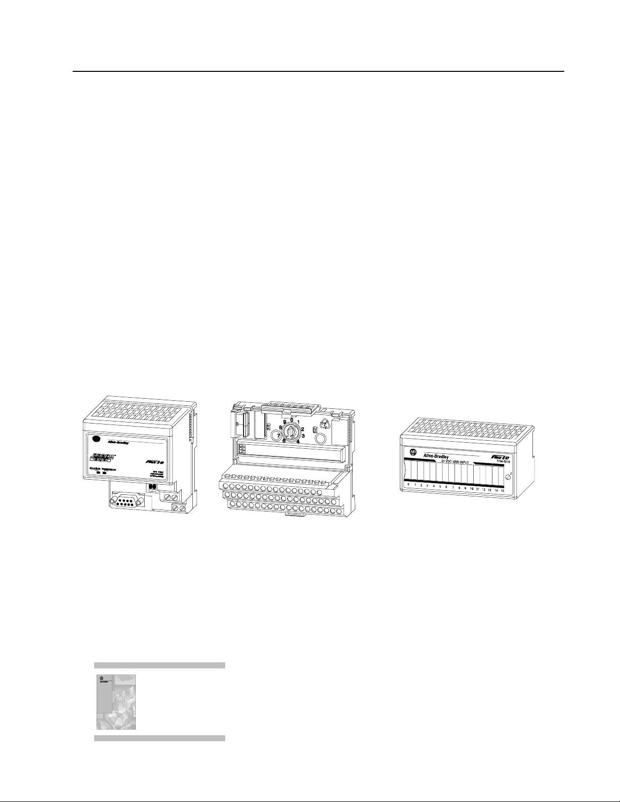
FLEX I/O is a small, modular I/O system for distributed
applications that performs all of the functions of rack-based I/O. The
FLEX I/O system contains the following components:
Terminal Base
I/O Module
More
Information...
20125
• PROFIBUS adapter/power supply – powers the internal logic for
as many as eight I/O modules
• terminal base – contains a terminal strip to terminate wiring for
two- or three-wire devices
• I/O module – contains the bus interface and circuitry needed to
perform specific functions related to your application
For information on how communication occurs over the FLEX I/O
system backplane, refer to Chapter 2.
Publication 1794-6.5.6 – April 1996
Page 11
Overview of FLEX I/O and Your PROFIBUS Adapter Module 1–2
Mount and Remove your System Easily
DIN Rail
A-B part no. 199-DR1
DIN 46277-3
EN 50022 (35 x 7.5mm)
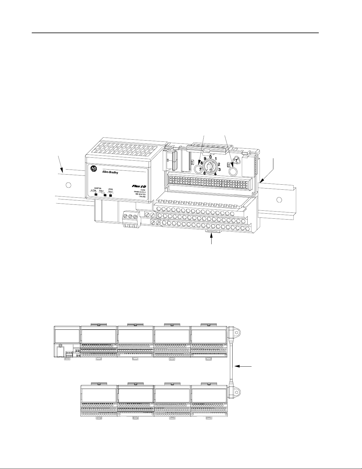
You can horizontally or vertically mount the FLEX I/O system on
a standard DIN rail. The adapter and terminal base easily snap on the
DIN rail by hand. Refer to the installation instructions shipped with
these components.
Screw holes are also provided to horizontally or vertically
panel-mount your system in an enclosure. To panel-mount your
FLEX I/O system, use the optional mounting kit (1794-NM1).
An example of a DIN rail-mounted system is shown below.
Screw holes are available
for panel-mounting.
Components are
slotted to accept a
DIN rail.
Optional Accessories
Locking tab connector holds
terminal base onto DIN rail.
20127
Extender Cables (1794-CE1 or -CE3)
Use the optional 1794-CE1 (0.3m) or -CE3 (0.9m) extender cable
(one per system) to arrange your system in two rows or split your
system into horizontal and vertical orientation.
1794-CE1 or -CE3
Extender Cable
Publication 1794-6.5.6 – April 1996
20129
Page 12
Overview of FLEX I/O and Your PROFIBUS Adapter Module 1–3
ATTENTION: This cable can only be used between
I/O modules. Do not use between the adapter and I/O
!
modules. Do not use more than one cable per system.
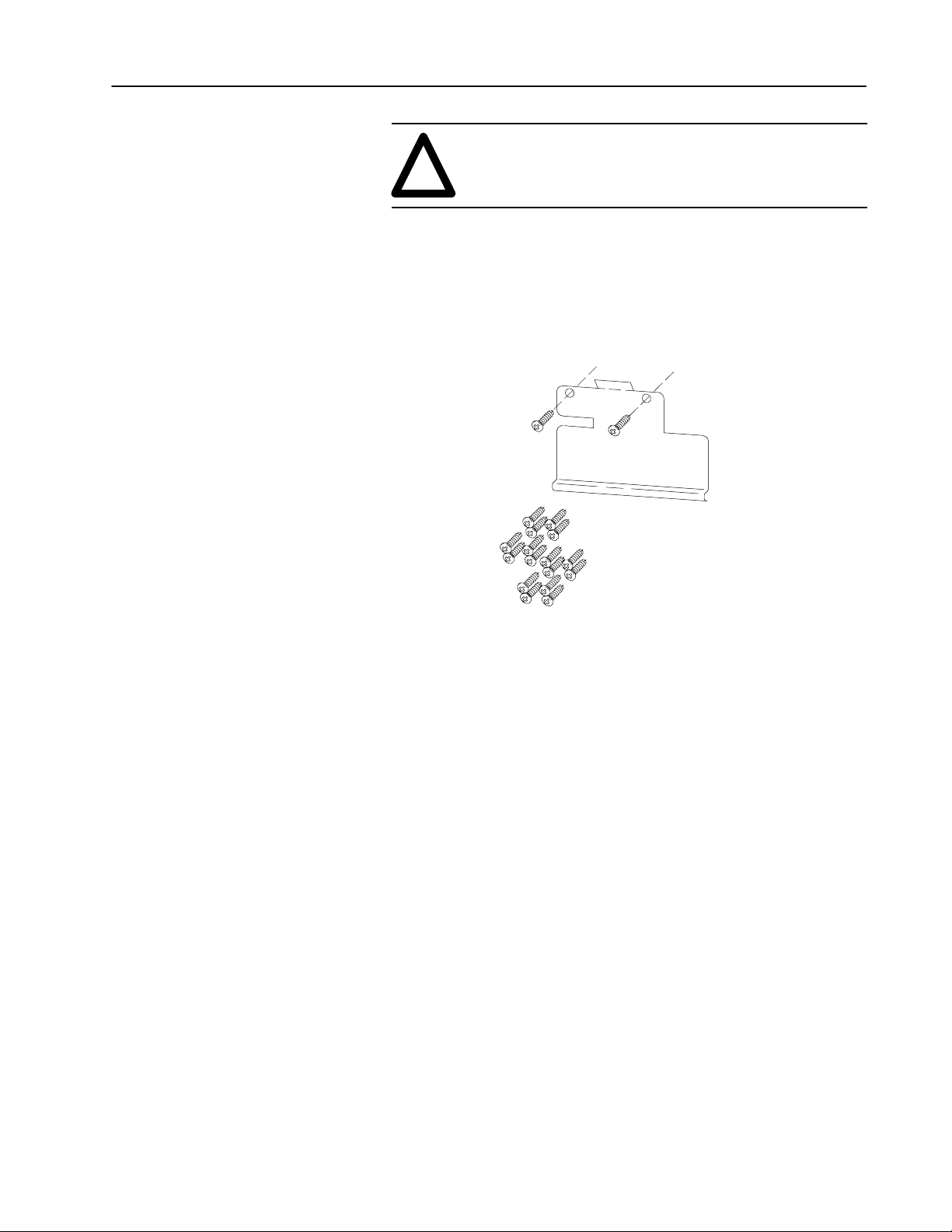
Mounting Kit (1794-NM1)
Use the optional 1794-NM1 mounting kit to mount your system on a
panel or wall without a DIN rail.
1794-NM1
Mounting Kit with
18 screws (2 screws for
the adapter and 2 screws
for each module)
20129
Publication 1794-6.5.6 – April 1996
Page 13
Overview of FLEX I/O and Your PROFIBUS Adapter Module 1–4
Mounting Dimensions and Spacing Requirements
.83
(21)
3.2
(80)
3.4
(87)
Allow 1.0 (25.4) air
gap on all 4 sides.
1794-ASB
3.4H x 2.7W x 2.7D
(87H x 68W x 69D)
Optional
Mounting
Kit
1.4
(35)
2.7
(68)
2.3
(59)
Inches
(Millimeters)
1.4
(35)
3.7
(94)
3.7
(94)
1794-TB2, -TB3
3.7H x 3.7W x 2.7D
(94H x 94W x 69D)
0.9
(23)
DIN
Rail
0.6
(17.0)
0.3
(8)
2.0
(50)
1.2
(30)
Approximately
11.5 (292.1)
from upper
connector
3.7
(94)
3.2
(80)
Publication 1794-6.5.6 – April 1996
Secure DIN Rail
every 200mm.
Page 14
Overview of FLEX I/O and Your PROFIBUS Adapter Module 1–5
Purpose of the 1794-APB FLEX I/O Adapter
= Drop Cable
= Bus Segment
= Termination Block
= T–junction
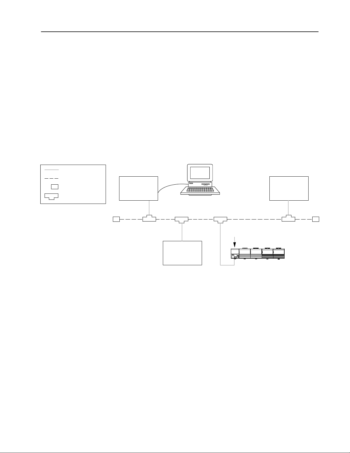
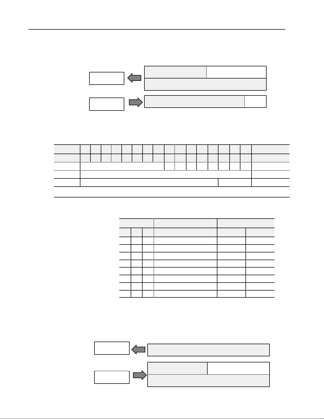
The 1794-APB is a FLEX I/O adapter that interacts with the FLEX
I/O backplane and any PROFIBUS DP master/scanner controller on
a PROFIBUS DP network.
The 1794-APB module is a slave device to the DP master/scanner,
and is a master controller of the FLEX I/O system where it is
installed.
The I/O data exchange occurs as follows: Output data is sent from
the DP master/scanner controller across the PROFIBUS DP network
to the 1794-APB adapter. The adapter then automatically transfers
the data across the FLEX I/O backplane to the output modules.
Inputs from the input modules are collected by the FLEX I/O adapter
via the backplane and sent across the PROFIBUS DP network to the
DP master/scanner controller.
PROFIBUS DP
Master/Scanner
Controller
RS-232
Personal Computer
with Configuration
Software
Other DP
Adapter/Slave
Other DP
Adapter/Slave
DP
1794-APB Adapter Slave
FLEX I/O System
Publication 1794-6.5.6 – April 1996
Page 15
Overview of FLEX I/O and Your PROFIBUS Adapter Module 1–6
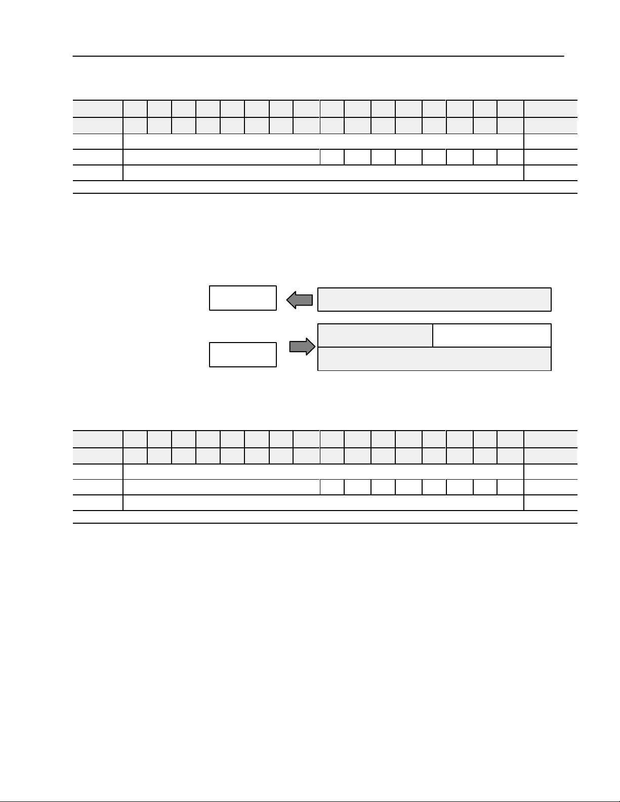
PROFIBUS Adapter Components
STATUS indicator
(green/red)
PROFIBUS indicator
(green/red)
The adapter module consists of the following components:
• two diagnostic indicators
• PROFIBUS DP network connector
• 24V dc power wiring connection terminals
• two node address switches
Flexbus
Connector
24V dc wiring
Connection
Terminals
PROFIBUS
DP
Network
Connector
More
Node Address
Switches
Information...
20627
Diagnostic
Indicators
Diagnostic indicators are located on the front panel of the adapter
module. They show both normal operation and error conditions in
your FLEX I/O system. The indicators are:
• Device status (STATUS)
• Communication link status (PROFIBUS)
Upon power-up, the adapter goes to an initialization state and
performs a self-test (memory check, data memory clear, CRC on
code). The indicators also go through a self-test sequence. If a failure
occurs, the adapter transitions to a faulted state and waits for reset
(cycle power). Otherwise, the adapter begins monitoring the network
(run state) for messages.
Chapter 5 describes the diagnostic indicators and how to use them
for troubleshooting.
Publication 1794-6.5.6 – April 1996
Page 16

Overview of FLEX I/O and Your PROFIBUS Adapter Module 1–7
Network Connector
Use the 9-pin D-shell connector to connect your adapter to the
PROFIBUS network.
Setting the Node Address Switches
Set the node address using the 2-position thumbwheel switch. Valid
settings range from 01 to 99. Use a pen to press either the + or –
buttons to change the number.
More
Information...
PROFIBUS
DP Network
Connector (9-pin
D-shell)
Node
Address
Switches
24V dc wiring
Connection
Terminals
Power Wiring
Connections are provided for connecting the required 24V dc power
to the front of the module. The power wiring can be daisy-chained to
the terminal base unit located next to the adapter to supply power to
the module installed in that base unit.
Refer to the Installation Instructions (pub. no. 1794-5.40) you
received with your adapter to learn how to install and wire the
adapter.
Publication 1794-6.5.6 – April 1996
Page 17

Overview of FLEX I/O and Your PROFIBUS Adapter Module 1–8
Publication 1794-6.5.6 – April 1996
Page 18
Chapter 2
How Communication Takes
Place and I/O Image Table
Mapping
What
this Chapter Contains
Communication Over the I/O Backplane
Network
PROFIBUS
Adapter
Read
Write
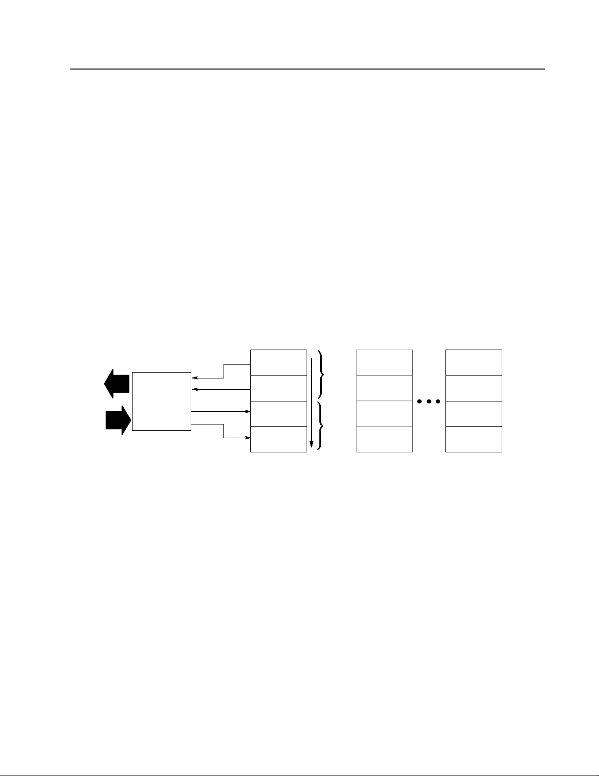
In this chapter, you will learn about:
• communication over the FLEX I/O backplane (between the
PROFIBUS adapter and the I/O modules)
• how data is mapped into the I/O image table
One 1794-APB PROFIBUS adapter can interface with up to eight
terminal base units with installed FLEX I/O modules, forming a
FLEX I/O system of up to eight slots. The adapter communicates to
other network system components over the PROFIBUS network.
The adapter communicates with its I/O modules over the backplane.
I/O Module
Inputs
Status
Outputs
Configuration
Slot
1
0
Read
Words
Write
Words
15
I/O Module
Inputs
Status
Outputs
Configuration
Slot 2
I/O Module
Inputs
Status
Outputs
Configuration
Slot 8
The I/O map for a module is divided into read words and write
words. Read words consist of input and status words, and write
words consist of output and configuration words. The number of
read words or write words can be 0 or more. The length of each I/O
module’s read words and write words vary in size depending on
module complexity. Each I/O module will support at least 1 input
word or 1 output word. Status and configuration are optional,
depending on the module.
Publication 1794-6.5.6 – April 1996
Page 19
How Communication Takes Place and I/O Image Table Mapping 2–2
For example, a 16 point discrete input module will have up to 2 read
words and 1 write word.
Polled I/O Structure
16-point
Discrete Input Module
I/O Image
Input Size
1 or 2 W
ords
Output Size
0 or 1 W
ord
Module Image
Not used
Inputs
Not used
Delay
Time
Delay
Time
Check the I/O map for each module for the exact mapping.
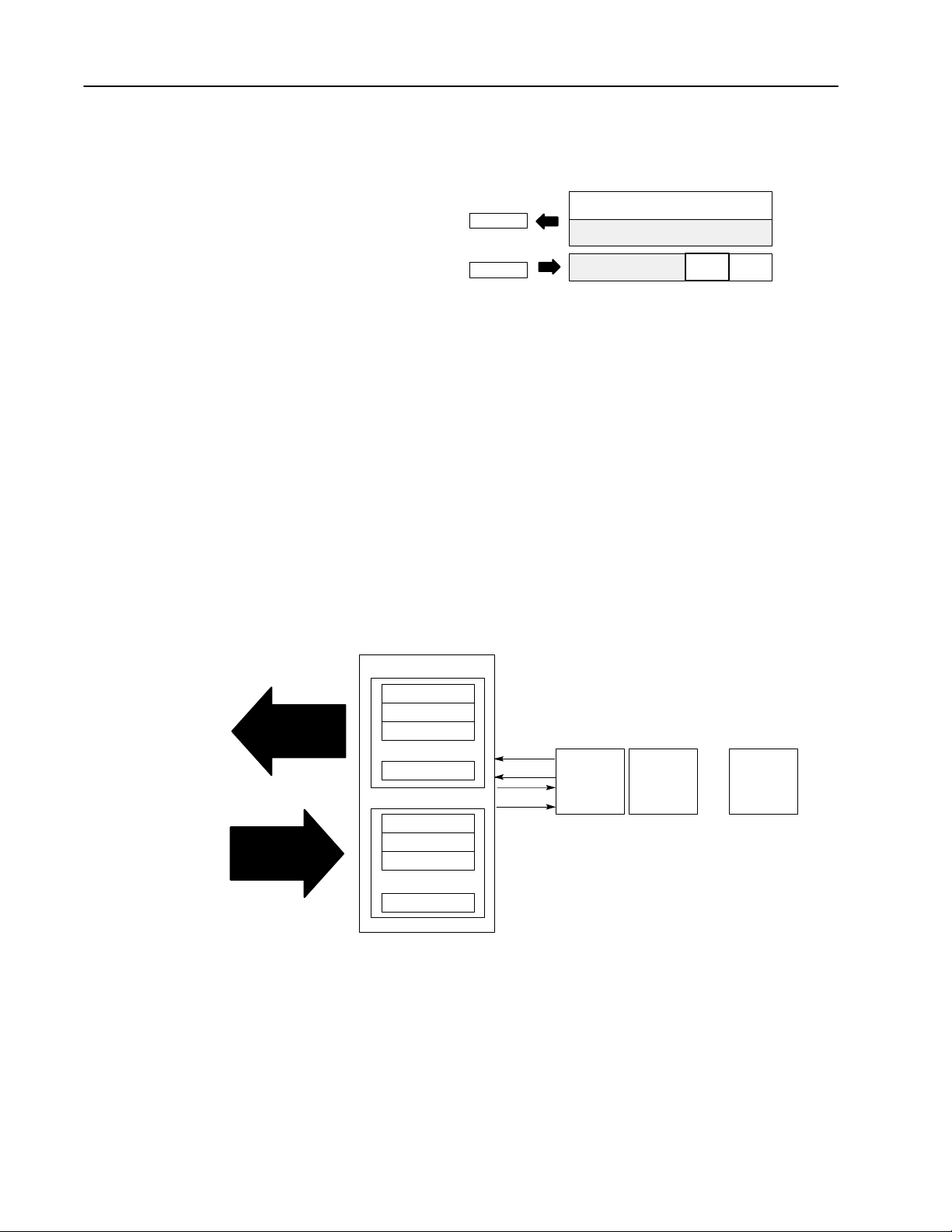
The first word of output data sent by the adapter is the Adapter
Status Word. Output data is received by the adapter in the order of
the installed I/O modules. The Output data for Slot 1 is received
first, followed by the Output data for Slot 2, and so on up to slot 8.
All bits in the output status word are reserved
The first word of input data sent by the adapter is the Adapter Status
Word. This is followed by the input data from each slot, in the order
of the installed I/O modules. The Input data from Slot 1 is first after
the status word, followed by Input data from Slot 2, and so on up to
slot 8.
Network READ
Network WRITE
PROFIBUS Adapter
Read Data
Adapter Status
Slot 1 Input Data
Slot 2 Input Data
...
Slot 8 Input Data
Write Data
Adapter Status
Slot 1 Output Data
Slot 2 Output Data
...
Slot 8 Output Data
...
...
Read
Write
I/O Module
Slot 1
I/O Module
Slot 2
...
I/O Module
Slot 8
Publication 1794-6.5.6 – April 1996
Page 20
How Communication Takes Place and I/O Image Table Mapping 2–3
I/O Module Faul
Adapter Input Status Word
The input status word consists of:
• I/O module fault bits – 1 status bit for each slot
• node address changed – 1 bit
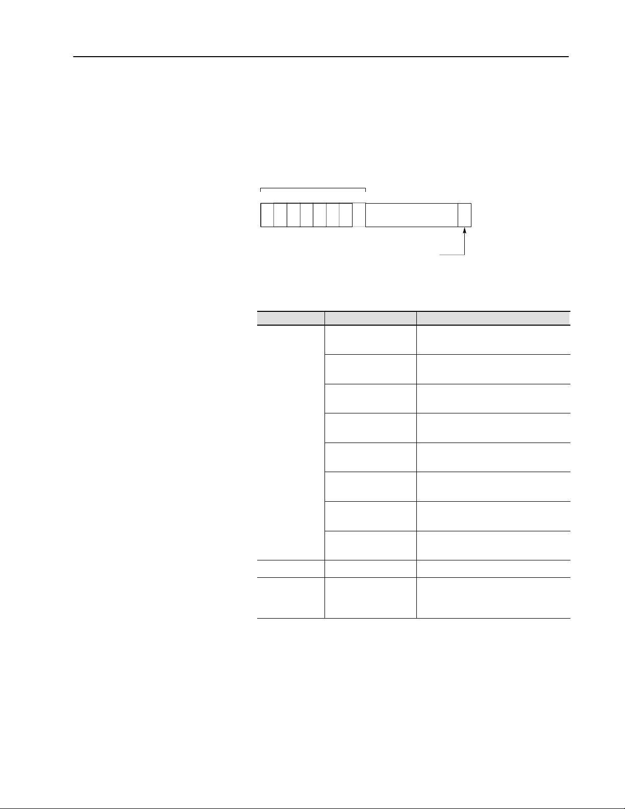
I/O Module Fault Bits
15Bit: 01234567
814 13 12 11 10 19
Slot 8
Slot 7
Slot 6
Slot 5
Slot 1
Slot 2
Slot 3
Slot 4
Node Address Changed Bit
Reserved
The adapter input status word bit descriptions are shown in the
following table.
Bit Description Bit Explanation
8
9
10
11
t
12
13
14
This bit is set (1) when an error is detected
in slot position 1.
This bit is set (1) when an error is detected
in slot position 2.
This bit is set (1) when an error is detected
in slot position 3.
This bit is set (1) when an error is detected
in slot position 4.
This bit is set (1) when an error is detected
in slot position 5.
This bit is set (1) when an error is detected
in slot position 6.
This bit is set (1) when an error is detected
in slot position 7.
15
Reserved 1–7 Reserved
Node Address
Changed
0
This bit is set (1) when an error is detected
in slot position 8.
This bit is set (1) when the node address
switch setting has been changed since
power up.
Possible causes for an I/O module fault are:
• transmission errors on the FLEX I/O backplane
• a failed module
• a module removed from its terminal base
• incorrect module inserted in a slot position
• the slot is empty
Publication 1794-6.5.6 – April 1996
Page 21
How Communication Takes Place and I/O Image Table Mapping 2–4
The node address changed bit is set when the node address switch
setting has been changed since power up. The new node address does
not take affect until the adapter has been powered down and then
powered back up. Until this power cycling occurs, the node address
switches will not match the actual node address.
Mapping
Data into
the Image Table
All FLEX I/O modules are supported by the PROFIBUS adapter.
Presently, these consist of:
Module Description Catalog Number
16 Sink Input Module 1794-IB16 page 2–4
16 Source Output Module 1794-OB16 page 2–6
8 Sensor Input Module 1794-IB8S page 2–7
8 Input Module 1794-IA8 page 2–8
8 Output Module 1794-OA8 page 2–8
8 Relay Output Module 1794-OW8 page 2–9
8 Input Analog Module 1794-IE8 page 2–10
4 Output Analog Module 1794-OE4 page 2–12
4 in/2 out Analog Combo Module 1794-IE4XOE2 page 2–15
8 Input RTD Analog Module 1794-IR8 page 2–17
8 Input Thermocouple Module 1794-IT8 page 2–21
SCANport Module 1203-FM1 page 2–25
For image table
mapping, refer to:
Read
Write
I/O Image
Input Size
1 or 2 Words
Output Size
0 or 1 Word
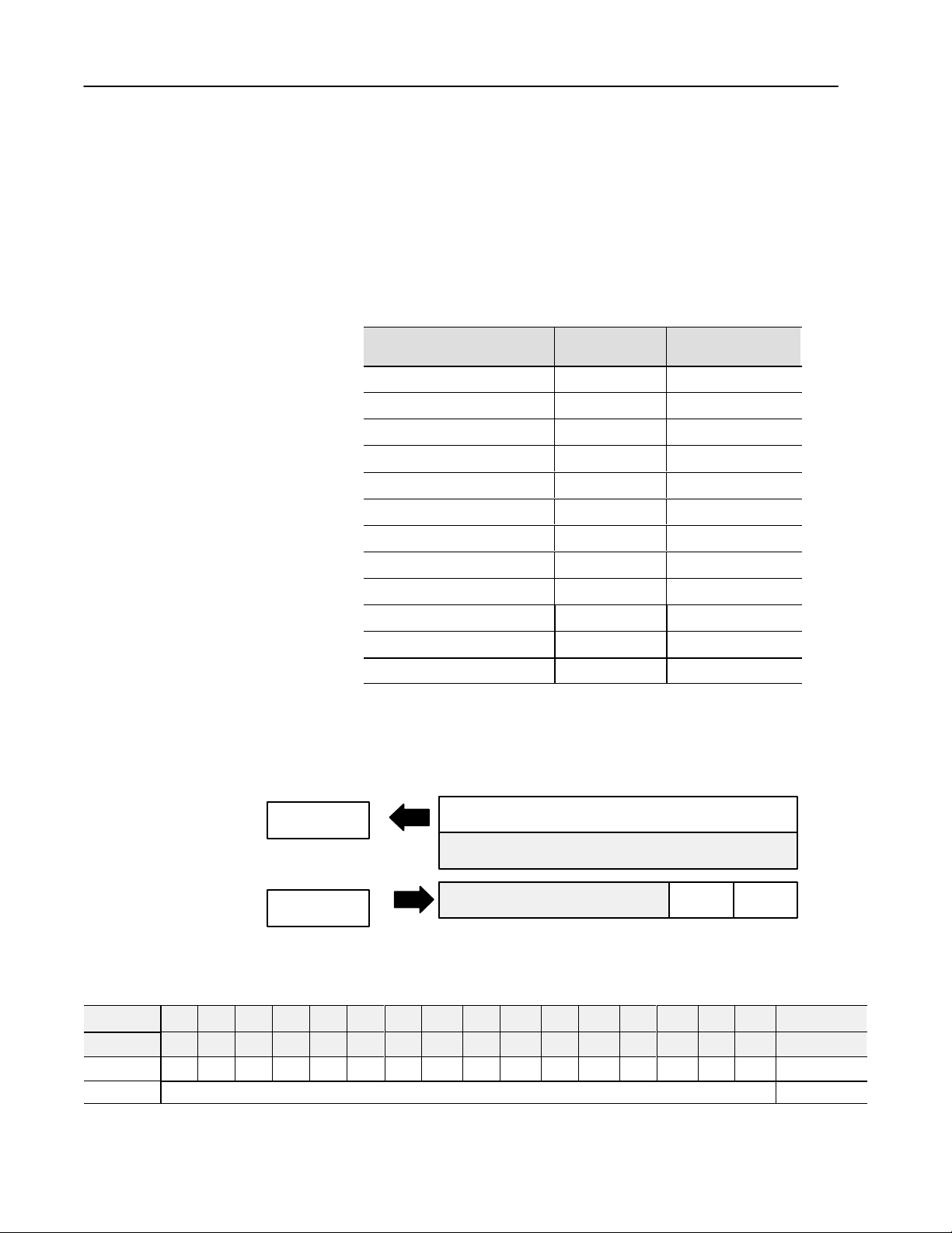
1794-IB16 – 16-point Discrete Input Module Image T
Module
Image
Inputs
Not used
Not used
Delay
Time
able Mapping
Delay
Time
1794-IB16 Memory Map
Decimal Bit 15 14 13 12 11 10 09 08 07 06 05 04 03 02 01 00 Size
Octal Bit
Publication 1794-6.5.6 – April 1996
17 16 15 14 13 12 11 10 07 06 05 04 03 02 01 00 Read Words
D15 D14 D13 D12 D11 D10 D9 D8 D7 D6 D5 D4 D3 D2 D1 D0 Read Word 1
Not used Read Word 2
Page 22

How Communication Takes Place and I/O Image Table Mapping 2–5
Octal Bit
Not used DT 12–15 DT 00–11 Write Word 1
Where D = Input Data (D0 corresponds to input 0, D1 corresponds to input 1, etc.
DT = Input Delay T
ime (DT 00–1
1 corresponds to inputs 0 thru 1
1; DT 12–15 corresponds to inputs 12 thru 15)
Read Words00010203040506071011121314151617
Publication 1794-6.5.6 – April 1996
Page 23
How Communication Takes Place and I/O Image Table Mapping 2–6
y
Delay Time
I/O Image
Input Size
1794-IB16
Input Delay T
imes
Bits Description
02 01 00 Delay Time for Inputs 00–11
Selected
Dela
Time
05 04 03 Delay Time for Inputs 12–15
0 0 0 Delay Time 0 (default) 512µs
0 0 1 Delay Time 1 1ms
0 1 0 Delay Time 2 2ms
0 1 1 Delay Time 3 4ms
1 0 0 Delay Time 4 8ms
1 0 1 Delay Time 5 16ms
1 1 0 Delay Time 6 32ms
1 1 1 Delay Time 7 64ms
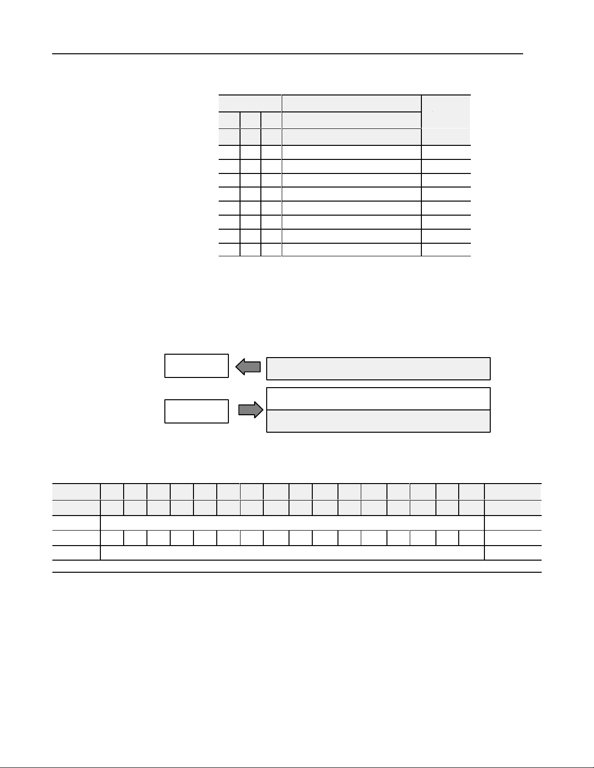
1794-OB16 – 16-point Discrete Output Module Image Table
Mapping
Module
Image
Read
Write
0 or 1 Word
Output Size
1 or 2 Words
Not used
Outputs
Not used
1794-OB16 Memory Map
Decimal Bit 15 14 13 12 11 10 09 08 07 06 05 04 03 02 01 00 Size
Octal. Bit 17 16 15 14 13 12 11 10 07 06 05 04 03 02 01 00 Read Words
Not used Read Word 1
O15 O14 O13 O12 O11 O10 O9 O8 O7 O6 O5 O4 O3 O2 O1 O0 Write Word 1
Not used Write Word 2
Where O
= Output value (O0 corresponds to output 0, O1 corresponds to output 1, etc.)
Publication 1794-6.5.6 – April 1996
Page 24
How Communication Takes Place and I/O Image Table Mapping 2–7
y
Delay Time
1794-IB8S – 8-point Discrete Sensor Input Module Image Table
Mapping
I/O Image
Module
Image
Input Size
Read
1 or 2 Words
Status
Inputs
Not used
Output Size
Write
0 or 1 Word
Not used
Delay
Time
Delay
Time
1794-IB8S Memory Map
Decimal Bit 15 14 13 12 11 10 09 08 07 06 05 04 03 02 01 00 Size
Octal Bit 17 16 15 14 13 12 11 10 07 06 05 04 03 02 01 00 Read Words
S7 S6 S5 S4 S3 S2 S1 S0 D7 D6 D5 D4 D3 D2 D1 D0 Read Word 1
Not used Read Word 2
Not used DT 12–15 DT 00–11 Write Word 1
Where S = Status of input (where S1 corresponds to the diagnostic bit for input 1, S2 corresponds to the diagnostic bit for input 2, etc.)
D = Input Data (where D0 corresponds to input 0, D1 corresponds to input 1, etc.
DT = Input Delay T
Make certain that the delay time for 00–11 is the same as the delay time for 12–15.
Smart Sensor
Bits
S = Diagnostic data – 1 = Fault present (Smart)
08–15
Standard Sensor
Bits
S = Diagnostic data – 1 = Diagnostics not disabled
08–15
ime (where DT 00–1
0 = Normal (no errors)
0 = Normal (Disabled)
1 corresponds to inputs 0 thru 1
1; DT 12–15 corresponds to inputs 12 thru 15.
Bits
D = Input data 1 = Sensor on
00–07
Bits
D = Input data 1 = Sensor on
00–07
0 = Sensor off
0 = Sensor off
1794-IB8S
Input Delay T
imes
Bits Description
02 01 00 Delay Time for Inputs 00–11
Dela
05 04 03 Delay Time for Inputs 12–15
0 0 0 Delay Time 0 (default) 512µs
0 0 1 Delay Time 1 1ms
0 1 0 Delay Time 2 2ms
0 1 1 Delay Time 3 4ms
1 0 0 Delay Time 4 8ms
1 0 1 Delay Time 5 16ms
1 1 0 Delay Time 6 32ms
1 1 1 Delay Time 7 64ms
Publication 1794-6.5.6 – April 1996
Selected
Time
Page 25
How Communication Takes Place and I/O Image Table Mapping 2–8
Read
Write
I/O Image
Input Size
1 or 2 Words
Output Size
0 or 1 Word
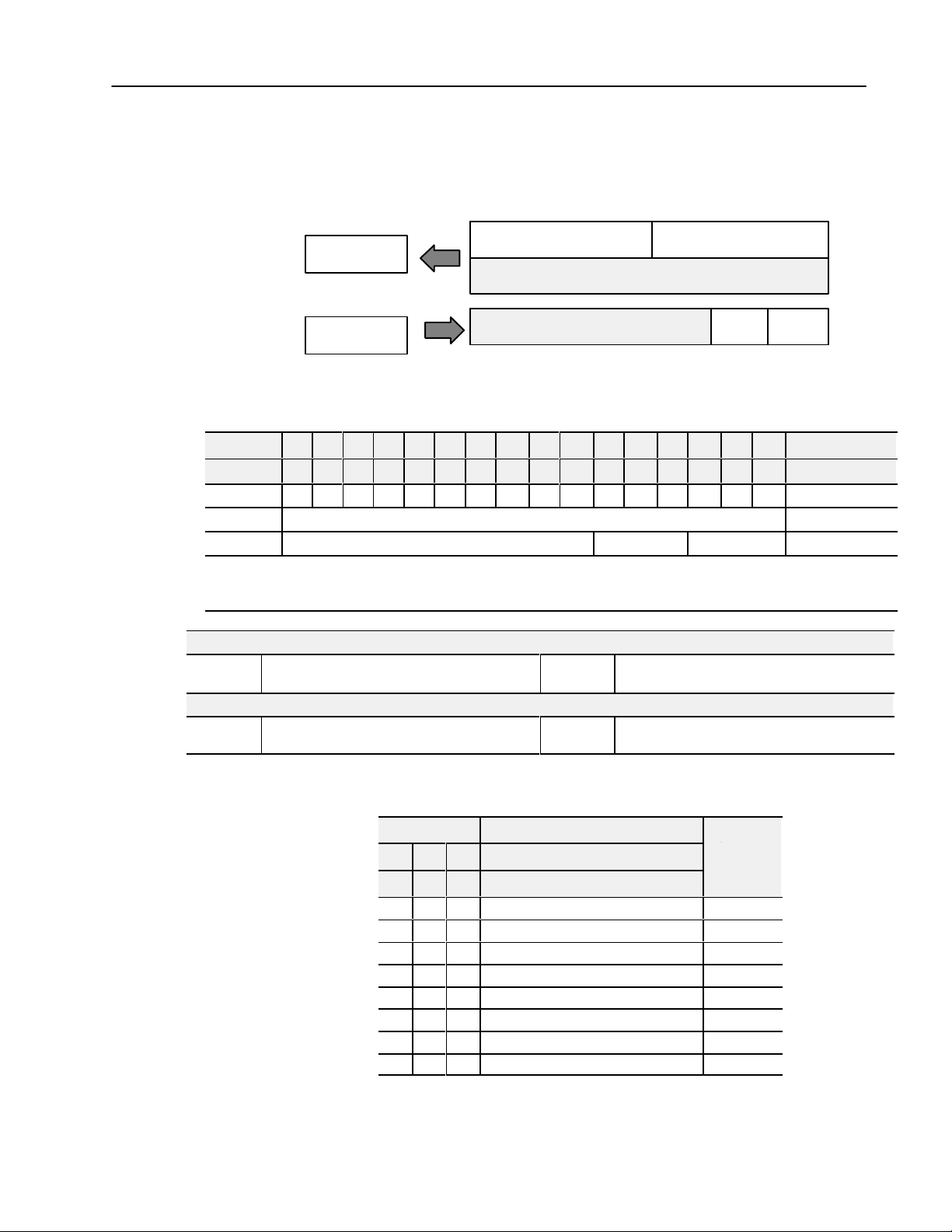
1794-IA8 – 8-point Discrete Input Module Image T
Module
Image
Not used
Not used
Not used
able Mapping
Inputs
Delay
Time
1794-IA8 Memory Map
Decimal Bit 15 14 13 12 11 10 09 08 07 06 05 04 03 02 01 00 Size
Octal Bit 17 16 15 14 13 12 11 10 07 06 05 04 03 02 01 00 Read Words
Not used D7 D6 D5 D4 D3 D2 D1 D0 Read Word 1
Not used Read Word 2
Not used DT 00–07 Write Word 1
Where D = Input Data (where D0 corresponds to input 0, D1 corresponds to input 1, etc.
DT = Input Delay T
ime (where DT 00–07 corresponds to inputs 0 thru 7)
Read
I/O Image
Input Size
0 or 1 Word
1794-IA8
Input Delay T
Bits Description Maximum Delay Time
02 01 00 Delay Time for Inputs 00–07 Off to On On to Off
0 0 0 Delay Time 0 (default) 8.6ms 26.6ms
0 0 1 Delay Time 1 9ms 27ms
0 1 0 Delay Time 2 10ms 28ms
0 1 1 Delay Time 3 12ms 30ms
1 0 0 Delay Time 4 17ms 35ms
1 0 1 Delay Time 5 26ms 44ms
1 1 0 Delay Time 6 43ms 61ms
1 1 1 Delay Time 7 78ms 96ms
1794-OA8 – 8-point Discrete Output Module Image T
imes
Module
Not used
able Mapping
Image
Publication 1794-6.5.6 – April 1996
Write
Output Size
1 or 2 Words
Not used
Outputs
Not used
Page 26
How Communication Takes Place and I/O Image Table Mapping 2–9
1794-OA8
Decimal Bit 15 14 13 12 11 10 09 08 07 06 05 04 03 02 01 00 Size
Oct. Bit 17 16 15 14 13 12 11 10 07 06 05 04 03 02 01 00 Read Words
Not used O7 O6 O5 O4 O3 O2 O1 O0 Write Word 1
Where O
= Output value (where O0 corresponds to output 0, O1 corresponds to output 1, etc.)
Memory Map
Not used Read Word 1
Not used Write Word 2
1794-OW8 – 8-point Discrete Relay Output Module Image Table
Mapping
I/O Image
Module
Image
Not used
Outputs
Not used
Read
Write
Input Size
0 or 1 Word
Output Size
1 or 2 Words
Not used
1794-OW8 Memory Map
Decimal Bit 15 14 13 12 11 10 09 08 07 06 05 04 03 02 01 00 Size
Oct. Bit 17 16 15 14 13 12 11 10 07 06 05 04 03 02 01 00 Read Words
Not used Read Word 1
Not used O7 O6 O5 O4 O3 O2 O1 O0 Write Word 1
Not used Write Word 2
Where O = Output value: where O0 corresponds to output 0, O1 corresponds to output 1, etc., and when bit = 0, the output is off; when bit = 1, the output is on.
Publication 1794-6.5.6 – April 1996
Page 27
How Communication Takes Place and I/O Image Table Mapping 2–10
1794-IE8
I/O Image
Input Size
1 to 9 Words
Output Size
0 or 1 Word
– 8 Input Analog Module
Input Data Channel 0
Input Data Channel 1
Input Data Channel 2
Input Data Channel 3
Input Data Channel 4
Input Data Channel 5
Input Data Channel 6
Input Data Channel 7
PU
Configure select
Module
Not used
Not used
Not used
Not used
Not used
Image
Underrange
1794-IE8 Memory Map
Decimal
Bit
Oct. Bit 17 16 15 14 13 12 11 10 07 06 05 04 03 02 01 00 Read Words
Where: PU
15 14 13 12 11 10 09 08 07 06 05 04 03 02 01 00 Size
S Analog Value Channel 0 Read Word 1
S Analog Value Channel 1 Read Word 2
S Analog Value Channel 2 Read Word 3
S Analog Value Channel 3 Read Word 4
S Analog Value Channel 4 Read Word 5
S Analog Value Channel 5 Read Word 6
S Analog Value Channel 6 Read Word 7
S Analog Value Channel 7 Read Word 8
PU Not used – set to zero U7 U6 U5 U4 U3 U2 U1 U0 Read Word 9
C7 C6 C5 C4 C3 C2 C1 C0 F7 F6 F5 F4 F3 F2 F1 F0 Write Word 1
Not used – set to 0 Write Word 2 thru 6
= Power up bit – included in series B modules only
U = Underrange bits for 4-20mA inputs
C = Configure select bit
F = Full range bit
S = sign bit (in 2’
s complement)
.
Publication 1794-6.5.6 – April 1996
Page 28

How Communication Takes Place and I/O Image Table Mapping 2–11
Read Word 1
Read Word 2
Read Word 3
Read Word 4
Read Word 5
Read Word 6
Read Word 7
Read Word 8
1794-IE8
Range Selection Bits
Channel No. Channel 0 Channel 1 Channel 2 Channel 3 Channel 4 Channel 5 Channel 6 Channel 7
F0 C0 F1 C1 F2 C2 F3 C3 F4 C4 F5 C5 F6 C6 F7 C7
Decimal Bit 00 08 01 09 02 10 03 11 04 12 05 13 06 14 07 15
0–10V dc/0–20mA 1 0 1 0 1 0 1 0 1 0 1 0 1 0 1 0
4–20mA 0 1 0 1 0 1 0 1 0 1 0 1 0 1 0 1
-10 to +10V dc 1 1 1 1 1 1 1 1 1 1 1 1 1 1 1 1
Do Not Use
C
= Configure select bit
F = Full range bit
1
Do not use this configuration. Individual channels revert to 4–20mA if bit selection is all zeroes.
1
0 0 0 0 0 0 0 0 0 0 0 0 0 0 0 0
1794-IE8 Word/Bit Descriptions
Word Decimal Bit Definition
Read Word 1
Bits 00–14
Bits 15 Channel 0 analog data sign bit.
Bits 00–14
Read Word 2
Bits 15 Channel 1 analog data sign bit.
Bits 00–14
Read Word 3
Bits 15 Channel 2 analog data sign bit.
Bits 00–14
Read Word 4
Bits 15 Channel 3 analog data sign bit.
Bits 00–14
Read Word 5
Bits 15 Channel 4 analog data sign bit.
Bits 00–14
Read Word 6
Bits 15 Channel 5 analog data sign bit.
Bits 00–14
Read Word 7
Bits 15 Channel 6 analog data sign bit.
Bits 00–14
Read Word 8
Bits 15 Channel 7 analog data sign bit.
Channel 0 analog data – 12-bit left justified two’s complement
number; unused lower bits are zero; 4-20mA uses all 16 bits.
Channel 1 analog data – 12-bit left justified two’s complement
number; unused lower bits are zero; 4-20mA uses all 16 bits.
Channel 2 analog data – 12-bit left justified two’s complement
number; unused lower bits are zero; 4-20mA uses all 16 bits.
Channel 3 analog data – 12-bit left justified two’s complement
number; unused lower bits are zero; 4-20mA uses all 16 bits.
Channel 4 analog data – 12-bit left justified two’s complement
number; unused lower bits are zero; 4-20mA uses all 16 bits.
Channel 5 analog data – 12-bit left justified two’s complement
number; unused lower bits are zero; 4-20mA uses all 16 bits.
Channel 6 analog data – 12-bit left justified two’s complement
number; unused lower bits are zero; 4-20mA uses all 16 bits.
Channel 7 analog data – 12-bit left justified two’s complement
number; unused lower bits are zero; 4-20mA uses all 16 bits.
Publication 1794-6.5.6 – April 1996
Page 29

How Communication Takes Place and I/O Image Table Mapping 2–12
Wri
1
DefinitionDecimal BitWord
Underrange bits (U) for individual channels (4-20mA current
input only)– Bit 00 corresponds to input channel 0, bit 01
Bits 00–07
Read Word 9
te Word
Write Word 2 Bits 00–15 Not used – set to 0.
Write Word 3 Bits 00–15 Not used – set to 0.
Write Word 4 Bits 00–15 Not used – set to 0.
Write Word 5 Bits 00–15 Not used – set to 0.
Write Word 6 Bits 00–15 Not used – set to 0.
Bits 08-14
Bit 15
Bits 00–07
Bits 08–15
corresponds to input channel 1, and so on. When set (1),
indicates either a broken or open input wire, or input current
below 4-20mA.
Not used – set to 0.
Power Up bit – included in series B modules only. This bit
is 0 in series A modules. This bit is set to 1 when all bits in
the configuration register are 0 (unconfigured state). The
configuration register can be cleared by either of the reset
inputs, or by the user writing all zeroes to it.
Full range bits (F) for individual channels – Bit 00 corresponds
to input channel 0, bit 01 corresponds to input channel 1, and
so on. Refer to range selection above.
Configure select bits (C) for individual channels – Bit 08
corresponds to input channel 0, bit 09 corresponds to input
channel 1, and so on. Refer to range selection above.
Read
Write
1794-OE4
I/O Image
Input Size
0 or 1 Word
Output Size
1 or 6 Words
– 4 Output Analog Module Image T
Module
Image
PU
Not used Not used
Config. Select
Not used
Analog Data Channel 0
Analog Data Channel 1
Analog Data Channel 2
Analog Data Channel 3
Not used
Not used
Not used
Not used
Not used
Not used
Not used
Not used
Not used
able Mapping
Diagnostics
OE
Full Range
Publication 1794-6.5.6 – April 1996
Page 30

How Communication Takes Place and I/O Image Table Mapping 2–13
d
Read
Write Word 1
Decimal
1794-OE4
15 14 13 12 11 10 09 08 07 06 05 04 03 02 01 00 Size
Memory Map
Bit
Oct. Bit 17 16 15 14 13 12 11 10 07 06 05 04 03 02 01 00 Read Words
PU Not used – set to 0 W3 W2 W1 W0 Read Word 1
S Analog Data – Channel 0 Write Word 1
S Analog Data – Channel 1 Write Word 2
S Analog Data – Channel 2 Write Word 3
S Analog Data – Channel 3 Write Word 4
Not used – set to 0 OE3 OE2 OE1 OE0 Write Word 5
Not used – set to 0 C3 C2 C1 C0 Not used – set to 0 F3 F2 F1 F0 Write Word 6
Not used – set to 0
Where: PU
= Power up bit – included in series B modules only
W = Diagnostic bits for current output wire broken or load resistance high. (Not used on voltage outputs.)
S = Sign bit (in 2’
OE = Output enable bits (bit 00 corresponds to output 0, bit 01 corresponds to output 1 and so on.
set to 1.
C = Configure select bit
F = Full range bit
s complement)
.
1794-OE4
Range Selection Bits (W
ATTENTION: These bits must be
rite W
ord 6)
Write W
thru 14
ords 7
Channel No. Channel 0 Channel 1 Channel 2 Channel 3
F0 C0 F1 C1 F2 C2 F3 C3
Decimal Bit 00 08 01 09 02 10 03 11
4–20mA 0 1 0 1 0 1 0 1
0–10V dc/0–20mA 1 0 1 0 1 0 1 0
-10 to +10V dc 1 1 1 1 1 1 1 1
1
Off
C
= Configure select bit
F = Full range bit
1
When configured to of
f, individual channels will return 0V
0 0 0 0 0 0 0 0
.
1794-OE4 Word/Bit Descriptions
Word Decimal Bit Definition
Current outputs only – When set (1), the wire on the output is
broken or the load resistance is too high. Bit 00 corresponds to
channel 0, bit 01 corresponds to channel 2, and so on.
Power Up bit – included in series B modules only. This bit
is 0 in series A modules. This bit is set to 1 when all bits in
the configuration register are 0 (unconfigured state). The
configuration register can be cleared by either of the reset
inputs, or by the user writing all zeroes to it.
Rea
Word 1
Bits 00-03
Bits 04-14 Not used – set to 0.
Bit 15
Write Word 1
Bits 00–14
Channel 0 analog data – 12-bit left justified two’s complement
number; unused lower bits are zero; 4-20mA uses all 16 bits.
Bits 15 Channel 0 analog data sign bit.
Publication 1794-6.5.6 – April 1996
Page 31

How Communication Takes Place and I/O Image Table Mapping 2–14
Write Word 2
Write Word 3
Write Word 4
Wri
6
DefinitionDecimal BitWord
Write Word 2
Bits 00–14
Channel 1 analog data – 12-bit left justified two’s complement
number; unused lower bits are zero; 4-20mA uses all 16 bits.
Bits 15 Channel 1 analog data sign bit.
Write Word 3
Bits 00–14
Channel 2 analog data – 12-bit left justified two’s complement
number; unused lower bits are zero; 4-20mA uses all 16 bits.
Bits 15 Channel 2 analog data sign bit.
Write Word 4
Bits 00–14
Channel 3 analog data – 12-bit left justified two’s complement
number; unused lower bits are zero; 4-20mA uses all 16 bits.
Bits 15 Channel 3 analog data sign bit.
Output Enable bits. Bit 00 corresponds to input 0, bit 01
Write Word 5
Bits 00–03
corresponds to input 1, bit 02 corresponds to input 2, and bit 03
corresponds to input 3. These bits must be set to 1.
Bits 04-15 Not used – set to 0.
Full range bits (F) for individual channels – Bit 00 corresponds
Bits 00–03
to output channel 0, bit 01 corresponds to output channel 1,
and so on. Refer to range selection above.
Bits 04-07 Not used – set to 0.
te Word
Bits 08–11
Configure select bits (C) for individual channels – Bit 08
corresponds to output channel 0, bit 09 corresponds to output
channel 1, and so on. Refer to range selection above.
Bits 12-15 Not used – set to 0.
Write Word 7 Bits 00–15 Not used – set to 0.
Write Word 8 Bits 00–15 Not used – set to 0.
Write Word 9 Bits 00–15 Not used – set to 0.
Write Word 10 Bits 00–15 Not used – set to 0.
Write Word 11 Bits 00–15 Not used – set to 0.
Write Word 12 Bits 00–15 Not used – set to 0.
Write Word 13 Bits 00–15 Not used – set to 0.
Write Word 14 Bits 00–15 Not used – set to 0.
Publication 1794-6.5.6 – April 1996
Page 32

How Communication Takes Place and I/O Image Table Mapping 2–15
Read
Write
1794-IE4XOE2 – Analog Combo Module Image T
Module
I/O Image
Input Size
0 to 5 Words
Output Size
0 to 4 Words
PU
Not used Full Range and Configure Select
Input Data Channel 0
Input Data Channel 1
Input Data Channel 2
Input Data Channel 3
Output Data Channel 0
Output Data Channel 1
Not used
Not used
Not used
Not used
Not used
Not used
Image
Not used
able Mapping
Underrange & Diag.
OE
1794-IE4XOE2 Memory Map
Decimal
Bit
Oct. Bit 17 16 15 14 13 12 11 10 07 06 05 04 03 02 01 00 Read Words
Where: PU
15 14 13 12 11 10 09 08 07 06 05 04 03 02 01 00 Size
S Analog Value Input Channel 0 Read Word 1
S Analog Value Input Channel 1 Read Word 2
S Analog Value Input Channel 2 Read Word 3
S Analog Value Input Channel 3 Read Word 4
PU Not used – set to 0 W1 W0 U3 U2 U1 U0 Read Word 5
S Analog Data – Output Channel 0 Write Word 1
S Analog Data – Output Channel 1 Write Word 2
Not used – set to 0 OE1 OE0 Write Word 3
Not used C5 C4 C3 C2 C1 C0 0 0 F5 F4 F3 F2 F1 F0 Write Word 4
Not used – set to 0 Write Word 5 thru 10
= Power up bit – included in series B modules only
W = Diagnostic bits for current output wire broken or load resistance high. (Not used on voltage outputs.)
U = Underrange bits for 4-20mA inputs
OE = Output enable bits (bit 00 corresponds to output 0, bit 01 corresponds to output 1).
S = Sign bit (in 2’
C = Configure select bit
F = Full range bit
s complement)
.
ATTENTION: These bits must be set to 1.
Publication 1794-6.5.6 – April 1996
Page 33

How Communication Takes Place and I/O Image Table Mapping 2–16
Read Word 1
Read Word 2
Read Word 3
Read Word 4
Read Word 5
Write Word 1
Write Word 2
1794-IE4XOE2
Channel No. Input
Channel 0
Range Selection Bits
Input
Channel 1
Input
Channel 2
Input
Channel 3
Output
Channel 0
Output
Channel 1
F0 C0 F1 C1 F2 C2 F3 C3 F4 C4 F5 C5
Decimal Bit 00 08 01 09 02 10 03 11 04 12 05 13
4–20mA 0 1 0 1 0 1 0 1 0 1 0 1
0–10V dc/0–20mA 1 0 1 0 1 0 1 0 1 0 1 0
-10 to +10V dc 1 1 1 1 1 1 1 1 1 1 1 1
1
Off
C
= Configure select bit
F = Full range bit
1
When configured to of
0 0 0 0 0 0 0 0 0 0 0 0
f, individual channels will return either 0V or 0mA.
1794-IE4XOE2 Word/Bit Descriptions
Word Decimal Bit Definition
Read Word 1
Bits 00–14
Bits 15 Channel 0 analog data sign bit.
Bits 00–14
Read Word 2
Bits 15 Channel 1 analog data sign bit.
Bits 00–14
Read Word 3
Bits 15 Channel 2 analog data sign bit.
Bits 00–14
Read Word 4
Bits 15 Channel 3 analog data sign bit.
Bits 00–03
Bits 04-05
Read Word 5
Bits 06–14 Not used – set to 0.
Bit 15
Bits 00–14
Write Word 1
Bits 15 Channel 0 analog data sign bit.
Bits 00–14
Write Word 2
Bits 15 Channel 1 analog data sign bit.
Channel 0 analog data – 12-bit left justified two’s complement
number; unused lower bits are zero; 4-20mA uses all 16 bits.
Channel 1 analog data – 12-bit left justified two’s complement
number; unused lower bits are zero; 4-20mA uses all 16 bits.
Channel 2 analog data – 12-bit left justified two’s complement
number; unused lower bits are zero; 4-20mA uses all 16 bits.
Channel 3 analog data – 12-bit left justified two’s complement
number; unused lower bits are zero; 4-20mA uses all 16 bits.
Underrange bits (U) for individual channels
(4-20mA current
inputs only) – Bit 00 corresponds to input channel 0, bit 01
corresponds to input channel 1, and so on.
Wire Off bits (W) – Current outputs only – When set (1), the
wire on the current output is broken or the load resistance is
too high. Bit 00 corresponds to channel 0, bit 01 corresponds to
channel 2, and so on.
Power Up bit – included in series B modules only. This bit
is 0 in series A modules. This bit is set to 1 when all bits in
the configuration register are 0 (unconfigured state). The
configuration register can be cleared by either of the reset
inputs, or by the user writing all zeroes to it.
Channel 0 analog data – 12-bit left justified two’s complement
number; unused lower bits are zero; 4-20mA uses all 16 bits.
Channel 1 analog data – 12-bit left justified two’s complement
number; unused lower bits are zero; 4-20mA uses all 16 bits.
Publication 1794-6.5.6 – April 1996
Page 34

How Communication Takes Place and I/O Image Table Mapping 2–17
Write Word 3
Wri
4
DefinitionDecimal BitWord
Write Word 3
Bits 00–01
Bits 02–15 Not used – set to 0.
Bits 00–05
Bits 06–07 Not used – set to 0.
te Word
Bits 08–13
Bits 14–15 Not used – set to 0.
Write Word 5 Bits 00–15 Not used – set to 0.
Write Word 6 Bits 00–15 Not used – set to 0.
Write Word 7 Bits 00–15 Not used – set to 0.
Write Word 8 Bits 00–15 Not used – set to 0.
Write Word 9 Bits 00–15 Not used – set to 0.
Write Word 10 Bits 00–15 Not used – set to 0.
Output Enable bits. Bit 00 corresponds to output 0, bit 01
corresponds to output 1. These bits must be set to 1.
Full range bits (F) for individual channels – Bit 00 corresponds
to input channel 0, bit 01 corresponds to input channel 1, bit 02
corresponds to input channel 3, bit 03 corresponds to input
channel 3, bit 04 corresponds to output channel 1, and bit 05
corresponds to output channel 2. Refer to range selection
above.
Configure select bits (C) for individual channels – Bit 08
corresponds to input channel 0, bit 09 (11) corresponds to input
channel 1, bit 10 (12) corresponds to input channel 2, bit 11
(13) corresponds to input channel 3, bit 12 (14) corresponds to
output channel 0, and bit 13 (15) corresponds to output
channel 1. Refer to range selection above.
1794-IR8
– RTD Input Analog Module Image T
Module
Image
able Mapping
Reserved
Input Data Channel 0
I/O Image
Input Size
1 to 11 Words
Overrange
Calibration Mask
Output Size
0 to 3 Words
Input Data Channel 1
Input Data Channel 2
Input Data Channel 3
Input Data Channel 4
Input Data Channel 5
Input Data Channel 6
Input Data Channel 7
Underrange
Calibration Status
Configuration
RTD Type
RTD Type
Publication 1794-6.5.6 – April 1996
Page 35

How Communication Takes Place and I/O Image Table Mapping 2–18
1794-IR8 Read
Dec. Bit 15 14 13 12 11 10 09 08 07 06 05 04 03 02 01 00
Oct. Bit 17 16 15 14 13 12 11 10 07 06 05 04 03 02 01 00
Read Word 1 Reserved
Read Word 2 Channel 0 Input Data
Read Word 3 Channel 1 Input Data
Read Word 4 Channel 2 Input Data
Read Word 5 Channel 3 Input Data
Read Word 6 Channel 4 Input Data
Read Word 7 Channel 5 Input Data
Read Word 8 Channel 6 Input Data
Read Word 9 Channel 7 Input Data
Read Word 10 Overrange Bits Underrange Bits
Bad
Read Word 11 0 0 0 0 0
Cal
Cal
Done
Cal
Range
0 Diagnostic Status Bits
Pwr
Up
0 0 0
1794-IR8 W
rite
Dec. Bit 15 14 13 12 11 10 09 08 07 06 05 04 03 02 01 00
Oct. Bit 17 16 15 14 13 12 11 10 07 06 05 04 03 02 01 00
Cal
Cal
Write Word 1 8-bit Calibration Mask
Clk
Hi
Cal
Filter Cutoff Enh MDT
Lo
Write Word 2 RTD 3 Type RTD 2 Type RTD 1 Type RTD 0 Type
Write Word 3 RTD 7 Type RTD 6 Type RTD 5 Type RTD 4 Type
Where: Enh
= Enhanced
MDT = Module Data Type
1794-IR8 Word/Bit Descriptions
Word
Read Word 1
Read Word 2
Read Word 3
Read Word 4
Read Word 5
Read Word 6
Read Word 7
Read Word 8
Read Word 9
Dec. Bits
(Octal Bits)
00–15 (00–17)
00–15 (00–17)
00–15 (00–17)
00–15 (00–17)
00–15 (00–17)
00–15 (00–17)
00–15 (00–17)
00–15 (00–17)
00–15 (00–17)
Description
Reserved
Channel 0 Input data
Channel 1 Input data
Channel 2 Input data
Channel 3 Input data
Channel 4 Input data
Channel 5 Input data
Channel 6 Input data
Channel 7 Input data
Publication 1794-6.5.6 – April 1996
Page 36

How Communication Takes Place and I/O Image Table Mapping 2–19
Word
Read Word 10
Dec. Bits
(Octal Bits)
00–07 Underrange bits – these bits are set if the input signal is below the input channel’s minimum range.
08–15 (10–17)
Read Word 11
00–01 Not used – set to 0
02 Reserved
03 Powerup bit – this bit is set (1) until configuration data is received by the module.
04–06 Critical Error bits – If these bits are anything other than all zeroes, return the module to the factory
07 Unused – set to 0
08 (10)
09 (11) Calibration Done bit – set to 1 after an initiated calibration cycle is complete.
10 (12)
1
1–15 (13–17)
Write word 1 00–01
02 Enhanced mode select – measures voltage drop across a precision resistor in the module to
03–05 A/D Filter First Notch Frequency
06 Calibration High/Low bit – This bit is set during gain calibration; reset during offset calibration.
07 Calibration clock – this bit must be set to 1 to prepare for a calibration cycle; then reset to 0 to
08–15 Calibration mask – The channel, or channels, to be calibrated will have the correct mask bit set.
Description
Overrange bits – these bits are set if 1), the input signal is above the input channel’s maximum
range, or 2), an open detector is detected.
for repair
Calibration Range bit – set to 1 if a reference signal is out of range during calibration
Calibration Bad bit – set to 1 if the channel has not had a valid calibration.
Unused – set to 0
Module Data Type
Bit 01 00
0 0oC (default)
0 1oF
1 0 Bipolar counts scaled between –32768 and +32767
1 1 Unipolar counts scaled between 0 and 65535
compare with the unknown input.
Bit 05 04 03 Definition
0 0 0 10Hz (default)
0 0 1 25Hz
0 1 0 50Hz
0 1 1 60Hz
1 0 0 100Hz
1 0 1 250Hz
1 1 0 500Hz
1 1 1 1000hZ
initiate calibration.
Bit 0 corresponds to channel 0, bit 1 to channel 1, and so on.
Publication 1794-6.5.6 – April 1996
Page 37

How Communication Takes Place and I/O Image Table Mapping 2–20
Word
Write Word 2
Write Word 3
Dec. Bits
(Octal Bits)
00–03 Channel 0 RTD Type
Bit 03 02 01 00 RTD Type – Range
0 0 0 0 Resistance (default)
0 0 0 1 No sensor connected – do not scan
0 0 1 0 100 ohm Pt α = 0.00385 Euro (–200 to +870oC)
0 0 1 1 100 ohm Pt α = 0.003916 U.S. (–200 to +630oC)
0 1 0 0 200 ohm Pt α = 0.00385 (–200 to +630oC)
0 1 0 1 500 ohm Pt α = 0.00385 (–200 to +630oC)
0 1 1 0 Reserved
0 1 1 1 10 ohm Copper (–200 to +260oC)
1 0 0 0 120 ohm Nickel (–60 to +250oC)
1 0 0 1 100 ohm Nickel (–60 to +250oC)
1 0 1 0 200 ohm Nickel (–60 to +250oC)
1 0 1 1 500 ohm Nickel (–60 to +250oC)
1 1 0 0 Module data time stamp
1101 to 111
1 – Reserved
04–07 Channel 1 RTD Type (see bits 00–03)
08–11 Channel 2 RTD Type (see bits 00–03)
12–15 Channel 3 RTD Type (see bits 00–03)
00–03 Channel 4 RTD Type (see write word 2, bits 00–03)
04–07 Channel 5 RTD Type (see write word 2, bits 00–03)
08–11 Channel 6 RTD Type (see write word 2, bits 00–03)
12–15 Channel 7 RTD Type (see write word 2, bits 00–03)
Description
Publication 1794-6.5.6 – April 1996
Page 38

How Communication Takes Place and I/O Image Table Mapping 2–21
1794-IT8
I/O Image
Input Size
1 to 11 Words
Output Size
0 to 3 Words
1794-IT8 Read
– Thermocouple Input Module Image T
Module
Image
Reserved
Input Data Channel 0
Input Data Channel 1
Input Data Channel 2
Input Data Channel 3
Input Data Channel 4
Input Data Channel 5
Input Data Channel 6
Input Data Channel 7
Overrange
Calibration Status
Calibration Mask
Thermocouple Type
Thermocouple Type
Underrange
Configuration
able Mapping
Dec. Bit 15 14 13 12 11 10 09 08 07 06 05 04 03 02 01 00
Octal Bit 17 16 15 14 13 12 11 10 07 06 05 04 03 02 01 00
Read Word 1 Reserved
Read Word 2 Channel 0 Input Data
Read Word 3 Channel 1 Input Data
Read Word 4 Channel 2 Input Data
Read Word 5 Channel 3 Input Data
Read Word 6 Channel 4 Input Data
Read Word 7 Channel 5 Input Data
Read Word 8 Channel 6 Input Data
Read Word 9 Channel 7 Input Data
Read Word 10 Overrange Bits Underrange Bits
Bad
Read Word 11 0 0 0 0 0
Cal
Cal
Done
Cal
Range
0 Diagnostics
Pwr
Up
Bad
Structure
CJC
over
CJC
Under
Publication 1794-6.5.6 – April 1996
Page 39

How Communication Takes Place and I/O Image Table Mapping 2–22
1794-IT8 Write
Dec. Bit 15 14 13 12 11 10 09 08 07 06 05 04 03 02 01 00
Octal Bit 17 16 15 14 13 12 11 10 07 06 05 04 03 02 01 00
Cal
Write Word 1 8-Bit Calibration Mask
Clk
Cal hi
Cal lo
Filter Cutoff FDF Data Type
Write Word 2 Thermocouple 3 Type Thermocouple 2 Type Thermocouple 1 Type Thermocouple 0 Type
Write Word 3 Thermocouple 7 Type Thermocouple 6 Type Thermocouple 5 Type Thermocouple 4 Type
Where: FDF
= fixed digital filter bit
1794-IT8 Word/Bit Descriptions
Word
Read Word 1
Read Word 2
Read Word 3
Read Word 4
Read Word 5
Read Word 6
Read Word 7
Read Word 8
Read Word 9
Read Word 10
Read Word 11
Decimal Bit
(Octal Bit)
00–15 (00–17)
00–15 (00–17)
00–15 (00–17)
00–15 (00–17)
00–15 (00–17)
00–15 (00–17)
00–15 (00–17)
00–15 (00–17)
00–15 (00–17)
00–07 (00–07)
08–15 (10–17)
Reserved
Channel 0 Input data
Channel 1 Input data
Channel 2 Input data
Channel 3 Input data
Channel 4 Input data
Channel 5 Input data
Channel 6 Input data
Channel 7 Input data
Underrange bits – these bits are set if the input signal is below the input channel’s minimum range.
Overrange bits – these bits are set if 1), the input signal is above the input channel’s maximum range,
Description
or 2), an open detector is detected.
00 (00)
01 (01)
02 (02)
03 (03)
04–06 (04–06)
07 (07)
08 (10)
Cold Junction sensor underrange bit. – this bit is set if the cold junction temperature is below 0oC.
Cold Junction sensor overrange bit. – this bit is set if the cold junction temperature is above 70oC.
Bad Structure – this bit is set if there is an invalid thermocouple type selected.
Powerup bit – this bit is set (1) until configuration data is received by the module.
Critical Fault bits – If these bits are anything other than zero, return the module to the factory for repair.
Unused – set to 0
Calibration Range bit – set to 1 if a reference signal is out of range during calibration
09 (11) Calibration Done bit – set to 1 after an initiated calibration cycle is complete.
10 (12)
1
1–15 (13–17)
Calibration Bad bit – set to 1 if the channel has not had a valid calibration.
Unused – set to 0
Publication 1794-6.5.6 – April 1996
Page 40

How Communication Takes Place and I/O Image Table Mapping 2–23
Word
Write Word 1
Decimal Bit
(Octal Bit)
00–01 (00–01)
Module Data Type
Description
Bit 01 00 Definition
0 0oC (default)
0 1oF
1 0 Bipolar counts scaled between –32768 and +32767
1 1 Unipolar counts scaled between 0 and 65535
Bit 02 (02) Fixed Digital Filter – When this bit is set (1), a software digital filter is enabled. This filter settles to
100% of a Full Scale step input in 60 scans.
03–05 (03–05)
A/D Filter First Notch Frequency
Bit 05 04 03 Definition
0 0 0 10Hz (default)
0 0 1 25Hz
0 1 0 50Hz
0 1 1 60Hz
1 0 0 100Hz
1 0 1 250Hz
1 1 0 500Hz
1 1 1 1000hZ
06 (06)
07 (07)
Calibration High/Low bit – This bit is set during gain calibration; reset during offset calibration.
Calibration clock – this bit must be set to 1 to prepare for a calibration cycle; then reset to 0 to initiate
calibration.
08–15 (10–17)
Calibration mask – The channel, or channels, to be calibrated will have the correct mask bit set. Bit 8
corresponds to channel 0, bit 9 to channel 1, and so on.
Publication 1794-6.5.6 – April 1996
Page 41

How Communication Takes Place and I/O Image Table Mapping 2–24
Word
Write Word 2
Write Word 3
Decimal Bit
(Octal Bit)
00–03 (00–03)
04–07 (04–07)
08–1
1 (10–13)
12–15 (14–17)
00–03 (00–03)
04–07 (04–07)
08–1
1 (10–13)
12–15 (14–17)
Description
Channel 0 Thermocouple Type
Bit 03 02 01 00 Thermocouple Type – Range
0 0 0 0 Millivolts (default)
0 0 0 1 B 300 to 1800oC (572 to 3272oF)
0 0 1 0 E –270 to 1000oC(–454 to 1832oF)
0 0 1 1 J –210 to 1200oC(–346 to 2192oF)
0 1 0 0 K –71 to 1372oC(–95 to 2502oF)
0 1 0 1 R –50 to 1768oC(–58 to 3214oF)
0 1 1 0 S –50 to 1768oC(–58 to 3214oF)
0 1 1 1 T –73 to 400oC(–99 to 752oF)
1 0 0 0 C 0 to 2315oC (32 to 4199oF)
1 0 0 1 N –270 to 1300oC(–450 to 2372oF)
1 0 1 0 Reserved
1 0 1 1 Reserved
1 1 0 0 Module reports cold junction temperature for channels 00–03
1 1 0 1 Module reports cold junction temperature for channels 04–07
1 1 1 0 Reserved
1 1 1 1
No sensor connected (do not scan)
Channel 1 Thermocouple Type (see bits 00–03)
Channel 2 Thermocouple Type (see bits 00–03)
Channel 3 Thermocouple Type (see bits 00–03)
Channel 4 Thermocouple Type (see word 13, bits 00–03)
Channel 5 Thermocouple Type (see word 13, bits 00–03)
Channel 6 Thermocouple Type (see word 13, bits 00–03)
Channel 7 Thermocouple Type (see word 13, bits 00–03)
Publication 1794-6.5.6 – April 1996
Page 42

How Communication Takes Place and I/O Image Table Mapping 2–25
1203-FM1 – SCANport Module Image T
I/O Image
Connection StatusChannel 2
Read
6 Words
Write
5 Words
Connection
Status W
Connection Enable Channel 2
ord Definition
Logic Status Channel 1
Analog Feedback Channel 1
Logic Status Channel 2
Analog Feedback Channel 2
Logic Command Channel 1
Analog Reference Channel 1
Logic Command Channel 2
Analog Reference Channel 2
able Mapping
Module Image
0
Connection Status Channel 1
1 Word
Connection Enable Channel 1
Not Used
Connection Status Channel 2 Connection Status Channel 1
Bit:
15 14 13 12 11 10 9 8 7 6 5 4 3 2 1 0
Not Used V2 ID2 Not Used V1 ID1
Description
V1 SCANport channel 1 valid data bit. When high (1), the Logic Status
and Analog Feedback values are valid and can be used. When low
(0), the values should not be used.
ID1 SCANport channel 1 connected peripheral port ID number. This three
bit field contains the port number that channel 1 is connected to on the
SCANport device. It should contain a value between 1 and 7. If this
field is 7, then the channel is not connected to the SCANport device, or
the SCANport device may not be powered.
V2 SCANport channel 2 valid data bit. When high (1), the Logic Status
and Analog Feedback values are valid and can be used. When low
(0), the values should not be used.
ID2 SCANport channel 2 connected peripheral port ID number. This three
bit field contains the port number that channel 2 is connected to on the
SCANport device. It should contain a value between 1 and 7. If this
field is 7, then the channel is not connected to the SCANport device, or
the SCANport device may not be powered.
Logic Status/Analog Feedback Definition
The Logic Status and Analog Feedback values are defined within the product
manuals of the connected SCANport device(s).
Publication 1794-6.5.6 – April 1996
Page 43

How Communication Takes Place and I/O Image Table Mapping 2–26
Connection
Bit:
E1 SCANport channel 1 enable bit. When set to 1, the module will
E2 SCANport channel 2 enable bit. When set to 1, the module will
Enable W
Connection Enable Channel 2 Connection Enable Channel 1
15 14 13 12 11 10 9 8 7 6 5 4 3 2 1 0
attempt to connect to the SCANport device. When reset to 0, the
module stops communicating with the connected SCANport device.
This usually causes the device to fault.
attempt to connect to the SCANport device. When reset to 0, the
module stops communicating with the connected SCANport device.
This usually causes the device to fault.
ord Definition
Not Used E2 Not Used E1
Description
Logic Command/Analog Reference Definition
The Logic Command and Analog Reference values are defined within the product
manuals of the connected SCANport device(s).
Publication 1794-6.5.6 – April 1996
Page 44

How Communication Takes Place and I/O Image Table Mapping 2–27
Defaults
Each I/O module has default values associated with it. At default,
each module will generate inputs/status and expect
outputs/configuration.
Module Defaults for: Adapter Defaults Optimal Sizes
Catalog
Number
1794-IB16 16-pt 24V dc Sink Input 1 1 1 0
1794-OB16 16-pt 24V dc Source Output 1 1 0 1
1794-IA8 8-pt 120V ac Input 1 1 1 0
1794-OA8 8-pt 120V ac Output 1 1 0 1
1794-IB8S 8-pt 24V dc Sensor Input 1 1 1 0
1794-OW8 8-pt Relay Output 1 1 0 1
1794-IE8 8-pt Analog Input 9 6 8 0
1794-OE4 4-pt Analog Output 1 14 0 4
1794-IE4XOE2 4 in/2 out Analog Combo 5 10 4 2
1794-IR8 8-pt RTD Analog Input 11 4 10 0
1794-IT8 8-pt Thermocouple Input 11 4 10 0
1203-FM1 SCANport Module 6 5 4 3
Description
Input
Default
Output
Default
Input
Default
Output
Default
PROFIBUS Manager Software
Catalog Number 1785-PFBMGR
More
Information...
The default values reflect the maximum number of read/write words.
You can change the I/O data size for a module by reducing the
number of words mapped into the adapter module, as shown in
optimal sizes.
Optimal sizes are the settings that provide optimal data to and from
the I/O module. You need a software configuration tool to change
the size. If you are using the Allen-Bradley 1785-PFB/B coprocessor
as a master, you must use the Allen-Bradley PROFIBUS Manager
Software configuration tool. Since the FLEX I/O adapter is
compatible with any master, you can use any comparable
configuration tool available on the market.
The optimal settings provide the fastest network time by only
mapping read and write words used by the I/O modules. If you
reduce your data sizes to only include optimal data, you can only
change your configuration data with a software tool. If you need to
change configuration information on an optimal basis, your data size
must be large enough to include the necessary words.
If you are using PROFIBUS Manager Software to configure your
adapter, refer to your PROFIBUS Manager Software User Manual,
publication 1785-6.5.20 for more information.
Publication 1794-6.5.6 – April 1996
Page 45

How Communication Takes Place and I/O Image Table Mapping 2–28
For additional information on FLEX I/O modules, refer to the
following publications.
Module Description
16 Sink Input Module 1794-IB16 1794-5.4
16 Source Output Module 1794-OB16 1794-5.3
8 Sensor Input Module 1794-IB8S 1794-5.7
8 Input Module 1794-IA8 1794-5.9
8 Output Module 1794-OA8 1794-5.10
8 Relay Output Module 1794-OW8 1794-5.19
8 Input Analog Module 1794-IE8 1794-5.6
4 Output Analog Module 1794-OE4 1794-5.5
4 in/2 out Analog Combo Module 1794-IE4XOE2 1794-5.15
8 RTD Input Analog Module 1794-IR8 1794-5.22 1794-6.5.4
8 Thermocouple Input Module 1794-IT8 1794-5.21 1794-6.5.7
SCANport Module 1203-FM1 1203-5.8
Catalog
Number
Installation
Instructions
User Manual
1794-6.5.2
Publication 1794-6.5.6 – April 1996
Page 46

1
ith
(bits/s) o
(bits/s) of:
Chapter 3
What
this Chapter Contains
The DP Physical Layer
Connect
the Adapter to the
PROFIBUS DP Network
This chapter describes:
• the DP physical layer
• using line types A and B
• equipment you need
• how to connect the adapter to the network
• how to terminate the network
The PROFIBUS network media is a balanced transmission line
corresponding to the standard EIA RS-485, terminated at both ends.
Both line A and line B types are available, depending on your system
requirements.
Specifications and guidelines for DP media:
• linear bus, terminated at both ends
• drop cables (preferably no longer than .30m), no branches
• shielded twisted pair
• max. line length between 100 and 1200m (depending on baudrate
and cable type)
• number of stations: 32
• DP baudrates: 9.6, 19.2, 93.75, 187.5, 500 Kbit/s and 1.5M bit/s
Use the following table to determine what line type will best meet
your needs.
Bus Segments and Drop Cables
Characteristic
Impedance
Capacity t30 pF/m t60 pF/m
Resistance
Wire Gauge u0.64 mm u0.53 mm
Conductor Area u0.34 mm
v19.2k 1200 m
Maximum Length
w
a Baud Rate
f:
NA
= Not Applicable
1
If
using a combination of both line types, divide the lengths shown by two.
2
This
is the sum of all bus segment and drop cable lengths.
93.75k 1200 m
187.5k 1000 m
500k 400 m
1.5M 200 m
Line A Requirements Line B Requirements
135–165 W (3–29 MHz) 100–130 W (fu
t110 W/km
2
2
2
2
2
2
–
u0.22 mm
1200 m
1200 m
2
600 m
2
200 m
NA v 0.2nF
100 kHz)
2
2
2
Publication 1794-6.5.6 – April 1996
Total Capacity of
all Drop Cables
v15nF
v3nF
v1nF
v0.6nF
Page 47

Connect the Adapter to the PROFIBUS DP Network 3–2
Cabling and Equipment
Required for Line A T
ype
Line A cabling can support baudrates as high as 1.5M bits/s.
Cables
You need a shielded twisted pair cable for your cabling (bus
segments or drop cables). Any line A cable available on the market
can be used to connect your adapter to a PROFIBUS network.
T-junction Connectors
You need t-junction connectors to connect your droplines to bus
segments. You can use any t-junctions available on the market.
Termination
Termination blocks are only needed if the devices on the end of the
network do not have built-in terminating resistors. If you need
termination blocks, you can use any termination blocks available on
the market.
Bus Connector
Connect your adapter to the PROFIBUS DP network by attaching a
bus connector to the female 9 pin D-Sub connector on the front of
the module.
Blocks
More
Information...
Important: For detailed information on the topology and cabling
for line A, see the PROFIBUS Standard (DIN 19245
Parts 1 & 3, Issue 1994).
Publication 1794-6.5.6 – April 1996
Page 48

Connect the Adapter to the PROFIBUS DP Network 3–3
Cabling and Equipment
Required for Line B T
ype
Line B cabling can support baudrates as high as 500k bits/s.
Cables
You need a shielded twisted pair cable for your cabling (bus
segments or drop cables). Any shielded twisted pair cables available
on the market can be used to connect your adapter to a PROFIBUS
network, however, bus segment cables must contain wire for data
ground and a cable braid shield. We recommend Sprecher+Schuh
cable as shown in the table below.
T-junction Connectors
You need t-junction connectors to connect your droplines to bus
segments. You can use any t-junctions available on the market,
however, we recommend Sprecher+Schuh connectors as shown in
the table below.
Termination
Blocks
Termination blocks are only needed if the devices on the end of the
network do not have built-in terminating resistors. If you need to use
termination blocks, any termination blocks available on the market
can be used, however, we recommend Sprecher+Schuh termination
blocks as shown in the table below.
More
Information...
Bus Connector
Connect your adapter to the PROFIBUS DP network by attaching a
bus connector to the female 9 pin D-Sub connector on the front of
the module.
Important: For detailed information on the topology and cabling
for line B, see the PROFIBUS Standard (DIN 19245
Parts 1 & 3, Issue 1994).
Equipment Type Catalog Number Part Number
Drop cable
T
-junction connector
Bus segment cable Sprecher + Schuh none 299.257.001
Bus segment 1m Sprecher + Schuh PCB-10 87.890.281-10
Connector Sprecher + Schuh none 87.890.283-01
Termination Block Sprecher + Schuh PCE-0 87.890.284-01
Sprecher + Schuh PTL-2, PTL-4, or PDC-10 87.890.282-10
Sprecher + Schuh PTS-0 87.890.276-01
Publication 1794-6.5.6 – April 1996
Page 49

Connect the Adapter to the PROFIBUS DP Network 3–4
Connect the Adapter to the Network
= Drop Cable
= Bus Segment
= Termination Block
= T–junction
PROFIBUS Media
(trunk cable)
For line A or B connections, use bus segments with t-junctions and
termination blocks to form the PROFIBUS media (trunk cable). Use
termination blocks to terminate the line at each end of the trunk
cable. Use drop cables to connect devices to the network.
The maximum number of stations on the same network is 32.
Personal Computer
with Configuration
PROFIBUS DP
Master/Scanner
Controller
Other DP
Adapter/Slave
Software
1794-APB Adapter Slave
Flex I/O System
Other DP
Adapter/Slave
Publication 1794-6.5.6 – April 1996
Page 50

Connect the Adapter to the PROFIBUS DP Network 3–5
Connect to the Adapter
Connect your drop cable (using either line A or B) to the adapter as
shown below:
1
PROFIBUS ADAPTER
5
6
.
.
.
.
9
.01µF
500V dc
DROP CABLE
RCV/ Xmit Data +
RCV/ Xmit Data –
Data
Earth
Ground
•
Ground
Shield
1 MΩ
Signal +
Signal –
+ 5 V
Pin #1
Pin #3
Pin #8
Pin #5
Pin #6
1. Connect the cable shield to Pin #1. The shield is connected to the
FLEX I/O chassis ground through an RC circuit as shown above.
2. Connect the data signal pins on both ends (Signal + Pin #3 and
Signal – Pin#8).
3. Insert the wired connector into the mating connector on the
PROFIBUS adapter.
Publication 1794-6.5.6 – April 1996
Page 51

Connect the Adapter to the PROFIBUS DP Network 3–6
Terminate the Network
You must use termination blocks only if your devices on the end of
the network do not have built-in terminating resistors.
Terminate the PROFIBUS media (trunk cable) at both ends of the
network. If you are not using a connector with built-in resistors,
terminate the cable at the adapter connector as shown below.
Terminate at the Adapter Using Line A
Since Line A has a higher line impedance, you must use the
following termination resistors:
5
390 Ω
220 Ω
390 Ω
9
.
.
6
(2%,
(2%,
(2%,
.
.
1
1/4 W)
1/4 W)
1/4 W)
CABLE
PROFIBUS DP ADAPTER
+ 5 V 6
Signal +
Signal -
Data Ground
3
8
5
Terminate at the Adapter Using Line B
Use the following termination resistors with line B:
390 Ω
150 Ω
390 Ω
9
.
.
6
(2%,
(2%,
(2%,
1/4 W)
1/4 W)
1/4 W)
PROFIBUS DP ADAPTER
+ 5 V 6
Signal +
Signal -
Data Ground
3
8
5
5
.
.
1
CABLE
Publication 1794-6.5.6 – April 1996
Page 52

Chapter 4
What
this Chapter Contains
How Master/Slave Communication Takes Place
Configure
the Adapter for
Master/Slave Communication
In this chapter, we describe:
• how master/slave communication takes place
• entering user parameter data
• entering check configuration data
• read configuration response data
• a programming configuration example using Allen-Bradley
PROFIBUS manager software
A data exchange between the master and slave cannot be performed
until check configuration and send parameter data are issued. Each
time you power-up the network, the master sends check
configuration and send parameter data to the slave (FLEX I/O
adapter).
Check configuration data determines or checks the number of input
and output words used by each FLEX I/O module.
PROFIBUS Manager Software
Catalog Number 1785-PFBMGR
Software diskette with GSD file
Send parameter data contains device-specific parameters you
define for each FLEX I/O module.
You need a software configuration tool to set the values associated
with these parameters. If you are using the Allen-Bradley
1785-PFB/B coprocessor as a master, you must use the
Allen-Bradley PROFIBUS Manager Software configuration tool.
Since the FLEX I/O adapter is compatible with any master, you can
use any configuration tool available on the market.
The device database (GSD) file is included on the software diskette
you received with your shipment of the FLEX I/O adapter. The GSD
file is used by your configuration tool to help you set up your
system. Your configuration tool automatically reads the GSD file and
extracts defaults used in the data exchange.
The file is in ASCII format and you can view it with any text editor.
A printed copy of your GSD file appears in Appendix B of this user
manual.
The user parameter data fields are not defined in the GSD file.
Depending on the format you choose, you may have to manually edit
these values with your configuration tool.
Publication 1794-6.5.6 – April 1996
Page 53

Configure the Adapter for Master/Slave Communication 4–2
More
Information...
For more information on how you define and enter these user
parameter values, refer to the documentation associated with your
master and software configuration tool. If you are using an Allen
Bradley 1785-PFB/B Coprocessor master, refer to publications
1785-6.5.15 and 1785-6.5.20.
Entering User Parameter Data
Send parameter data is comprised of a string of octets (1–32) that
contains 244 bytes of data:
• octets 1–7 contain data specific to the:
– PROFIBUS standard
– defaults contained in the database (GSD) file
• octets 8–32 are user configurable and contain user parameter
data. User parameter data consists of these formats:
– auto configure
– condensed
– full
The following illustration shows the structure of the send parameter
data table.
Octet 1 Octet 2 Octet 3 Octet 4 Octets 5&6 Octet 7 Octets 8–32
Station
Status
Watchdog
Control
These values are defined by the PROFIBUS
Watchdog
Control
standard. The defaults are provided by
Minimum
Station
Delay
the GSD file.
Ident.
Number
Group
Ident.
User Parameter Data
You configure these values using your
software configuration tool.
Publication 1794-6.5.6 – April 1996
Page 54

Configure the Adapter for Master/Slave Communication 4–3
User Parameter Data
The first byte of the user parameter data is the flags byte. This byte
selects the appropriate format and also specifies adapter behavior.
The flags byte is defined in the following table:
Send Parameter Data Flags Byte
Bit Position Name Description
0–1 Format Selection 00 = Auto Configure
2–3 Fault Action 00 = Reset to zero
4 Format Selection 0 = Reset inputs to
5–7 Reserved Reserved bits must
01 = Reserved
10 = Condensed
11 = Full
01 = Hold Last State
10 = Use Safe State
1
1 = Reserved
zero
1 = Hold Last Value
be zero
If the send parameter data is received with no user parameter data,
the flags byte is set to zero which selects:
• auto configure
• reset outputs to zero on fault
• reset inputs to zero on fault
The reserved bits must be set to zero to prevent undesired firmware
update behavior. This is the default behavior of the module as
defined in the GSD file.
The descriptions in this chapter use the following example FLEX I/O
configuration to explain the information required for each of these
functions:
1794-APB Adapter Slave
1794-IB16 1794-OB16 1794-IE8 1794-OE4
Flex I/O System
Module ID#: 0281h ID#: 0191h ID# 1920h ID# 1121h
Publication 1794-6.5.6 – April 1996
Page 55

Configure the Adapter for Master/Slave Communication 4–4
Auto Configure Format
The Auto Configure format allows you to change modules without
affecting the User Parameter or Check Configuration data. This
format provides no keying from the master on the I/O modules
installed in the FLEX I/O system. The installed module at power-up
is taken as the key.
If you change a module while it is being controlled by a master, a
minor recoverable fault will occur. To recover from this fault, you
must replace the module with an identical module type.
User Parameter Example
User Parameter Message, Auto Configure Format (Length 1 byte)
Name Value Description
Octet 8: 00h Auto Configure Format, Reset to Zero on Fault
Condensed Format
The condensed format consists of the flags byte and the module key
parameter for each of the eight slots. This parameter dictates which
I/O module must be installed. If at any time the actual module ID
does not match this module key, the slot will be considered in fault
and the following occurs:
• STATUS LED flashes red/off
• an error bit in the poll response data is set
• a diagnostic bit in the Ext_Diag_Data field returned in the Read
DP–Slave Diagnostic Information message response is set
All eight slots must be configured. The size for this format is always
17 bytes (including the flags byte). The condensed format structure
must be repeated for each of the eight slots.
Data format for Condensed Format
Name Size Description
Module Key WORD Module ID # that must be installed
1
Only bits 0–12 are used. Bits 13–15 must be zero except when keying an empty
slot where 0FFFFh is used.
1
Publication 1794-6.5.6 – April 1996
Page 56

Configure the Adapter for Master/Slave Communication 4–5
The following table shows the identification numbers for current
FLEX I/O modules.
FLEX I/O Module
Catalog Number
Four-word Modules
1794-IB16 0281h
1794-OB16 0191h
1794-IA8 0285h
1794-OA8 0195h
1794-IB8S 0289h
1794-OW8 0199h
Sixteen-word Modules
1794-IE8/A 1920h
1794-OE4/A 1121h
1794-IE4XOE2/A 1522h
1794-IT8 1B00h
1794-IR8 1B01h
1794-IE8/B 1924h
1794-OE4/B 1125h
1794-IE4XOE2 1526h
1293-FM1 1600h
Module Identification
Number (module key)
When you use the condensed format, no safe state data can be
defined, thus the safe state data is left at the power up default of all
zeroes. Setting the Fault Action in the byte to Use Safe State with
this format is the equivalent of setting Reset to Zero.
More
Information...
User Parameter Example
User Parameter Message, Condensed Format (Length 17 bytes)
Name Value Description
Octet 8: 02h Condensed Format, Reset to Zero on Fault,
Rest Inputs to Zero
Octet 9–10: 0281h 1794-IB16 16-point discrete input module
Octet 11–12: 0191h 1794-OB16 16-point discrete output module
Octet 13–14: 1920h 1794-IE8 8-point analog input module
Octet 15–16: 1121h 1794-OE4 4-point analog output module
Octet 17–18: 0FFFFh Empty
Octet 19–20: 0FFFFh Empty
Octet 21–22: 0FFFFh Empty
Octet 23–24: 0FFFFh Empty
Refer to the configuration example on page 4–11 to understand how
and where to enter this data.
Publication 1794-6.5.6 – April 1996
Page 57

Configure the Adapter for Master/Slave Communication 4–6
Full Format
The full format consists of the flags byte and four parameters for
each of the eight slots. The module key parameter is the same for the
full format as defined by the condensed format, but adds three more
parameters for each slot.
Use the full format to:
• provide Safe State values for output points
• send FLEX I/O module configurations once (when you send
parameters) instead of every poll
• configure data sizes to reduce the size of data required during run
mode
You must configure all eight slots. The minimum size is 25 bytes (no
slots have FLEX I/O module configuration or safe state data). The
maximum size is 237 bytes (the size of the PROFIBUS user
parameter area).
Data format for Full Format
Name Size Description
Module Key WORD Module ID that must be installed
Module Data
2
Sizes
Safe State Data ARRAY Output Safe States. Word array of size Safe
Module
Configuration Data
1
Only bits 0–12 are used. Bits 13–15 must be zero except when keying an empty slot
where 0FFFFh is used.
2
Each of the two sizes can range from 0–15 words but when combined cannot exceed 15
words total.
BYTE Bits 0–3 Safe State Size (in words)
Bits 4–7 Config Size (in words)
State Size.
ARRAY Flex Module Configuration. Word array of size
Config Size.
1
There are some possible configurations of FLEX I/O modules that
would exceed the user parameter area of 237 bytes. Be aware of the
totals of the words and modules you are using.
Publication 1794-6.5.6 – April 1996
Page 58

Configure the Adapter for Master/Slave Communication 4–7
g
The data format is repeated for
each Flex I/O slot. and all slots
are configured, even when
empty.
Slot #1
Module Data Sizes
Module Configuration Data
Slot #2
Module Data Sizes
Slot #3
Module Data Sizes
Module Configuration Data
Slot #4
Module Data Sizes
Module Configuration Data
Slot #5
Module Data Sizes
Slot #6
Module Data Sizes
Slot #7
Module Data Sizes
Slot #8
Module Data Sizes
Flags byte
Module Key
Module Key
Safe State Data
Module Key
Module Key
Safe State Data
Module Key
Module Key
Module Key
Module Key
User Parameter Example
User Parameter Message, Full Format (Length 43 bytes)
Name Value Description
Octet 8: 02h Full Format, Reset to Zero on Fault
Octet 9–10: 0281h Slot 1 Module Key 1794-IB16 16-point discrete input module
Octet 11: 10h Slot 1 config size 1 word, safe state size 0 words
Octet 12–13: 0000h 1 config word, input delay times
Octet 14–15: 0191h Slot 2 Module Key 1794-OB16 16-point discrete output module
Octet 16: 01h Slot 2 config size 0 words, safe state size 1 word
Octet 17–18: 0000h 1 safe state data word, safe state value for output points
Octet 19–20: 1920h Slot 3 Module Key 1794-IE8 8-point analog input module
Octet 21: 10h Slot 3 config size 1 word, safe state size 0 words
Octet 22–23: 0000h 1 config word, channel selection
Octet 24–25: 5121h Slot 4 Module Key 1794-OE4 4-point analog output module
Octet 26: 24h Slot 4 config size 2 words, safe state size 4 words
Octet 27–28: 0000h
Octet 29–30: 0000h
Octet 31–32: 0000h
Octet 33–34: 0000h output point 2
Octet 35–36: 0000h
Octet 37–38: 0000h
Octet 39–40: 0FFFFh Slot 5 empty
Octet 41: 00h Slot 5 all sizes zero
Octet 42–43: 0FFFFh Slot 6 empty
Octet 44: 00h Slot 6 all sizes zero
Octet 45–46: 0FFFFh Slot 7 empty
Octet 47: 00h Slot 7 all sizes zero
Octet 48–49: 0FFFFh Slot 8 Empty
Octet 50: 00h Slot 8 all sizes zero
2 config words – channel selection and
output enable
4 safe state data words – safe state value for output point 1
output point 3
output point 4
Refer to the configuration example on page 4–11 to understand how
More
Information...
and where to enter this data.
Publication 1794-6.5.6 – April 1996
Page 59

Configure the Adapter for Master/Slave Communication 4–8
Entering Check Configuration Data
On a PROFIBUS DP network, the I/O data exchanged between the
PROFIBUS DP master and a DP slave is encapsulated into logical
modules. The total I/O data exchanged between a PROFIBUS DP
master and a DP slave device comprises a set of logical modules
which is defined in the check configuration data.
Each physical slot of the FLEX I/O system is represented by two
logical modules (one input and one output). When the FLEX I/O
adapter is powered-up, the check configuration message configures
the module format (input and output words) and defines the size of
the modules within the device. When the sizes are configured, the
I/O data can be optimized to remove unused data from the data
stream.
Both input and output sizes can be configured. If a slot is empty, or if
either the input or output module is zero length, the specific
identifier for an empty module (free place) must be used.
If the end of the identifiers is reached before all slots have been
configured, the remaining slots are configured as empty.
The first two modules allocated are for the adapter itself, and must
always be a 1 word input module and a 1 word output module,
regardless of what parameter format you choose. The adapter uses
these words for adapter status information. Modules for each of the
individual slots (FLEX I/O modules) must also follow these word
assignments.
The format of the adapter status word is defined in the following
table:
Adapter Status Word
Input Status Word
Bit Position Name Description
0
1–7 Reserved Sent as zeroes.
8–15 I/O Module
Bit Position Name Description
0–15 Reserved Sent as zeroes.
1
I/O Module Faults are caused by:
• transmission errors on the FLEX I/O backplane
•
bad module
• removed module
• incorrect module inserted
Address Change
1
Fault
This bit is set when the Node Address switch is
changed since power up.
This bit is set when an error is detected in a slot
position (bits 0–7 refer to slots 1–8)
Output Status Word
The adapter expects the identifier area for each of the eight FLEX
I/O slots to be 2 bytes. The DP input/output identifier and all specific
DP identifiers (except the empty module) are not supported.
Publication 1794-6.5.6 – April 1996
Page 60

Configure the Adapter for Master/Slave Communication 4–9
The identifier byte and its format are described in the following
illustration. This byte is defined in Part 3 of the PROFIBUS
standard.
Most Significant Bit Least Significant Bit
Bit Number
7
5
6
3
4
1
2
0
concistency over
0 byte or word
1 whole length
length format
0 byte byte structure
1 word
1
When transferring words, PROFIBUS DP transfers the high byte first, followed by the low byte. If word structure is entered in the column format,
the DP master has the possibility to swap the bytes within the word, if required by the target system.
1
word structure
input/output
00 specific identifier formats
01 input
10 output
11 input–output
Length of data
00 1 byte resp.
•
•
•
15 16 byte resp.
1 word
16 words
The maximum size of this identifier area is 17 bytes. If no FLEX I/O
modules are installed in the upper slots, the length may be less.
Consistency must be over a word.
Check Configuration Example
Check Configuration Message when used with Send Parameter Auto
Name Identifier
Octet 1: 50h Input Status Word (input – 1 word)
Octet 2: 60h Output Status Word (output – 1 word)
Octet 3: 51h Slot 1, input module 2 words
Octet 4: 60h Slot 1, output module 1 word
Octet 5: 00h Slot 2, input module empty
Octet 6: 60h Slot 2, output module 1 word
Octet 7: 57h Slot 3, input module 8 words
Octet 8: 60h Slot 3, output module 1 word
Octet 9: 50h Slot 4, input module empty
Octet 10: 65h Slot 4, output module 6 words
Configure or Condensed Format (Length 10 bytes)
Description
Byte
I/O sizes configured: 22 input bytes, 20 output bytes
More
Information...
Refer to the configuration example on page 4–11 to understand how
and where to enter this data.
Publication 1794-6.5.6 – April 1996
Page 61

Configure the Adapter for Master/Slave Communication 4–10
Check Configuration Example
Check Configuration Message when used with Send Parameter Full
Name Identifier
Octet 1: 50h Status Word (input – 1 word)
Octet 2: 60h Output Status Word (output – 1 word)
Octet 3: 51h Slot 1, input module 2 words
Octet 4: 00h Slot 1, output module 1 word
Octet 5: 00h Slot 2, input module empty
Octet 6: 60h Slot 2, output module 1 word
Octet 7: 57h Slot 3, input module 8 words
Octet 8: 00h Slot 3, output module 1 word
Octet 9: 00h Slot 4, input module empty
Octet 10: 63h Slot 4, output module 6 words
I/O sizes configured: 22 input bytes, 12 output bytes
Format (Length 10 bytes)
Description
Byte
Read
Configuration
Response Data
The read configuration message response returns the current
configuration data. At power up, the configuration is the maximum
read and write sizes supported by each FLEX I/O module.
A valid check configuration message updates the internal
configuration. The updated internal configuration is then returned in
the message response.
Power Up Configuration Example
Read Configuration Message response at Power Up (Length 10 bytes)
Name Identifier
Byte
Octet 1: 50h Status Word (input – 1 word)
Octet 2: 60h Output Status Word (output – 1 word)
Octet 3: 51h Slot 1, input module 2 words
Octet 4: 60h Slot 1, output module 1 word
Octet 5: 50h Slot 2, input module empty
Octet 6: 61h Slot 2, output module 1 word
Octet 7: 58h Slot 3, input module 8 words
Octet 8: 65h Slot 3, output module 1 word
Octet 9: 50h Slot 4, input module empty
Octet 10: 65h Slot 4, output module 6 words
Description
More
Publication 1794-6.5.6 – April 1996
Information...
Refer to the configuration example on page 4–11 to understand how
and where to enter this data.
Page 62

Configure the Adapter for Master/Slave Communication 4–11
g
Configuration Example Using PROFIBUS Manager Software
More
Information...
If you are using the Allen-Bradley PROFIBUS Manager
configuration software, follow this example to understand how to
access and enter data. This example is a User Parameter Message,
Full Format.
For more detailed information on configuring your network, refer to
your PROFIBUS Manager User Manual, publication 1785-6.5.20.
If you are using another configuration tool, how you access and enter
data is similar, however, refer to the user documentation supplied
with that tool.
The directions in this example assume you have the software
installed and have constructed a DP network containing at least one
1794-APB FLEX I/O PROFIBUS adapter module.
User Parameter Example
User Parameter Message, Full Format (Length 43 bytes)
Name Value Description
Octet 8: 02h Full Format, Reset to Zero on Fault
Octet 9–10: 0281h Slot 1 Module Key 1794-IB16 16-point discrete input module
Octet 11: 10h Slot 1 config size 1 word, safe state size 0 words
Octet 12–13: 0000h 1 config word, input delay times
Octet 14–15: 0191h Slot 2 Module Key 1794-OB16 16-point discrete output module
Octet 16: 01h Slot 2 config size 0 words, safe state size 1 word
Octet 17–18: 0000h 1 safe state data word, safe state value for output points
Octet 19–20: 1920h Slot 3 Module Key 1794-IE8 8-point analog input module
Octet 21: 10h Slot 3 config size 1 word, safe state size 0 words
Octet 22–23: 0000h 1 config word, channel selection
Octet 24–25: 5121h Slot 4 Module Key 1794-OE4 4-point analog output module
Octet 26: 24h Slot 4 config size 2 words, safe state size 4 words
Octet 27–28: 0000h
Octet 29–30: 0000h
Octet 31–32: 0000h
Octet 33–34: 0000h
Octet 35–36: 0000h output point 3
Octet 37–38: 0000h output point 4
Octet 39–40: 0FFFFh Slot 5 empty
Octet 41: 00h Slot 5 all sizes zero
Octet 42–43: 0FFFFh Slot 6 empty
Octet 44: 00h Slot 6 all sizes zero
Octet 45–46: 0FFFFh Slot 7 empty
Octet 47: 00h Slot 7 all sizes zero
Octet 48–49: 0FFFFh Slot 8 Empty
Octet 50: 00h Slot 8 all sizes zero
2 config words – channel selection and
output enable
4 safe state data words – safe state value for output point 1
output point 2
Publication 1794-6.5.6 – April 1996
Page 63

Configure the Adapter for Master/Slave Communication 4–12
1. In your network, double-click on .
• Double-click here
You see the
1794-APB Device Parameters
screen which
indicates a User Parameter Data Length of 237:
• Change to 43
2. Change the User Parameter Data Length to 43.
Publication 1794-6.5.6 – April 1996
Page 64

Configure the Adapter for Master/Slave Communication 4–13
3. Double-click on
The defaults are zero
(0) until you
enter specific data
You see the
User Parameter Data
screen:
Publication 1794-6.5.6 – April 1996
Page 65

Configure the Adapter for Master/Slave Communication 4–14
g
4. Enter the Condensed Format data values as shown in the User
Parameter example:
User Parameter Example
User Parameter Message, Full Format (Length 43 bytes)
Name Value Description
Octet 8: 02h Full Format, Reset to Zero on Fault
Octet 9–10: 0281h Slot 1 Module Key 1794-IB16 16-point discrete input module
Octet 11: 10h Slot 1 config size 1 word, safe state size 0 words
Octet 12–13: 0000h 1 config word, input delay times
Octet 14–15: 0191h Slot 2 Module Key 1794-OB16 16-point discrete output module
Octet 16: 01h Slot 2 config size 0 words, safe state size 1 word
Octet 17–18: 0000h 1 safe state data word, safe state value for output points
Octet 19–20: 1920h Slot 3 Module Key 1794-IE8 8-point analog input module
Octet 21: 10h Slot 3 config size 1 word, safe state size 0 words
Octet 22–23: 0000h 1 config word, channel selection
Octet 24–25: 5121h Slot 4 Module Key 1794-OE4 4-point analog output module
Octet 26: 24h Slot 4 config size 2 words, safe state size 4 words
Octet 27–28: 0000h
Octet 29–30: 0000h
Octet 31–32: 0000h
Octet 33–34: 0000h
Octet 35–36: 0000h output point 3
Octet 37–38: 0000h output point 4
Octet 39–40: 0FFFFh Slot 5 empty
Octet 41: 00h Slot 5 all sizes zero
Octet 42–43: 0FFFFh Slot 6 empty
Octet 44: 00h Slot 6 all sizes zero
Octet 45–46: 0FFFFh Slot 7 empty
Octet 47: 00h Slot 7 all sizes zero
Octet 48–49: 0FFFFh Slot 8 Empty
Octet 50: 00h Slot 8 all sizes zero
2 config words – channel selection and
output enable
4 safe state data words – safe state value for output point 1
output point 2
Octet 9: 02
Octet 10: 81
Octet 8: 02
Publication 1794-6.5.6 – April 1996
Octet 11: 10
Octet 12: 00
Octet 13: 00
Octet 14: 01
Octet 15: 91
Octet 16: 01 (and so on for remaining values)
Page 66

Configure the Adapter for Master/Slave Communication 4–15
5. After you enter all octet values, click
6. In the
1794-APB Device Parameters
You see the Modules Information screen:
screen, click
7. Highlight each of the possible modules in the Possible Modules
column, then click on
. Repeat this for the four FLEX
I/O modules in the example. Also add 1794-APB Status (counts
as one module) and three Flex I/O empty slot modules. All eight
slots must be accounted for.
Notice as you add each module, the Module Configuration
status appears:
8. If you want to edit the configuration of a module, highlight the
module and click on
Publication 1794-6.5.6 – April 1996
Page 67

Configure the Adapter for Master/Slave Communication 4–16
9. After you account for all module slots in the example, the
Modules Information screen should look similar to this:
All module slots in
the example are
accounted for.
More
Information...
10.Click
For more detailed information on configuring your network, refer to
your PROFIBUS Manager User Manual, publication 1785-6.5.20.
Publication 1794-6.5.6 – April 1996
Page 68

Troubleshooting
Chapter 5
What
this Chapter Contains
T
roubleshooting with the
Indicators
STATUS indicator
(green/red)
PROFIBUS indicator
(green/red)
In this chapter, we describe how to use the adapter’s indicators for
troubleshooting.
Locate the two bi-color indicators on the front panel of the adapter.
They show both normal operation and fault conditions in your Flex
I/O PROFIBUS system. The indicators are:
• STATUS – this indicator provides device status
• PROFIBUS – this indicator provides communication link status
Use the following table to determine the indicator conditions and
status.
STATUS Indicator
Indication Status
OFF
Solid Green Normal operation
Flashing Red/OFF Recoverable fault
Solid Red Unrecoverable fault
No power
– Flex I/O module bad
– Incorrect Flex I/O module installed
– Node address changed since
power up
PROFIBUS Indicator
Indication Status
OFF No power or no communication
Solid Green Data is being transmitted and recieved
Flashing Red/OFF Recoverable fault
– Invalid Send Parameter data
– Invalid Check Configuration data
Solid Red Unrecoverable fault
– Unable to communicate
Publication 1794-6.5.6 – April 1996
Page 69

Troubleshooting 5–2
Viewing Status from the
Master’
s Configuration
Software
You can use read diagnostics to view status using the master’s
configuration software. The adapter returns identification in response
to the Read DP–Slave Diagnostic Information message.
Read DP–Slave Diagnostics Information Message
Ext_Diag_Data field (Length 9 bytes)
Octet Description
7 Device Related diagnostic header byte (05h)
8 Revision – Minor
9 Revision – Major
10 Adapter Status
Bit 0 – Node Address Changed
Bits 1-7 – Reserved
11 Node Address switch setting
12 Identifier Related diagnostic header byte (44h)
13–15 Identifier diagnostic bits
1
One identifier bit for each logical module (adapter and each slot use
two identifier bits). The bits set indicate a module fault.
1
Publication 1794-6.5.6 – April 1996
Page 70

Appendix A
Specifications
1794-APB Flex I/O PROFIBUS Adapter Specifications
I/O Capacity 8 modules
Input Voltage Rating 24V dc nominal
Input Voltage Range 19.2V to 31.2V dc (includes 5% ac ripple)
Communication Rate All rates up to 1.5Mbit/s
Indicators STATUS LED – red/grn
PROFIBUS LED – red/grn
Flexbus Output Current 640mA maximum @ 5V dc
Isolation Voltage 100% tested at 850V dc for 1s between user
power and flexbus
Power Consumption 400mA maximum from external 24V dc
Power Dissipation 7.68W maximum @ 19.2V dc
Thermal Dissipation 26 BTU/hr @ 19.2V dc
Environmental Conditions
Operational Temperature
Storage Temperature
Relative Humidity
Shock Operating
Vibration
PROFIBUS Connector
PROFIBUS Drop Cable Standard Drop Cable
Power Conductors
Agency Certification
(when product or packaging is
marked)
1
Use
this conductor category information for planning conductor routing. Refer to publication 1770-4.1,
“Industrial Automation Wiring and Grounding Guidelines.”
Non-operating
Wire Size
Category
supply
0 to 55oC (32 to 131oF)
–40 to 85
5 to 95% noncondensing
30 g peak acceleration, 11(+
50 g peak acceleration, 11(+
Tested 5 g @ 10–500Hz per IEC 68-2-6
9-pin D-shell
12 gauge (4mm2) stranded maximum
3/64 inch (1.2mm) insulation max.
2
• UL listed
• CSA certified
• CSA Class I, Division 2
• IEC
• JIS
• FCC
• PNO
• CE marked for all applicable directives
1
o
C (–40 to 185oF)
1)ms pulse width
1)ms pulse width
Publication 1794-6.5.6 – April 1996
Page 71

A–2
Device Data Base File
Publication 1785-6.5.15 – November 1995
Page 72

Appendix B
Device Data Base File
What this Chapter Contains
Software diskette with GSD file
;============================================================
; Profibus Device Database of :
; Allen–Bradley DP slave
; Model : 1794–APB/A Revision Series A Rev. 1.0
; Description : Flex I/O Profibus adapter
; Language : English
; Date : 15 February 1996
; Author : Allen–Bradley
;============================================================
This chapter contains an example of the device data base (GSD) file
for the 1794-APB Adapter.
This file is included on the software diskette you received with your
shipment of the FLEX I/O adapter. The GSD file is used by your
configuration tool to help you set up your system. Your configuration
tool automatically reads the GSD file and extracts defaults used in
the data exchange.
The file is in ASCII format and you can view it with any text editor.
A printed copy of your GSD file appears below.
This device data base file changes when new FLEX I/O modules are
introduced. When you add new modules to your system, contact your
local Allen-Bradley representative for the latest version of this file.
#Profibus_DP
AB_GSD_Revision = ”1.0”
; Device identification
Vendor_Name = ”Allen–Bradley”
Model_Name = ”1794–APB/A”
Revision = ”Series A Rev. 1.0”
Ident_Number = 0x1101
Protocol_Ident = 0 ; DP protocol
Station_Type = 0 ; Slave device
FMS_supp = 0 ; FMS not supported
Hardware_Release = ”Series A”
Software_Release = ”Rev. 1.0”
Publication 1794-6.5.6 – April 1996
Page 73

Device Data Base File B–2
; Supported baudrates
9.6_supp = 1
19.2_supp = 1
93.75_supp = 1
187.5_supp = 1
500_supp = 1
1.5M_supp = 1
3M_supp = 0
6M_supp = 0
12M_supp = 0
; Maximum responder time for supported baudrates
MaxTsdr_9.6 = 60
MaxTsdr_19.2 = 60
MaxTsdr_93.75 = 60
MaxTsdr_187.5 = 60
MaxTsdr_500 = 100
MaxTsdr_1.5M = 150
; Supported hardware features
Redundancy = 0 ; not supported
Repeater_Ctrl_Sig = 0 ; not connected
24V_Pins = 0 ; not connected
; Supported DP features
Freeze_Mode_supp = 0
Sync_Mode_supp = 0
Auto_Baud_supp = 1 ; supported
Set_Slave_Add_supp = 0
; Maximum Length of User Parameter
User_Prm_Data_Len = 237
; Default User Parameter string :
; Autoconfigure, Reset to Zero, Reset inputs to zero
User_Prm_Data = 0x00
; Maximum polling frequency
Min_Slave_Intervall = 10 ; 10*100 ¶s => 1 millisecond
; Maximum supported sizes
Modular_Station = 1 ; modular
Max_Module = 9 ; physical modules = slots
Max_Input_Len = 244
Max_Output_Len = 244
Max_Data_Len = 488
; Meaning of ”device diagnostic” field
Publication 1785-6.5.15 – November 1995
Page 74

Device Data Base File B–3
;Firmware revisions of device
Unit_Diag_Area = 0–15
Value (1) = ”Firmware Rev. : 1.0”
Unit_Diag_Area_End
Unit_Diag_Bit (16) = ”Node address changed”
;The following byte (corresponding to Unit_Diag_Area = 24–31) contains
;the current setting of the node address switch.
;Please look at the user manual (section ”Troubleshooting”) for a detailed
;explanation about the meaning of these bytes.
; Definition of all available physical modules
;============================================================
; Empty slot for Flex I/O (2 configuration bytes per slot)
Module = ”Flex I/O empty slot” 0x00, 0x00
EndModule
; Flex I/O adapter status (must be the first module in config, 1 word in, 1 word
out)
Module = ”1794–APB Status” 0x50, 0x60
EndModule
; Definition of modules for autoconfigure and condensed formats
;============================================================
; Flex I/O module 1794–IB16, 16–point Discrete Input Module (default config= 1
word in, 1 word out)
Module = ”1794–IB16” 0x50, 0x60
EndModule
; Flex I/O module 1794–OB16, 16–point Discrete Output Module (default config= 0
word in, 1 word out)
Module = ”1794–OB16” 0x00, 0x60
EndModule
; Flex I/O module 1794–IB8S, 8–point Discrete Sensor Input Module (default
config= 1 word in, 1 word out)
Module = ”1794–IB8S” 0x50, 0x60
EndModule
; Flex I/O module 1794–IA8, 8–point Discrete Input Module (default config= 1
word in, 1 word out)
Module = ”1794–IA8” 0x50, 0x60
EndModule
; Flex I/O module 1794–OA8, 8–point Discrete Output Module (default config= 0
word in, 1 word out)
Module = ”1794–OA8” 0x00, 0x60
EndModule
Publication 1785-6.5.15 – November 1995
Page 75

Device Data Base File B–4
; Flex I/O module 1794–OW8, 8–point Discrete Relay Output Module (default
config= 0 word in, 1 word out)
Module = ”1794–OW8” 0x00, 0x60
EndModule
; Flex I/O module 1794–IE8, 8 Input Analog Module (default config= 9 words in, 1
word out)
Module = ”1794–IE8” 0x58, 0x60
EndModule
; Flex I/O module 1794–OE4, 4 Output Analog Module (default config= 1 word in, 6
words out)
Module = ”1794–OE4” 0x50, 0x65
EndModule
; Flex I/O module 1794–IE4XOE2, Analog Combo Module (default config= 5 words in,
4 words out)
Module = ”1794–IE4XOE2” 0x54, 0x63
EndModule
; Flex I/O module 1794–IR8, RTD Input Analog Module (default config= 11 words
in, 3 words out)
Module = ”1794–IR8” 0x5A, 0x62
EndModule
; Flex I/O module 1203–FM1, Flex I/O SCANport Module 1 (default config= 6 words
in, 5 words out)
Module = ”1203–FM1” 0x55, 0x64
EndModule
; Definition of modules for full format
;============================================================
; Flex I/O module 1794–IB16, 16–point Discrete Input Module (default config= 1
word in, 0 word out)
Module = ”1794–IB16/full format” 0x50, 0x00
EndModule
; Flex I/O module 1794–OB16, 16–point Discrete Output Module (default config= 0
word in, 1 word out)
Module = ”1794–OB16/full format” 0x00, 0x60
EndModule
; Flex I/O module 1794–IB8S, 8–point Discrete Sensor Input Module (default
config= 1 word in, 0 word out)
Module = ”1794–IB8S/full format” 0x50, 0x00
EndModule
; Flex I/O module 1794–IA8, 8–point Discrete Input Module (default config= 1
word in, 0 word out)
Module = ”1794–IA8/full format” 0x50, 0x00
EndModule
Publication 1785-6.5.15 – November 1995
Page 76

Device Data Base File B–5
; Flex I/O module 1794–OA8, 8–point Discrete Output Module (default config= 0
word in, 1 word out)
Module = ”1794–OA8/full format” 0x00, 0x60
EndModule
; Flex I/O module 1794–OW8, 8–point Discrete Relay Output Module (default
config= 0 word in, 1 word out)
Module = ”1794–OW8/full format” 0x00, 0x60
EndModule
; Flex I/O module 1794–IE8, 8 Input Analog Module (default config= 9 words in, 0
word out)
Module = ”1794–IE8/full format” 0x58, 0x00
EndModule
; Flex I/O module 1794–OE4, 4 Output Analog Module (default config= 1 word in, 4
words out)
Module = ”1794–OE4/full format” 0x50, 0x63
EndModule
; Flex I/O module 1794–IE4XOE2, Analog Combo Module (default config= 5 words in,
2 words out)
Module = ”1794–IE4XOE2/full format” 0x54, 0x61
EndModule
; Flex I/O module 1794–IR8, RTD Input Analog Module (default config= 11 words
in, 0 words out)
Module = ”1794–IR8/full format” 0x5A, 0x00
EndModule
; Flex I/O module 1203–FM1, Flex I/O SCANport Module 1 (default config= 4 words
in, 3 words out)
Module = ”1203–FM1/full format” 0x53, 0x62
EndModule
; Profibus Manager specific parameters
AB_Icon_File = ”res\flex.ico”
AB_Bitmap_File = ”res\flex.bmp”
AB_Attach_Offset = 32
AB_Description = ”Allen–Bradley Flex I/O Profibus adapter”
;============================================================
Publication 1785-6.5.15 – November 1995
Page 77

Device Data Base File B–6
Publication 1785-6.5.15 – November 1995
Page 78

Glossary
This Glossary contains terms specific to Allen-Bradley and
PROFIBUS FMS and DP.
Allen-Bradley communication defaults
values used for communication configuration data such as
OD, CRL ( for FMS) DP slave database,and bus parameters
whenever the coprocessor’s working RAM configuration is
reinitialized.
application layer
the seventh layer of the seven-layer OSI reference model.
This layer is where the coprocessor first interacts with the
application program.
baud rate
the speed of communication between devices on the
network. All devices must communicate at the same rate.
broadcast relationships
allow transmission of messages to all nodes simultaneously,
but only unconfirmed services are available.
bus parameters
communication parameters used by Link Layer. Main Bus
Parameters are station address, maximum address and baud
rate. These can be changed using the Local Station Manager
or PROFIBUS Manager.
client
the FMS device that makes use of resources to perform some
type of application function.
CLOSE
in FMS, terminates the connection with a remote node on the
network.
communication
describes the externally visible behavior associated with an
FMS service or group of services. Three types of
communication object models are domain objects, program
invocation objects and variable objects.
CREF
communication reference. In FMS, an index assigned to each
entry connection defined in the CRL.
CSTAT
a qualifier that allows to save the status of a connection.
communication parameters
parameters within the PROFIBUS communication layers
that control the communication process. They are used to
configure and indicate current status of communication and
consist of the OD, CRL, bus parameters for FMS, and slave
database and bus parameters for DP.
command
object model
Publication 1794-6.5.6 – April 1996
Page 79

GlossaryGB–2
communication relationship
in FMS, defines all the parameters for the communication
between two nodes.
configuration management
in FMS, set of FMA 7 services to upload and download the
PROFIBUS bus parameters, CRL, and to read SAP status
and station identification.
connector header
a connector that attaches between the processor and
coprocessor and provides communication between the two
modules.
connection type
in FMS, the type of connection between two nodes. There
are three connection types: defined (D), open at the
responder (O), and open at the initiator (I)
connection zero
opens automatically during the coprocessor’s power-up and
allows access to local data either by physical addressing or
via objects defined locally in the OD.
consistency
the DP protocol allows to associate data consistency
requirements with blocks of data exchanged between a PLC
master and its slaves. A consistent block of data must always
be written or read as a whole, because contained data is not
independent. For example, when it holds both real data and
data identification, or when granularity exceeds 2 bytes (e.g.
floating point data).
context management
set of FMA 7 services that establishes and releases
connections
coprocessor
the 1785-PFB/B PROFIBUS Coprocessor module
CRL
Communication Relationship List. In FMS, a CRL is a
database within the station, holding the description of all
communication relationships of that station to all other
stations, independent of the time of use. For more
information on CRLs, refer to DIN 19245 Part 2: Process
Field Bus.
default settings
values used for communication configuration data such as
OD, CRL ( for FMS) DP slave database,and bus parameters
whenever the coprocessor’s working RAM configuration is
reinitialized.
Publication 1794-6.5.6 – April 1996
Page 80

Glossary GB–3
defined connection
in FMS, a connection type that specifies both end nodes of
the channel by giving their network address and the FDL
service access points (SAPs) used in both nodes
diagnostics
three LED indicators located on the front panel of the
coprocessor provide the user with the status of the
coprocessor and its communication channels. Also referred
to as user interface.
domain object
in FMS, represents a portion of the processor’s memory
image. In the coprocessor, represents the processor’s entire
memory image.
DIN
Deutsches Institut fur Normung. The German Normalization
Agency.
DP
Decentralized Periphery
. A German/European standard (DIN
19245 Part 3) that specifies a simplified user interface with
PROFIBUS link layer services and protocol to use with
decentralized peripherals.
DP interface
a 9-pin female D-shell connector located at Port 2 on the
front panel of the coprocessor.
96
EC
European Community 1996. European Union Directives for
1996.
EMC
Electro-magnetic Compatibility.
ESD
Electrostatic Discharge. Can cause internal circuit damage to
the coprocessor.
FDL
Fieldbus Data Link. A German standard (DIN 19245 Part 1)
that specifies the Data Link layer of the PROFIBUS
fieldbus.
FMA
Fieldbus Management. A German standard (DIN 19245
Parts 1 and 2) that specifies the network management
services and protocol of the PROFIBUS fieldbus.
FMS
Fieldbus Message Specification. A German standard (DIN
19245 Part 2) that specifies the Application Layer services
and protocol of the PROFIBUS fieldbus.
Publication 1794-6.5.6 – April 1996
Page 81

GlossaryGB–4
FMS interface
a 9-pin female D-shell connector located at Port 1 on the
front panel of the coprocessor.
FMS Physical Access Addressing
FMS option that allows the access of data at a physical
address by specifying the address in the service.
Symbolic Access Addressing
FMS
FMS option that allows to statically associate a symbolic
name or short reference number (or index) with a physical
address within a node.
fault management
set of FMA 7 services that allows resetting the
communication and indicates communication faults and
events
HPRIO
High Priority service request. A qualifier to specify high
priority for unconfirmed services such as UINFO and
USTAT.
I/O chassis
the chassis or rack that serves as the location for the
processor, coprocessor, power supply and other I/O modules.
Also referred to as chassis.
LED
Light-emitting diode.
link layer
defines a hybrid method for accessing the communication
medium (bus) with master/active stations or slave/passive
stations.
Local Station Manager
an Allen-Bradley PC program that runs under Microsoft
Windows version 3.1. This program transfers data
(FDL,CRL, OD, station address, communication rate, and
maximum station address) between the PC and the
coprocessor over RS-232.
module
logical
DP protocol describes I/O data exchanged between a PLC
master and a slave device as a set of logical modules (up to
64, but 32 preferred) each one featuring up to 16 bits
maximum of inputs, outputs or a combination of both. The
actual structure of exchanged input and output frames is
deduced from this description.
Publication 1794-6.5.6 – April 1996
lower layer interface (LLI)
in FMS, responsible for interfacing the FMS layer 7 with
FDL layer 2. LLI manages connections
Page 82

Glossary GB–5
LSAP
or SAP
Link layer Service Access Point. A logical sub-addresses
within devices that allow the distribution of communication
flow over dedicated tasks, depending on the required
processing. FMS uses LSAPs indifferently to define generic
communication relationships between two devices (logical
communication channels). DP uses predefined LSAPs to
access specific functions or services between masters and
slaves.
master
initiates transfer of messages without any prior remote
request. The right to access the bus (token) is circulated
among the master stations. Management of this logical token
ring is performed automatically by the masters (such as
startup, removal or insertion of masters). Also referred to as
active stations or scanner.
module
any of the plug-in hardware devices that are located in the
1771 I/O chassis: processor, coprocessor, power supply or
I/O module
module
slot
location in the I/O chassis for installing a module. Each
module slides into a module slot that lines up with the
backplane connector
. Also referred to as slot.
multicast relationships
allow transmission of messages to a group of nodes
simultaneously, but only unconfirmed services are available.
network
a series of stations or nodes connected by some type of
communication medium. A network may consist of a single
link or multiple links.
node
an address or software location on the network. Also referred
to as node.
STATUS
LED
a bicolor LED, located on the front panel of the coprocessor
that indicates the condition of the coprocessor
OD
Object Dictionary. In FMS, an OD is a database within the
station, holding the description of all explicit communication
objects of that station and making them available for control
and monitoring.
Publication 1794-6.5.6 – April 1996
Page 83

GlossaryGB–6
open at the initiator
in FMS, a connection type where the source service access
point (SAP) is shared among several communication
relationships (associated with a different destination address
and SAP). The device uses only one of these relationships at
a time, depending on the selected remote node.
open at the responder
in FMS, a connection type where the destination address and
service access point (SAP) are undefined, thus making the
connection available to any device.
command
OPEN
in a MSG instruction, establishes a connection between the
coprocessor and a remote node on the network
OSI
Open Systems Interconnect. A standard that provides the
framework for defining the process of communication
between nodes on the PROFIBUS network.
physical layer
The first layer of the seven-layer OSI reference model. This
layer is where the coprocessor connects to the network
media.
PICS
Protocol Implementation Conformance Statement. System
conformance requirements associated with network
communications, consisting of four parts: implementation
and system information, supported services, supported
parameters and their options, and local implementation
values
PLC-5 processor
Any one of the family of Allen-Bradley Programmable
Logic Controllers that support the coprocessor interface:
PLC-5/11
, -5/20 , -5/30 , -5/40 , -5/60 and -5/80 .
PNO
PROFIBUS Nutzerorganisation, or PROFIBUS User
Organization.
1 LED
PORT
a bicolor LED, located on the front panel of the coprocessor
that indicates the condition of the FMS communication
channel of the coprocessor
2 LED
PORT
a bicolor LED, located on the front panel of the coprocessor
that indicates the condition of the DP communication
channel of the coprocessor
Publication 1794-6.5.6 – April 1996
Page 84

Glossary GB–7
power
supply
module that supplies power to the I/O chassis containing the
processor and coprocessor and other modules
processor
Any one of the family of Allen-Bradley Programmable
Logic Controllers that support the coprocessor interface:
PLC-5/11
, -5/20 , -5/30 , -5/40 , -5/60 and -5/80 .
processor interface
a 58-pin connector located on the left side of the coprocessor
that uses a PLC-5 Connector Header to attach to the
processor for communication between the two modules.
PROFIBUS
PROcess FIeld BUS. A German standard (DIN 19245 Parts
1, 2 and 3) that specifies a fieldbus for communications at
the process level.
PROFIBUS Manager
an Allen-Bradley PC program that runs under MicrosoftR
Windows version 3.1. This program allows you to create,
download and monitor network FMS and DP configurations
on your personal computer through an RS-232 interface to
your coprocessor.
program invocation objects
allow an FMS client to place the processor into different
modes (for example, program, test, run)
protocol
the language or packaging of information that is transmitted
between nodes on a network.
qualifier
in a MSG instruction, a word that specifies options for an
MSG command
RFI
Radio Frequency Interference.
RS-232
communication protocol between the personal computer and
the coprocessor
RS-232 interface
a 9-pin male D-shell connector located at the RS-232 port on
the front panel of the coprocessor. Use this interface to
connect the Local Station Manager and PROFIBUS Manager
installed in your personal computer.
server
an FMS device that makes resources available for use by
another FMS device. Also referred to as slave.
Publication 1794-6.5.6 – April 1996
Page 85

GlossaryGB–8
station
an address or software location on the network. Also referred
to as node.
command
SET
in a MSG instruction, allows transfer of an element, an array
of elements or an FMS structure to or from a node on the
network.
slave
are only allowed to transmit immediate acknowledge or
immediate response to master requests. At the Link Layer
level, any master can access any slave without restrictions.
Also referred to as passive stations or adapters.
STATUS
command
in a MSG instruction, retrieves status information from a
remote node and stores it locally.
system parameters
allow you to check the current state of the coprocessor
third party multivendor configurator
a remote software tool used to define connections between
devices and their communication parameters on the network.
The tool is available on the open market from many vendors.
command
UINFO
Unsolicited Variable Information. In a MSG instruction, a
command that sends unsolicited data such as an element,
array of elements or predefined FMS structure.
command
USTAT
Unsolicited Status Information. In a MSG instruction, a
command that sends unsolicited status information such as
an element, array of elements or predefined FMS structure.
user interface
three LED indicators located on the front panel of the
coprocessor provide the user with the status of the
coprocessor and its communication channels. Also referred
to as diagnostics.
Publication 1794-6.5.6 – April 1996
variable objects
data that can be accessed from the network within an FMA
server.
VFD
Virtual Field Device. A portion of the FMS server
application process that makes a set of resources (data files,
program files, I/O) and their associated functionality
available for control and monitoring. For more information
on VFDs, refer to DIN 19245 Parts 1 and 2: Process Field
Bus.
Page 86

Index
Numbers
1794–APB
FLEX I/O PROFIBUS Adapter
Module.
See adapter
A
adapter
accessories, 1–2
backplane communication, 2–1
components, 1–6
connect to the network, 3–4
data exchange, 1–5
dimensions and spacing requirements,
1–4
I/O structure, 2–2
installing, 1–7
LED indicators, 1–6
major components, 1–6
module overview
mounting and removing, 1–2
network connector
node address switches, 1–7
purpose, 1–5
read and write words, 2–1
specifications, A–1
wiring, 1–7
adapter input status word, 2–2
adapter output status word, 2–2
adapter status word
I/O module faults, 4–9
input, 4–9
output, 4–9
adapter/power supply
analog mapping
1794-IE4XOE2, 2–14
1794-OE4, 2–1
auto configure format, 4–4
, 1–5
, 1–7
, 1–1
1
B
baudrates, 3–1
Belden, drop cable, 3–2, 3–3
bit/word description
block transfer write, 1794-IE8, 2–10
R
TD analog module, 1794-IR8, 2–17
thermocouple input module, 1794-IT8,
2–21
block transfer read, 1794-IR8, 2–17, 2–20
block transfer write
1794-IR8, 2–17, 2–21
configuration block, 1794-IR8, 2–21
bus interface, 1–1
C
CE mark, –3
check configuration, example, 4–10
check configuration data, 4–1, 4–8
logical modules, 4–8
communication, master/slave, 4–1
component dimensions, 1–4
components, hardware, 1–6
condensed format, 4–4
connecting to network, 3–4
conventions, –2
D
default values, 2–24
description, Flex I/O system, 1–1
device data base file, 4–1
in communication process, B–1
printed example, 4–1
diagnostic indicators, 1–6, 5–1
dimensions
components, 1–4
system, 1–4
DIN rail
mounting, 1–2
proper size, 1–2
discrete mapping
1794-IB16, 2–4
1794-IA8, 2–7
1794-IB8S, 2–6
1794-OA8, 2–7
1794-OB16, 2–5
1794-OW8, 2–8
documentation
ordering, –2
related, –2
Publication 1794-6.5.6 – April 1996
Page 87

IndexI–2
DP
baudrates,
network connector
network media specifications, 3–1
physical layer
3–1
, 1–6
, 3–1
E
Electromagnetic Capability
EMC directive, –3
European Union directives, –3
extender cable, 1–2
, –3
F
flags byte, 4–3
FLEX I/O
adapter
, purpose, 1–5
backplane communication, 2–1
components
adapter, 1-1
I/O module, 1-1
terminal base, 1-1
extender
module defaults, 2–24
mounting dimensions, 1–4
mounting kit, 1–3
optional accessories, 1–2
panel–mounting, 1–3
spacing requirements, 1–4
system configuration example, 1–5
system overview
wall–mounting, 1–3
FLEX I/O, related documentation, –2
Flex I/O, system mounting, 1–2
flexbus connector
full format, 4–6
cable, 1–2
, 1–1
, 1–6
G
GSD file, 4–1
in communication process, B–1
printed example, B–1
H
horizontal mounting, 1–2
I
I/O
data exchange, 1–5
module defaults, 2–24
module faults, 2–3
structure, 2–2
identifier byte, 4–10
image table mapping, 2–4
indicators, diagnostic, 1–6, 5–1
input status word, 2–3, 4–9
installing, adapter
, 1–7
L
LED indicators, 1–6
line A
bus connector
cables, 3–2
connectors, 3–2
termination blocks, 3–2
termination of, 3–6
line A and B types, 3–1
line B
bus connector
cables, 3–3
connectors, 3–3
termination blocks, 3–3
termination of, 3–6
line length, 3–1
line types
line A, 3–2
line B, 3–3
logical modules, in the check configuration
data, 4–8
low voltage directive, –3
, 3–2
, 3–3
Publication 1794-6.5.6 – April 1996
Page 88

Index
I–3
M
mapping
1794-IB16,
1794-IA8, 2–7
1794-IB8S, 2–6
1794-IE4XOE2, 2–14
1794-IR8, 2–16
1794-IT8, 2–20
1794-OA8, 2–7
1794-OB16, 2–5
1794-OE4, 2–1
1794-OW8, 2–8
example, 2–2
explanation, 2–1
image table, 2–4
master/slave communication, 4–1
maximum line length, 3–1
memory map
1794-IE4XOE2, 2–14
1794-IE8, 2–9
module key parameter
mounting FLEX I/O system, 1–2
mounting kit, 1–3
2–4
1
, 4–4
N
network
connecting to PROFIBUS, 3–4
termination of, 3–6
network address switch, 1–7
network connector
network media, 3–1
node address changed bit, 2–4
, 1–6, 1–7
O
octets, 4–2
optimal defaults, 2–24
output status word, 4–9
powerup defaults, 2–24
PROFIBUS indicator
PROFIBUS Manager Software, 4–1
publications
ordering, –2
related, –2
, 5–1
R
range selection, 1794-OE4, 2–12
read configuration message, 4–1
read diagnostics, 5–2
read DP slave diagnostics, 5–2
read words, 2–1
real time sizes, 2–24
related publications, –2
R
TD analog input mapping, 1794-IR8, 2–16
1
S
send parameter data, 4–2
data table, 4–2
octets, 4–2
setting, network address, 1–7
sizes, real time, 2–24
software configuration tool, 4–1
using for status, 5–2
specifications, adapter
Sprecher + Schuh
bus connector
cables, 3–2, 3–3
connectors, 3–2, 3–3
termination blocks, 3–2, 3–3
STATUS indicator
system dimensions, 1–4
, A–1
, 3–2, 3–3
, 5–1
T
P
physical layer
polled I/O structure, example, 2–2
power supply
power wiring, 1–7
, 3–1
, 1–1
terminal strip, 1–1
termination blocks, using, 3–6
thermocouple input mapping, 1794-IT8,
2–20
troubleshooting, 5–1
Publication 1794-6.5.6 – April 1996
Page 89

IndexI–2
U
user
parameter data, 4–1
auto configure format, 4–4
condensed format, 4–4
flags byte, 4–3
formats, 4–2
full format, 4–6
V
vertical mounting, 1–2
W
wiring, 1–7
adapter
, 1–7
wiring connection terminals, 1–6
wiring connections, adapter to drop cable,
3–5
word bit descriptions, input status, 2–3
write words, 2–1
Publication 1794-6.5.6 – April 1996
Page 90

Worldwide representation.
Allen-Bradley, a Rockwell Automation Business, has been helping its customers improve
productivity and quality for more than 90 years. We design, manufacture and support a broad
range of automation products worldwide. They include logic processors, power and motion
control devices, operator interfaces, sensors and a variety of software. Rockwell is one of the
worlds leading technology companies.
Argentina • Australia • Austria •
Denmark • Ecuador • Egypt • El Salvador • Finland • France • Germany • Greece • Guatemala • Honduras • Hong Kong • Hungary • Iceland • India • Indonesia •
Ireland •Israel • Italy • Jamaica • Japan • Jordan • Korea • Kuwait •
Philippines • Poland
Sweden •Switzerland • Taiwan • Thailand • Turkey • United Arab Emirates • United Kingdom • United States • Uruguay • V
• Portugal • Puerto Rico • Qatar • Romania • Russia–CIS •
Bahrain
• Belgium • Brazil •
Bulgaria
• Canada • Chile • China, PRC • Colombia • Costa Rica • Croatia • Cyprus • Czech Republic •
Lebanon
• Malaysia • Mexico • Netherlands •New Zealand • Norway • Pakistan • Peru •
Saudi Arabia • Singapore
• Slovakia • Slovenia • South Africa, Republic • Spain •
enezuela
• Yugoslavia
Allen-Bradley Headquarters, 1201 South Second Street, Milwaukee, WI 53204 USA, Tel: (1) 414 382-2000 Fax: (1) 414 382-4444
Publication 1794-6.5.6 – April 1996
Copyright
1996 Allen-Bradley Company
PN 955122-57
, Inc. Printed in USA
 Loading...